NSC LMC6009MTX, LMC6009MT Datasheet

LMC6009
9 Channel Buffer Amplifier for TFT-LCD
LMC6009 9 Channel Buffer Amplifier for TFT-LCD
May 1999
General Description
The LMC6009 is a CMOS integrated circuit that buffers 9 reference voltages for gamma correction in a Thin Film Transistor Liquid Crystal Display (TFT-LCD). Guaranteed to operate
at both 3.3V and 5V supplies, this integrated circuit contains
nine, independent unity gain buffers that can source 130 mA
into a capacitive load without oscillation.
The LMC6009 is useful for buffering gamma voltages into
column drivers that employ the resistor-divider architecture.
High output current capabilityandfastsettlingcharacteristics
of this device improve display quality by minimizing rise time
errors at the outputs of the column driver. The integration of
nine buffers and a multiplexer eliminates the need for discrete buffers and a separate multiplexer (MUX) chip on the
panel.
The LMC6009 is available in 48-pin surface mount TSSOP.
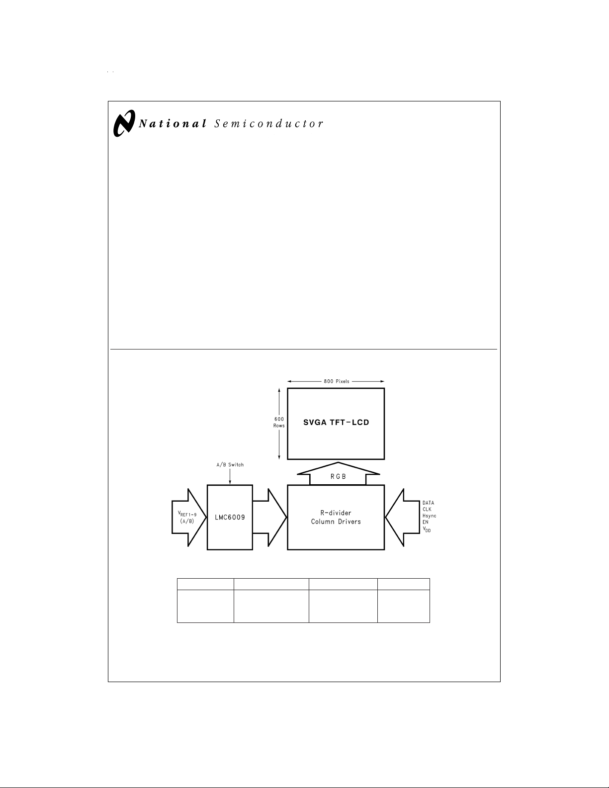
Application in VGA/SVGA TFT-LCD
Features
n Number of inputs 18
n 3.3V and 5V operation
n Supply current 3.5 mA
n Settling time 3 µs
n A/B channel inputs for asymmetrical Gamma
n Number of outputs 9
n Number of control inputs 1
n Built-in thermal shutdown protection
Applications
n VGA/SVGA TFT-LCD drive circuits
n Electronic Notebooks
n Electronic Games
n Personal Communication Devices
n Personal Digital Assistants (PDA)
DS012533-1
Ordering Information
Package Temperature Range Transport Media NSC Drawing
48-pin TSSOP −20˚C–+75˚C MTD48
LMC6009MT
LMC6009MTX Tape and Reel
© 1999 National Semiconductor Corporation DS012533 www.national.com

Absolute Maximum Ratings (Note 1)
If Military/Aerospace specified devices are required,
please contact the National Semiconductor Sales Office/
Distributors for availability and specifications.
ESD Tolerance 1.0 kV
Input Voltage GND–0.3V ≤ V
Supply Voltage (VDD) −0.3 to +6.5 V
Operating Temperature −20˚C to +75˚C
Storage Temperature Range −55˚C to +150˚C
+
+0.3V
V
DD
Maximum Junction Temperature (T
Maximum Power Dissipation (P
) +150˚C
J
) 1.09W
D
Operating Ratings (Note 1)
Supply Voltage 2.7V ≤ V
≤
Frequency DC-50 kHz
DC
Thermal Resistance (θ
DC
Derating 8.70 mW/˚C
)
JA
DD
≤ 5.5V
3V DC Electrical Characteristics
Unless otherwise specified, all limits are guaranteed for T
=
25˚C, and V
J
Symbol Parameter Conditions Min Typ Max Units
V
DD
V
OS
I
B
V
OL
Supply Voltage 2.7 3.0 3.3 V
Offset Voltage RS= 10k 20 mV
Input Bias Current 1500 nA
Output Voltage, Low Amp A8 and A9
=13mA
I
SINK
Amp A1–A7
=13mA
I
V
OH
Output Voltage, High Amp A1 and A2
SINK
I
SOURCE
=13mA
Amp A3–A9
=13mA
I
I
SC
I
DD
∆V
V
IH
V
IL
I
IH
I
IL
A
V
Note 1: See Test Circuit (
Output Short Circuit Current V
Supply Current No Load 3.5 5 mA
Load Regulation VIN= 0.3–3 V
L
A/B Switch Logic Voltage, High Select A 2 V
A/B Switch Logic Voltage, Low Select B 0.8 V
A/B Switch Logic Current, High 1.5 µA
A/B Switch Logic Current, Low 1µA
Voltage Gain 0.985 V/V
Figure 2
)
SOURCE
- 1.65V (Note 1) 80 150 mA
OUT
I
SOURCE
I
SINK
DC
=13mA
= 13 mA +10 mV
=
DD
3.0 V
.
DC
GND +
0.2
GND +
0.6
V
–0.2 V
DD
V
–0.6 V
DD
−10 mV
5V DC Electrical Characteristics
Unless otherwise specified, all limits are guaranteed for T
=
25˚C, and V
J
Symbol Parameter Conditions Min Typ Max Units
V
DD
V
OS
I
B
V
OL
Supply Voltage 4.5 5 5.5 V
Offset Voltage RS= 10k 20 mV
Input Bias Current 1500 nA
Output Voltage, Low Amp A8 and A9
=20mA
I
SINK
Amp A1–A7
=20mA
I
V
OH
Output Voltage, High Amp A1 and A2
SINK
I
SOURCE
=20mA
Amp A3–A9
=20mA
I
I
SC
I
DD
Output Short Circuit Current V
Supply Current No Load 4.5 6 mA
SOURCE
- 1.65V (Note 1) 120 200 mA
OUT
=
.
5V
DD
DC
GND +
0.2
GND +
1.0
V
–0.2 V
DD
V
–1.0 V
DD
V
V
V
V
www.national.com 2

5V DC Electrical Characteristics (Continued)
Unless otherwise specified, all limits are guaranteed for T
=
25˚C, and V
J
Symbol Parameter Conditions Min Typ Max Units
∆V
V
IH
V
IL
I
IH
I
IL
A
V
Load Regulation VIN= 0.5–4.5 V
L
I
SOURCE
I
= 20 mA +10 mV
SINK
=20mA
DC
A/B Switch Logic Voltage, High Select A 2 V
A/B Switch Logic Voltage, Low Select B 0.8 V
A/B Switch Logic Current, High 1.5 µA
A/B Switch Logic Current, Low 1µA
Voltage Gain 0.985 V/V
=
.
5V
DD
DC
−10 mV
AC Electrical Characteristics
Unless otherwise specified, all limits are guaranteed for T
=
25˚C, and V
J
Symbol Parameter Conditions Min Typ Max Units
T
S1
T
S2
Note 2: See test circuits (
Settling Time 1 (Note 2) IDC= 13 mA (Sink/Source) 3 6 µs
Settling Time 2 (Note 2) IDC= 13 mA (Sink/Source) 3 6 µs
Figure 3,Figure 4
and
Figure 5
)
=
.
3V
DD
DC
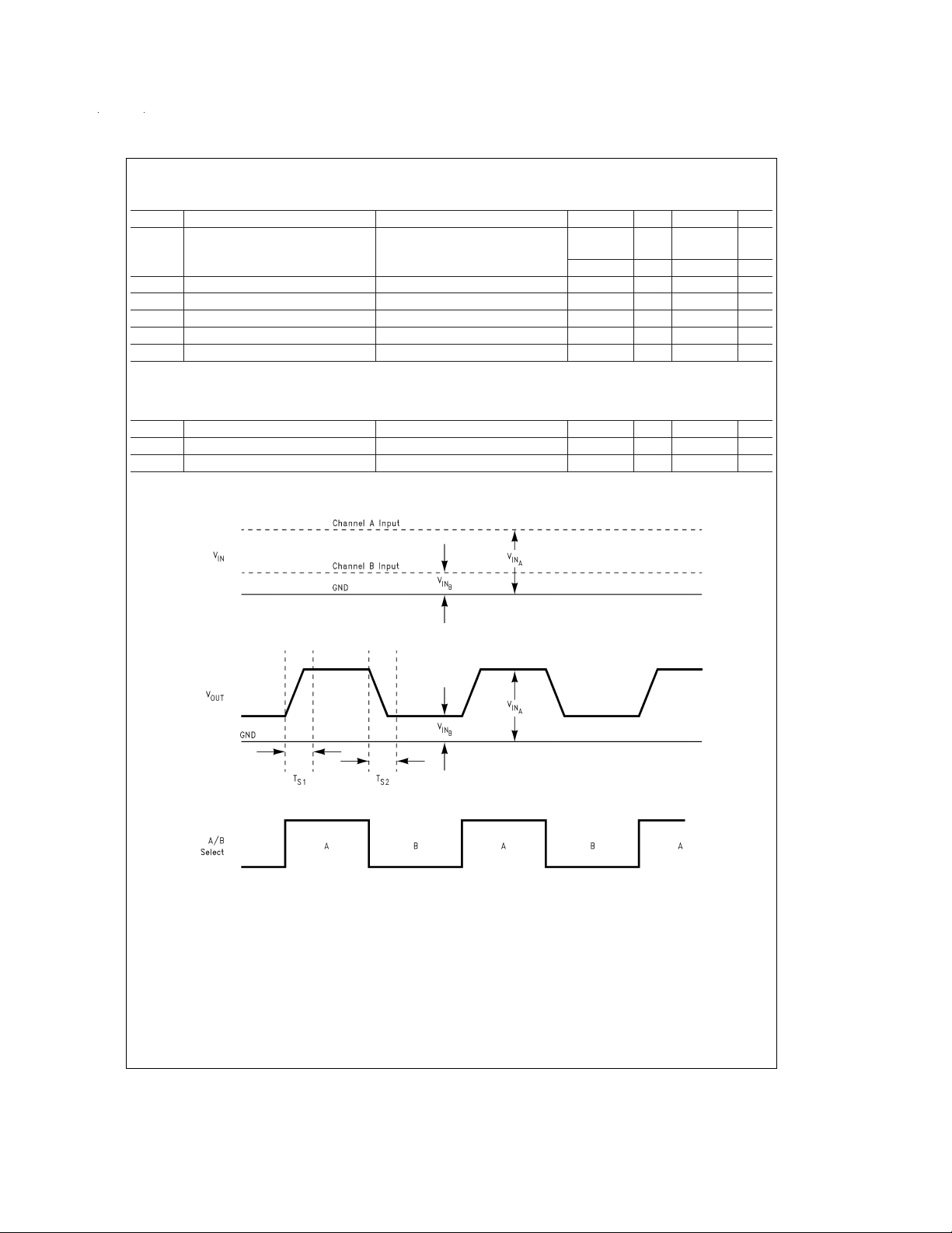
FIGURE 1. Rise and Fall Times at Outputs
DS012533-2
www.national.com3
 Loading...