

LMC6001
Ultra Ultra-Low Input Current Amplifier
General Description
Featuring 100%tested input currents of 25 fA max., low operating power, and ESD protection of 2000V, the LMC6001
achieves a newindustry benchmark for low input current operational amplifiers. By tightly controlling the molding compound, National is able to offer this ultra-low input current in
a lower cost molded package.
To avoid long turn-on settling times common in other low input current opamps, the LMC6001A is tested 3 times in the
first minute of operation. Even units that meet the 25 fA limit
are rejected if they drift.
Because of the ultra-low input current noise of 0.13 fA/
the LMC6001 can provide almost noiseless amplification of
high resistance signal sources. Adding only 1 dB at 100 kΩ,
0.1 dB at 1 MΩ and 0.01 dB or less from 10 MΩ to 2,000 MΩ,
the LMC6001 is an almost noiseless amplifier.
The LMC6001 is ideally suited for electrometer applications
requiring ultra-low input leakage such as sensitive photodetection transimpedance amplifiers and sensor amplifiers.
Since input referred noise is only 22 nV/
√
Hz, the LMC6001
can achieve higher signal to noise ratio than JFET input type
electrometer amplifiers. Other applications of the LMC6001
include long interval integrators, ultra-high input impedance
instrumentation amplifiers, and sensitive electrical-field measurement circuits.
Features
(Max limit, 25˚C unless otherwise noted)
n Input current (100%tested): 25 fA
n Input current over temp.: 2 pA
n Low power: 750 µA
n Low V
√
Hz,
n Low noise: 22 nV/
: 350 µV
OS
Applications
n Electrometer amplifier
n Photodiode preamplifier
n Ion detector
n A.T.E. leakage testing
√
Hz@1 kHz Typ.
LMC6001 Ultra Ultra-Low Input Current Amplifier
March 1995
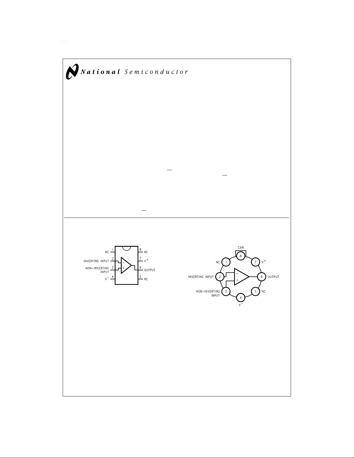
Connection Diagrams
8-Pin DIP
Top View
8-Pin Metal Can
DS011887-1
DS011887-2
Top View
© 1999 National Semiconductor Corporation DS011887 www.national.com
Ordering Information
Package Industrial Temperature Range NSC Package
8-Pin LMC6001AIN, LMC6001BIN, N08E
Molded DIP LMC6001CIN
8-Pin LMC6001AIH, LMC6001BIH H08C
Metal Can
−40˚C to +85˚C Drawing
www.national.com 2
Absolute Maximum Ratings (Note 1)
If Military/Aerospace specified devices are required,
please contact the National Semiconductor Sales Office/
Distributors for availability and specifications.
Differential Input Voltage
Voltage at Input/Output Pin (V
Supply Voltage (V
Output Short Circuit to V
Output Short Circuit to V
+−V−
) −0.3V to +16V
+
−
Lead Temperature
(Soldering, 10 Sec.) 260˚C
Storage Temperature −65˚C to +150˚C
Junction Temperature 150˚C
Current at Input Pin
Current at Output Pin
±
Supply Voltage
+
) + 0.3V, (V−) − 0.3V
(Notes 2, 10)
(Note 2)
±
10 mA
±
30 mA
Current at Power Supply Pin 40 mA
Power Dissipation (Note 9)
ESD Tolerance (Note 9) 2 kV
Operating Ratings (Note 1)
Temperature Range
LMC6001AI, LMC6001BI, LMC6001CI
−40˚C ≤ T
Supply Voltage 4.5V ≤ V
Thermal Resistance (Note 11)
θ
JA
θ
JA
θ
JC
Power Dissipation (Note 8)
≤ +85˚C
J
+
≤ 15.5V
, N Package 100˚C/W
, H Package 145˚C/W
, H Package 45˚C/W
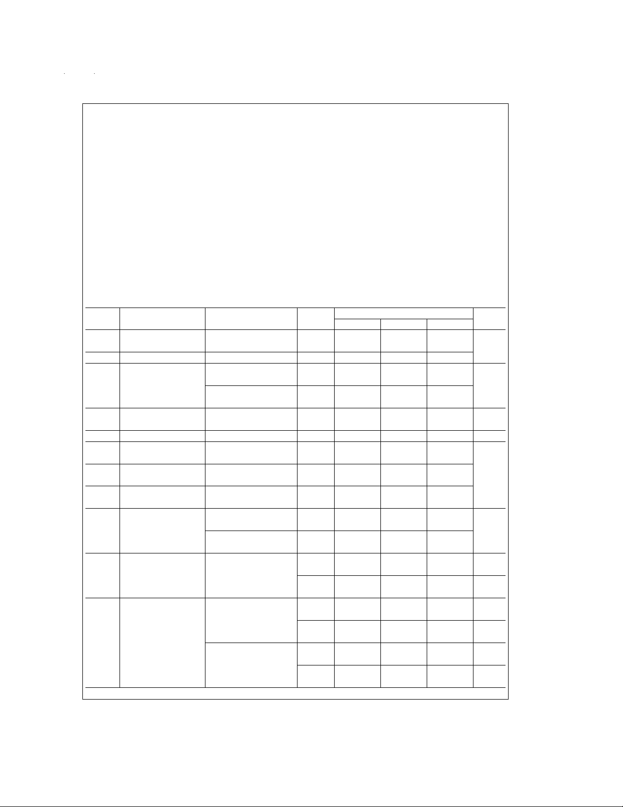
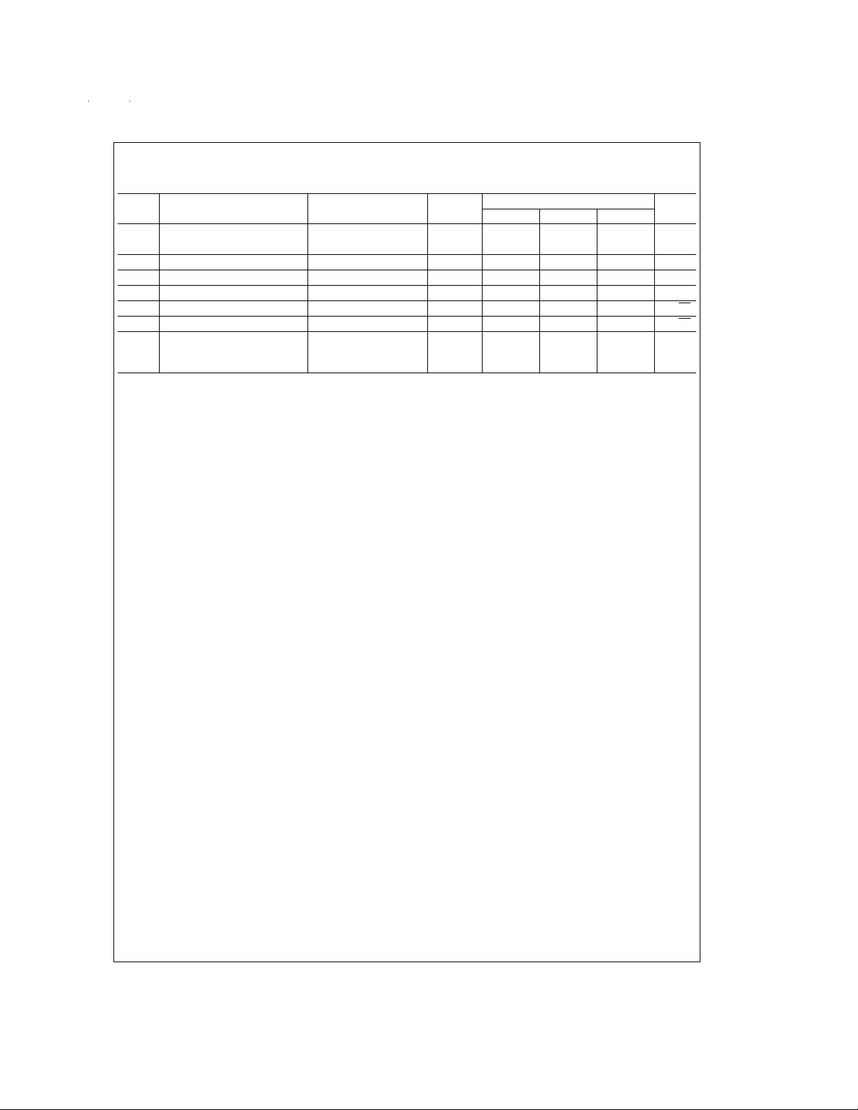
DC Electrical Characteristics
Limits in standard typeface guaranteed for T
otherwise specified, V
+
=
5V, V
−
=
0V, V
Symbol Parameter Conditions
I
B
I
OS
V
OS
TCV
Input Current Either Input, V
Input Offset Current 5 1000 2000 2000
Input Offset Voltage 0.35 1.0 1.0
Input Offset 2.5 10 10 µV/˚C
OS
Voltage Drift
R
IN
Input Resistance
CMRR Common Mode 0V ≤ V
Rejection Ratio V
+PSRR Positive Power Supply 5V ≤ V
Rejection Ratio 70 63 63
−PSRR Negative Power 0V ≥ V
Supply Rejection Ratio 77 71 71
A
V
Large Signal Sourcing, R
Voltage Gain (Note 6) 300 200 200
V
CM
Input Common-Mode V
Voltage For CMRR ≥ 60 dB 000max
V
O
Output Swing V
=
25˚C and limits in boldface type apply at the temperature extremes. Unless
J
=
1.5V, and R
CM
=
S
=
V
S
+
=
Sinking, R
CM
±
5V 2000 4000 4000
±
5V, V
CM
≤ 7.5V 83 75 72 66
CM
10V 72 68 63
+
≤ 15V 83 73 66 66
−
≥ −10V 94 80 74 74
=
2kΩ 1400 400 300 300
L
=
2kΩ 350 180 90 90
L
(Note 6) 100 60 60
+
=
5V and 15V −0.4 −0.1 −0.1 −0.1 V
+
=
5V 4.87 4.80 4.75 4.75 V
=
R
2kΩto 2.5V 4.73 4.67 4.67 min
L
+
=
V
15V 14.63 14.50 14.37 14.37 V
=
R
2kΩto 7.5V 14.34 14.25 14.25 min
L
>
1M.
L
Typical
(Note 4)
=
0V, 10 25 100 1000
LMC6001AI LMC6001BI LMC6001CI
Limits (Note 5) Units
1.0 1.7 2.0
=
0V 0.7 1.35 1.35
1.35 2.0
>
1 Tera Ω
+
V
− 1.9 V+− 2.3 V+− 2.3 V+− 2.3 V
+
V
− 2.5 V+− 2.5 V+− 2.5 min
0.10 0.14 0.20 0.20 V
0.17 0.24 0.24 max
0.26 0.35 0.44 0.44 V
0.45 0.56 0.56 max
fAV
mV
dB
min
V/mV
min
www.national.com3
DC Electrical Characteristics (Continued)
Limits in standard typeface guaranteed for T
otherwise specified, V
+
=
5V, V
−
=
0V, V
Symbol Parameter Conditions
I
O
I
S
Output Current Sourcing, V
Supply Current V
=
25˚C and limits in boldface type apply at the temperature extremes. Unless
J
=
1.5V, and R
CM
+
=
5V, 22 16 13 13
=
V
0V 10 8 8
O
+
Sinking, V
V
O
Sourcing, V
V
O
Sinking, V
V
O
+
+
V
=
5V, 21 16 13 13
=
5V 13 10 10
+
=
15V, 30 28 23 23
=
0V 22 18 18
+
=
=
=
=
15V,
13V (Note 10)
=
5V, V
15V, V
1.5V 450 750 750 750
O
=
7.5V 550 850 850 850
O
>
1M.
L
Typical
(Note 4)
LMC6001AI LMC6001BI LMC6001CI
Limits (Note 5) Units
mA
min
34 28 23 23
22 18 18
900 900 900
µA
max
950 950 950
www.national.com 4
AC Electrical Characteristics
Limits in standard typeface guaranteed for T
otherwise specified, V
+
=
5V, V
−
=
0V, V
Symbol Parameter Conditions Typical Limits (Note 5) Units
SR Slew Rate (Note 7) 1.5 0.8 0.8 0.8 V/µs
GBW Gain-Bandwidth Product 1.3 MHz
φf
G
e
i
n
Phase Margin 50 Deg
m
Gain Margin 17 dB
M
Input-Referred Voltage Noise F=1 kHz 22 nV/√Hz
n
Input-Referred Current Noise F=1 kHz 0.13 fA/√Hz
THD Total Harmonic Distortion F=10 kHz, A
Note 1: Absolute Maximum Ratings indicate limits beyond which damage to the device may occur. Operating Ratings indicate conditions for which the device is intended to be functional but do not guarantee specific performance limits. For guaranteed specifications and test conditions, see the Electrical Characteristics. The
guaranteed specifications apply only for the test conditions listed.
Note 2: Applies to both single supply and split supply operation. Continuous short circuit operation at elevated ambient temperature can result in exceeding the maximum allowed junction temperature of 150˚C. Output currents in excess of
Note 3: The maximum power dissipation is a function of T
=
P
(T
D
Note 4: Typical values represent the most likely parametric norm.
Note 5: All limits are guaranteed by testing or statistical analysis.
Note 6: V
Note 7: V
Note 8: For operating at elevated temperatures the device must be derated based on the thermal resistance θ
Note 9: Human body model, 1.5 kΩ in series with 100 pF.
Note 10: Do not connect the output to V
Note 11: All numbers apply for packages soldered directly into a printed circuit board.
)/θJA.
J(max)−TA
+
=
+
=
=
15V, V
15V. Connected as Voltage Follower with 10V step input. Limit specified is the lower of the positive and negative slew rates.
CM
7.5V and R
connected to 7.5V. For Sourcing tests, 7.5V ≤ VO≤ 11.5V. For Sinking tests, 2.5V ≤ VO≤ 7.5V.
L
+
, when V+is greater than 13V or reliability will be adversely affected.
=
25˚C and limits in boldface type apply at the temperature extremes. Unless
J
CM
=
1.5V and R
>
1M.
L
(Note 4) LM6001AI LM6001BI LM6001CI
0.6 0.6 0.6 min
=
−10,
=
R
L
=
V
O
V
100 kΩ,
8V
PP
±
30 mA over long term may adversely affect reliability.
, θJA, and TA. The maximum allowable power dissipation at any ambient temperature is
J(max)
0.01
JA
with P
=
)/θJA.
(T
D
J−TA
%
www.national.com5
 Loading...