NSC LMC568CN, LMC568CMX, LMC568CM Datasheet

LMC568
Low Power Phase-Locked Loop
General Description
The LMC568 is an amplitude-linear phase-locked loop consisting of a linear VCO, fully balanced phase detectors, and
a carrier detect output. LMCMOS
™
technology is employed
for high performance with low power consumption.
The VCO has a linearized control range of
±
30%to allow demodulation of FM and FSK signals. Carrier detect is indicated when the PLL is locked to an input signal greater than
26 mVrms. LMC568 applications include FM SCA and TV
second audio program decoders, FSK data demodulators,
and voice pagers.
Features
n Demodulates±15%deviation FM/FSK signals
n Carrier Detect Output with hysteresis
n Operation to 500 kHz input frequency
n Low THD—0.5%typ. for
±
10%deviation
n 2V to 9V supply voltage range
n Low supply current drain
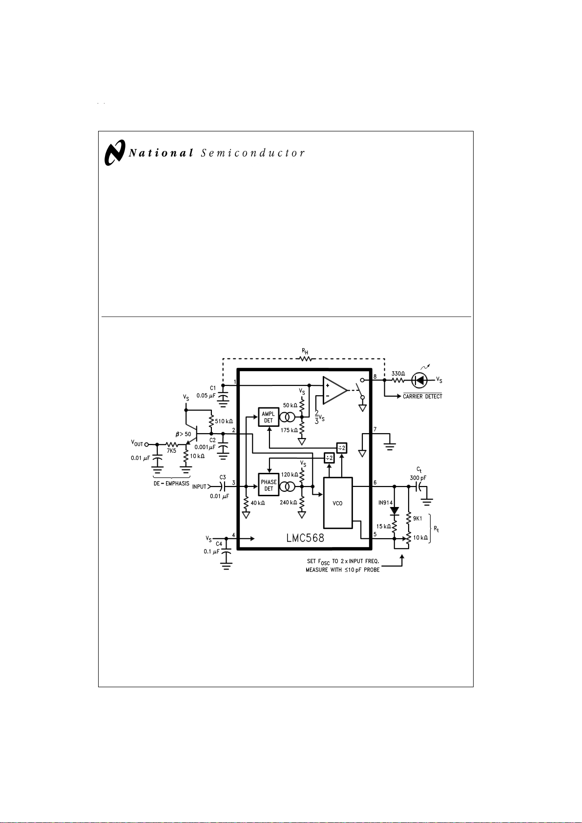
Typical Application (100 kHz input frequency, refer to notes pg. 3)
LMCMOS™is a trademark of NationalSemiconductor Corporation.
DS009135-1
Order Number LMC568CM or LMC568CN
See NS Package Number M08A or N08E
May 1999
LMC568 Low Power Phase-Locked Loop
© 1999 National Semiconductor Corporation DS009135 www.national.com

Absolute Maximum Ratings (Note 1)
If Military/Aerospace specified devices are required,
please contact the National Semiconductor Sales Office/
Distributors for availability and specifications.
Input Voltage, Pin 3 2 V
p–p
Supply Voltage, Pin 4 10V
Output Voltage, Pin 8 13V
Voltage at All Other Pins V
s
to Gnd
Output Current, Pin 8 30 mA
Package Dissipation 500 mW
Operating Temperature Range (T
A
) −25˚C to +125˚C
Storage Temperature Range −55˚C to +150˚C
Soldering Information
Dual-In-Line Package
Soldering (10 seconds) 260˚C
Small Outline Package
Vapor Phase (60 seconds) 215˚C
Infrared (15 seconds) 220˚C
See AN-450 “Surface Mounting Methods and their Effect
on Product Reliability” for other methods of soldering
surface mount devices.
Note 1: “Absolute Maximum Ratings” indicate limits beyond which damage
to the device may occur. Operating Ratings indicate conditions for which the
device is functional, but do not guarantee specific performance limits.
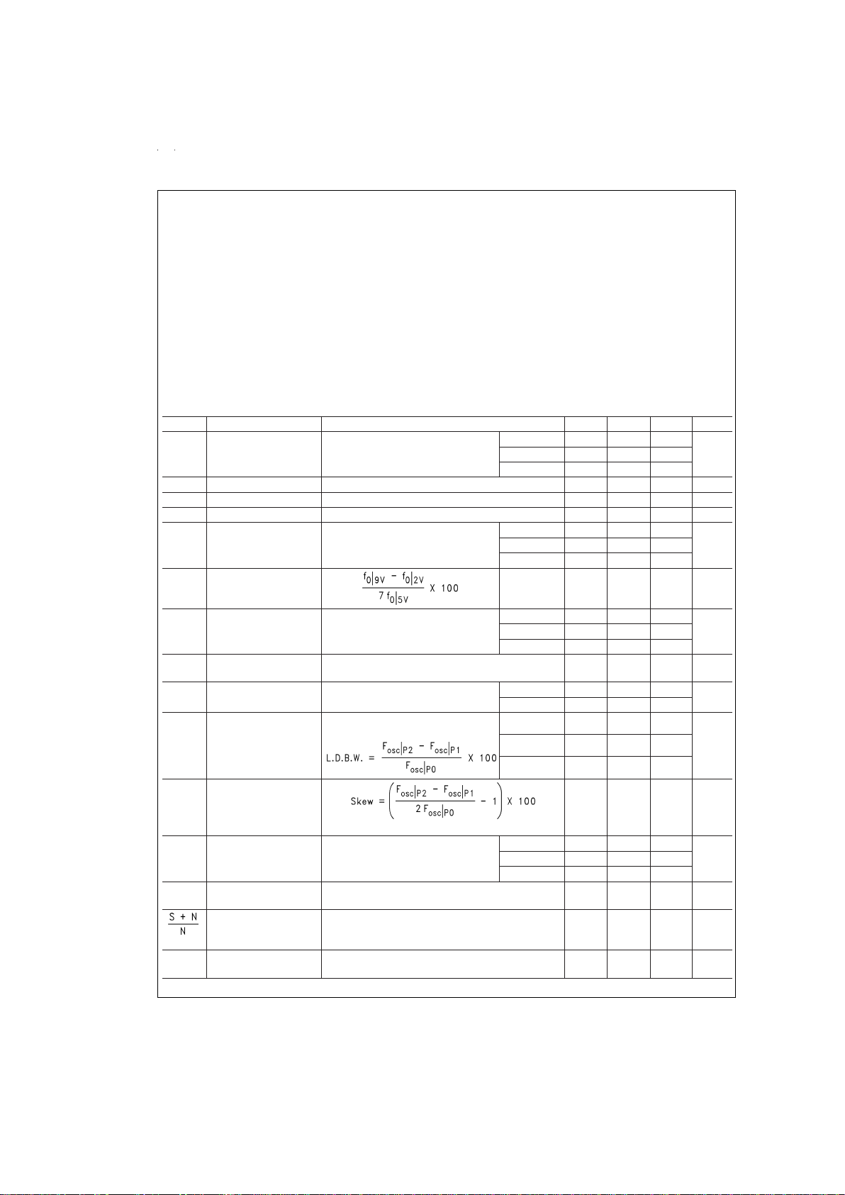
Electrical Characteristics
Test Circuit, T
A
=
25˚C, V
S
=
5V, RtCt
#
2, Sw. 1 Pos. 0; and no input unless otherwise noted.
Symbol Parameter Conditions Min Typ Max Units
I4 Power Supply Current RtCt
#
1, Quiescent or Activated VS= 2V 0.35
mAdcV
S
= 5V 0.75 1.5
V
S
= 9V 1.2 2.4
V3 Input D.C. Bias 0 mVdc
R3 Input Resistance 40 kΩ
I8 Output Leakage 1 100 nAdc
f
0
Center Frequency F
osc
÷
2
RtCt #2, Measure Oscillator
Frequency and Divide by 2
V
S
=2V 98
kHzV
S
= 5V 90 103 115
V
S
= 9V 105
∆f
0
Center Frequency Shift
with Supply
1.0 2.0
%
/V
V
in
Input Threshold Set Input Frequency Equal to f
0
Measured Above, Increase Input
Level until Pin 8 Goes Low.
V
S
= 2V 8 16 25
mVrmsV
S
=5V 15 26 42
V
S
=9V 45
∆V
in
Input Hysteresis Starting at Input Threshold, Decrease Input Level
until Pin 8 Goes High
1.5 mVrms
V8 Output ″Sat″ Voltage Input Level
>
Threshold Choose RL
for Specified I8
I8=2mA 0.06 0.15
Vdc
I8=20mA 0.7
L.D.B.W. Largest Detection
Bandwidth
Measure F
osc
with Sw. 1 in Pos. 0, 1,
and 2;
VS=2V
30
%
V
S
=5V
40 55
V
S
=9V
60
∆BW Bandwidth Skew
1
±
5
%
V
out
Recovered Audio Typical Application Circuit
Input = 100 mVrms, F = 100 kHz
F
mod
= 400 Hz,±10 kHz Dev.
V
S
= 2V 170
mVrmsV
S
= 5V 270
V
S
= 9V 400
THD Total Harmonic
Distortion
Typical Application Circuit as Above, Measure V
out
Distortion.
0.5
%
Signal to Noise Ratio Typical Application Circuit
Remove Modulation, Measure V
n
(S + N)/N = 20 log (V
out/Vn
).
65 dB
f
max
Highest Center Freq. RtCt #3, Measure Oscillator Frequency and Divide by
2
700 kHz
www.national.com 2
 Loading...