

NSC LMC272CMMX, LMC272CMM, LMC272CN, LMC272CMX Datasheet
December 1996
LMC272
CMOS Dual Low Cost Rail to Rail Output Operational
Amplifier
LMC272 CMOS Dual Low Cost Rail to Rail Output Operational Amplifier
General Description
The LMC272 is a CMOS dual operational amplifier with
rail-to-rail output swing and an input common voltage range
that extends below the negative supply. Other performance
characteristics include low voltage operation, low bias current, excellent channel-to-channel isolation, good bandwidth
performance and a competitive price.
These devices are available in MSOP package which is
about half the size of a SO-8 device. This enables the designer to fit the device in extremely small applications.
The LMC272C is a direct replacement for TLC272C with performance which meets or exceeds the TLC272C’s guaranteed limits in the commercial temperature range when operating from a supply of 2.7V to 15V (see Electrical
Characteristics table for details).
These features make this cost effective device ideal for new
designs as well as for upgrading existing designs. Applications include hand-held analytic instruments, transducer amplifiers, sample and hold circuits, etc.
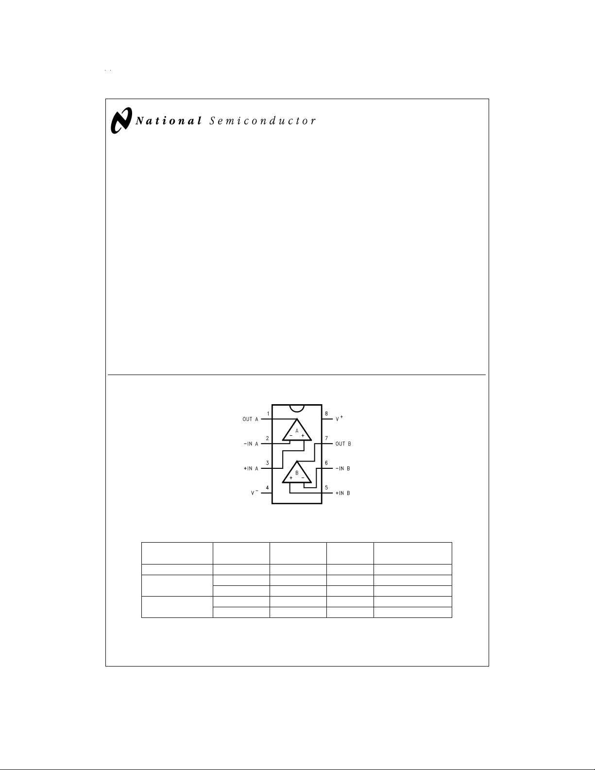
Connection Diagram
Features
=
(Typical unless otherwise noted) V
n Output Swing to within 60 mV of supply rail (10 kΩ load)
n High voltage gain: 90 dB
n Unity gain-bandwidth: 2.0 MHz
n Wide supply voltage: 2.7V to 15V
n Characterized for: 2.7V, 5V, 10V
n Low supply current: 0.975 mA/amplifier
n Input voltage range: −0.3V to 4.2V
S
5V, T
=
25˚C
A
Applications
n Portable instruments
n Upgrade for TLC272C and TS272C
n Photodetector preamplifiers
n D/A converters
n Filters
DS012867-1
Top View
Ordering Information
Package Ordering NSC Drawing Package Supplied as
Information Number Marking
8-pin Molded DIP LMC272CN N08E LMC272CN Rails
8-pin SO-8 LMC272CM M08A LMC272CM Rails
LMC272CMX M08A LMC272CM 2.5k Tape and Reel
MSOP LMC272CMM MUA08A A07 Rails
LMC272CMMX MUA08A A07 3k Tape and Reel
© 1999 National Semiconductor Corporation DS012867 www.national.com
Absolute Maximum Ratings (Note 1)
If Military/Aerospace specified devices are required,
please contact the National Semiconductor Sales Office/
Distributors for availability and specifications.
ESD Tolerance (Note 2) 2 kV
Differential Input Voltage
Voltage at Input/Output Pin (V
Supply Voltage (V
+−V−
): 16V
Current at Input Pin (Note 10)
Current at Output Pin (Note 3)
(Note 7)
Lead Temperature
(soldering, 10 sec.) 260˚C
±
Supply Voltages
+
)+0.3V, (V−)−0.3V
±
5mA
±
30 mA
Storage Temp. Range −65˚C to +150˚C
Junction Temperature (Note 4) 150˚C
Operating Ratings(Note 1)
Supply Voltage 2.5V ≤ V
Junction Temperature Range
LMC272C 0˚C ≤ T
Thermal Resistance (θ
)
JA
N Package, 8-pin Molded DIP 115˚ C/W
M Package, 8-pin Surface Mount 177˚ C/W
MSOP Package 235˚ C/W
≤ 15V
S
≤ +70˚C
J
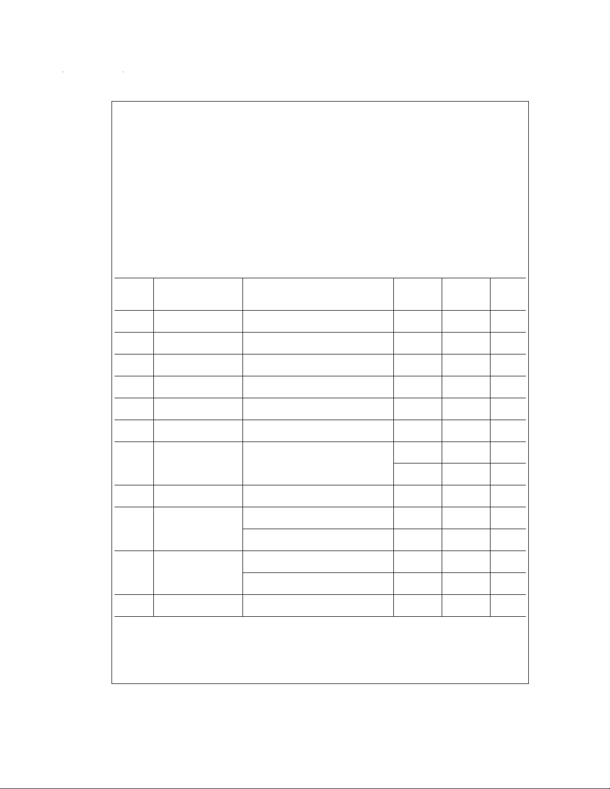
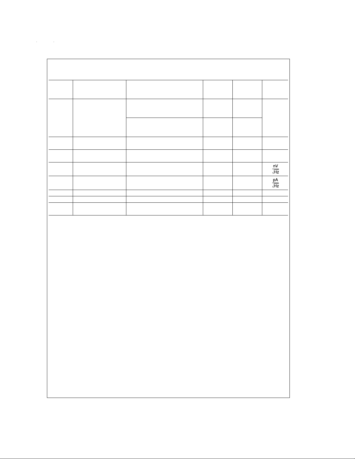
2.7V DC Electrical Characteristics
Unless otherwise specified, all limits guaranteed for T
>
1MΩ.Boldface limits apply at the temperature extremes
J
=
25˚C, V
+
=
2.7V, V
−
=
0V, V
CM
+
=
=
/2, RLto ground, and R
V
V
O
Typ LMC272C
Symbol Parameter Conditions (Note 5) Limit Units
(Note 6)
V
OS
Input Offset Voltage V
O
=
1.4V, R
=
S
50, V
=
=
0V, R
CM
10k 1.40 7 mV
L
9 max
TCV
Temp. Coefficient of T
OS
=
0˚C to 70˚C 3.9 µV/˚C
A
Input Offset Voltage
I
B
Input Bias Current 1 64 pA
max
I
OS
Input Offset Current 0.5 32 pA
max
CMRR Common Mode V
=
−0.2V to 1.2V 77 65 dB
CM
Rejection Ratio 60 min
PSRR Power Supply V+=2.7V to 5V, V
=
1.4V 75 65 dB
O
Rejection Ratio 60 min
V
CM
Input Common-Mode CMRR ≥ 50 dB 1.7 1.5 V
Voltage Range 1.2 min
−0.3 −0.2 V
−0.2 max
A
V
Large Signal Voltage V
=
0.25V to 2.45V, R
O
=
10k 88 dB
L
Gain
V
O
Output Swing R
=
L
10 kΩ,V
=
100 mV 2.64 2.55 V
ID
(Note 11) min
=
V
−100 mV 0 20 mV
ID
(Note 11) 25 max
I
SC
Output Short Circuit Sourcing, V
=
100 mV 3.7 mA
ID
Current (Note 11)
Sinking, V
=
−100 mV 2.5 mA
ID
(Note 11)
I
S
Total Supply Current 1.60 2.5 mA
3.0 max
L
www.national.com 2
2.7V AC Electrical Characteristics
Unless otherwise specified, all limits guaranteed for T
>
1MΩ.Boldface limits apply at the temperature extremes
J
=
25˚C, V
+
=
2.7V, V
−
=
0V, V
CM
+
=
=
/2, RLto ground and R
V
V
O
Typ LMC272C
Symbol Parameter Conditions (Note 5) Limit Units
(Note 6)
=
=
+1, R
SR Slew Rate (Note 8) A
V
VI=1V
10 kΩ,
L
=
20 pF 1.7 V/µs
PP,CL
(Note 12)
GBW Unity Gain Frequency VI=10 mV
=
20 pF 1.9 MHz
PP,CL
(Note 12)
φ
m
Phase Margin VI=10 mVPP,C
=
20 pF 39 Deg
L
(Note 12)
e
n
Input-Referred f=1 kHz, R
=
20Ω
S
27
Voltage Noise
i
n
Input-Referred f=1 kHz
0.0015
Current Noise
f
max
Full Power Bandwidth V
=
S
10V, C
L
=
20 pF, R
=
20 kΩ 120 kHz
L
Amp-to-Amp Isolation (Note 9) 150 dB
THD Total Harmonic A
=
V
+1, V
=
0.7V
IN
PP
0.035
Distortion f=1 kHz
L
%
www.national.com3
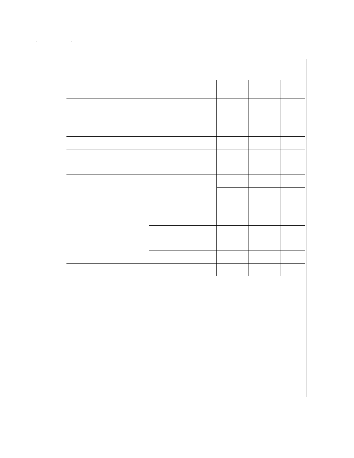
5V DC Electrical Characteristics
Unless otherwise specified, all limits guaranteed for T
1MΩ.Boldface limits apply at the temperature extremes
J
=
25˚C, V
+
=
5V, V
−
=
0V, V
=
CM
+
=
/2, RLto ground and R
V
V
O
Typ LMC272C
Symbol Parameter Conditions (Note 5) Limit Units
(Note 6)
V
OS
TCV
Input Offset Voltage V
OS
Temp. Coefficient of T
=
1.4V, R
O
=
R
10k, V
L
=
0˚C to 70˚C 3.3 µV/˚C
A
=
50, 1.75 7 mV
S
=
0V 9 max
CM
Input Offset Voltage
I
B
I
OS
CMRR Common Mode V
Input Bias Current 1 64 pA
Input Offset Current 0.5 32 pA
=
−0.2V to 3.5V 77 65 dB
CM
Rejection Ratio 60 min
PSRR Power Supply V+=5V to 10V, V
=
1.4V 88 65 dB
O
Rejection Ratio 60 min
V
CM
Input Common-Mode CMRR ≥ 50 dB 4.2 4 V
Voltage Range 3.5 min
−0.3 −0.2 V
−0.2 max
A
V
Large Signal Voltage V
=
0.25V to 2V, R
O
=
10k 90 80 dB
L
Gain 72 min
V
O
Output Swing R
=
L
10 kΩ,V
=
100 mV 4.94 4.85 V
ID
(Note 11) 4.75 min
=
V
−100 mV 0 20 mV
ID
(Note 11) 25 max
I
SC
Output Short Circuit Sourcing, V
=
100 mV 16 mA
ID
Current (Note 11)
Sinking, V
=
−100 mV 16 mA
ID
(Note 11)
I
S
1.95 3.2 mA
3.6 max
L
max
max
>
www.national.com 4
5V AC Electrical Characteristics
Unless otherwise specified, all limits guaranteed for T
1MΩ.Boldface limits apply at the temperature extremes
J
=
25˚C, V
+
=
5V, V
−
=
0V, V
=
CM
+
=
/2, RLto ground and R
V
V
O
Typ LMC272C
Symbol Parameter Conditions (Note 5) Limit Units
(Note 6)
=
=
+1, R
SR Slew Rate (Note 8) A
V
VI=1V
10 kΩ, V/µs
L
=
20 pF 2.5
PP,CL
(Note 12)
=
+1, R
=
10 kΩ,
L
=
20 pF 2.5
PP,CL
A
V
VI=2.5 V
(Note 12)
GBW Unity Gain Frequency VI=10 mV, C
=
20 pF 2.0 MHz
L
(Note 12)
φ
m
Phase Margin VI=10 mV, C
=
20 pF 43 Deg
L
(Note 12)
e
n
Input-Referred f=1 kHz, R
=
20Ω
S
25
Voltage Noise
i
n
Input-Referred f=1 kHz
0.0015
Current Noise
f
max
Full Power Bandwidth V
=
S
10V, C
L
=
20 pF, R
=
20 kΩ 120 kHz
L
Amp-to-Amp Isolation (Note 9) 150 dB
THD Total Harmonic A
=
V
+1, V
=
2.5 V
IN
PP
0.015
Distortion f=1 kHz
>
L
%
www.national.com5
 Loading...