

TL/H/12541
LMC2626 CMOS LDOR/Buffer Chip for Row Inversion Flat Panel Display Systems
PRELIMINARY
November 1995
LMC2626
CMOS LDOR/Buffer Chip for Row
Inversion Flat Panel Display Systems
General Description
The LMC2626 integrated circuit is specifically developed for
a row inversion TFT FPD system architecture. It is designed
only to be used in conjunction with National’s LM2625
switching regulator chip.
Built on National’s advanced CMOS CS80 process, this chip
generates a high-power, precision square-wave from a digital sync signal. The chip also contains thermal shutdown
circuitry, system shutdown circuitry, and a low drop-out voltage regulator to generate a 4.2 volt supply from an externally applied reference voltage of 1.227V.
Features
Y
Used in conjunction with LM2625 chip
Y
High output current buffer
Y
Low buffer on resistance
Y
System shutdown control
Y
LDO voltage regulator
Y
LDOR dropout 0.3V maximum at 150 mA
Y
Thermal shutdown/short circuit protection
Y
External reference required for LDOR
Y
V
REF
pin converts to a digital pin to shutdown LM2625
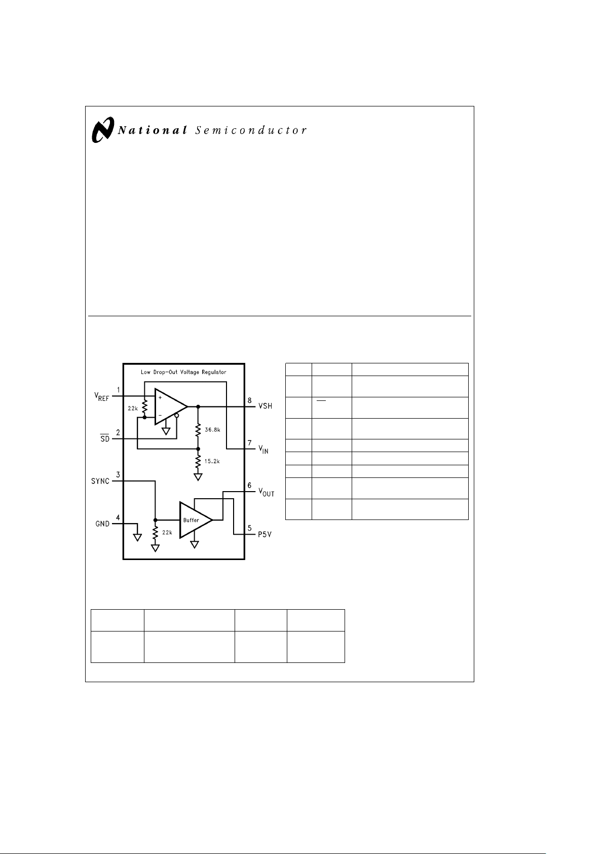
Connection Diagram
8-Pin SO
TL/H/12541– 1
Top View
Pin Description
PinÝPin Name Description
1V
REF
1.218V to 1.242V Ext. Reference
from LM2625 (see Note 8)
2SD System Shutdown input pin for
LMC2626 and LMC2625
3 SYNC Digital input square wave from FPD
controller
4 GND Ground
5 P5V Precision Regulateda5V Supply
6V
OUT
Power Buffer Output
7VINFPD System Supply (a4.5V to
a
5.5V)
8VSHLow Drop-Out Voltage Regulator
Output
Ordering Information
Package
Temperature Range NSC Transport
b
40§Ctoa85§C Drawing Media
8-Pin SO LMC2626IM M08A Rail
Tape and
Reel
C
1996 National Semiconductor Corporation RRD-B30M26/Printed in U. S. A.
Absolute Maximum Ratings (Note 1)
ESD Tolerance 2 kV HBM, 200V MM (Note 4)
Sync Input Voltage P5V
Supply Voltage (V
IN
, P5V) 6.3V
Continuous Total Power Dissipation (Note 1)
Lead Temperature (less than 10 sec) 260§C
Storage Temperature Range
b
65§Ctoa150§C
Junction Temperature 150§C
Operating Ratings (Note 1)
V
IN
Supply Voltage 4.5VsV
IN
s
5.5V
P5V Supply Voltage (Note 5) 4.8VsP5Vs5.2V
Junction Temperature Range
b
25§Ctoa125§C
Ambient Temperature Range
b
40§Ctoa85§C
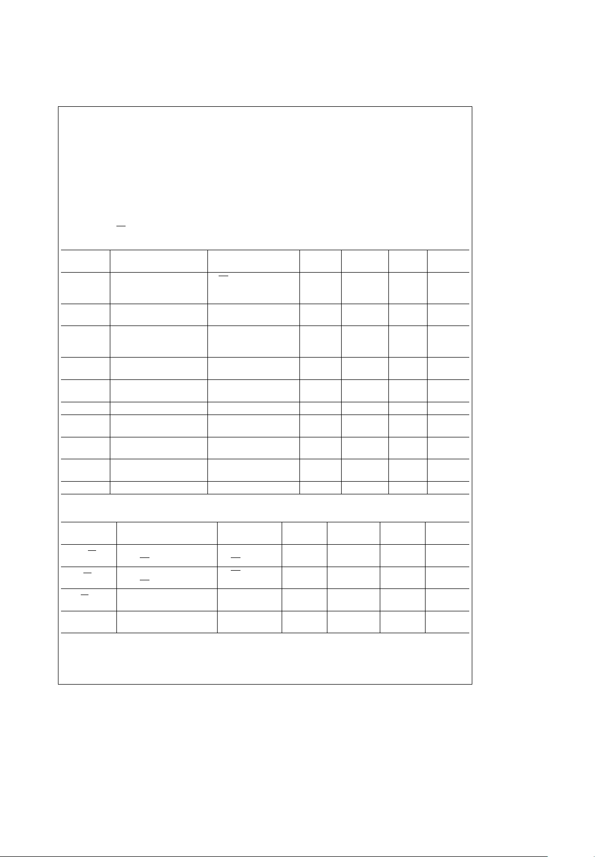
DC Electrical Characteristics
Unless otherwise specified, all limits guaranteed forb20§CsT
A
s
a
85§C, P5Ve5V and 4.5VsV
IN
s
5.5V, V
REF
e
1.227V
SYNC(OPEN), SD
(OPEN)kP5VeV
IN
e
5V
VSH LDO Voltage Regulator (Notes 7, 10, 11)
Symbol Parameter Conditions Min
Typ
Max Units
(Note 9)
V
O(VREF)
V
REF
Voltage Level SDe0V
in Shutdown I
VREF
eb
1 mA 4.00 4.76 V
V
IN
e
5V
I
VREF
DC Current from
b
40.0
b
13.3
b
5 mA
V
REF
Pin
V
SH
Output Voltage on 4.5VsV
IN
s
5.5V
V
SH
Pin (see Note 2) 20 mAsILs150 mA 4.10 4.20 4.30 V
1.218
s
V
REF
s
1.242
DV
SH
Variation of VSHover 4.5VsV
IN
s
5.5V
4 126 mV
Temperature 20 mA
sILs
150 mA
V
DO
LDOR Voltage Dropout ILe150 mA
0.17 0.30 V
(VIN–VSH)
I
S(VIN)
VINSupply Current 230 394 500 mA
Load Regulation of LDO 4.5VsV
IN
s
5.5V
0.002 0.015 %/mA
Voltage Regulation 20 mA
sILs
150 mA
Line Regulation of LDOR 4.5VsV
IN
s
5.5V
0.24 0.95 %/V
20 mA
sILs
150 mA
T
SD
Thermal Shutdown (see Note 8)
160
§
C
Threshold
I
OUT
Output Load Current (see Note 2) 300 mA
Shutdown Control (Note 8)
Symbol Parameter Conditions Min
Typ
Max Units
(Note 9)
I
IL(SD)
Low Level Input Current V
IN
e
5V
b
300
b
217
b
150 mA
for SD
Pin SDe0V
I
IH(SD)
High Level Input Current SDe5V
310 1000 nA
for SD
Pin
I
s(SD)
VINSupply Current
180 285 400 mA
in Shutdown Mode
C
in(SYNC)
Input Capacitance SYNCe5V
20 pF
at SYNC Pin (Note 6) T
A
e
27§C
2
 Loading...