

August 1999
LMC2001
High Precision, 6MHz Rail-To-Rail Output Operational
Amplifier
LMC2001 High Precision, 6MHz Rail-To-Rail Output Operational Amplifier
General Description
The LMC2001 is a new precision amplifier that offers unprecedented accuracy and stability at an affordable price
and is offered in miniature (SOT23-5) package. This device
utilizes patented techniques to measure and continually correct the input offset error voltage. The result is an amplifier
which is ultra stableovertime,andtemperature.It has excellent CMRR and PSRR ratings, and does not exhibit the familiar 1/f voltage and current noise increase that plagues traditional amplifiers. The combination of the LMC2001
characteristics makes it a good choice for transducer amplifiers, high gain configurations, ADC buffer amplifiers, DAC
I-V conversion, and any other 5V application requiring precision and/or stability.
Other useful benefits of the LMC2001 are rail-to-rail output,
low supply current of 750µA, and wide gain-bandwidth
product of 6MHz. The LMC2001 comes in 5 pin SOT23 and
8 pin SOIC. These extremely versatile features found in the
LMC2001 provide high performance and ease of use.
Connection Diagrams
8-Pin SO
DS100058-1
Top View
Features
(Vs=5V,RL= 10K to V+/2, Typ. Unless Noted)
n Low Guaranteed V
n e
With No 1/f 85nV/
n
n High CMRR 120dB
n High PSRR 120dB
n High A
VOL
n Wide Gain-Bandwidth Product 6MHz
n High Slew Rate 5V/µs
n Low Supply Current 750µA
n Rail-To-Rail Output 30mV from either rail
n No External Capacitors Required
os
40µV
137dB
Applications
n Precision Instrumentation Amplifiers
n Thermocouple Amplifiers
n Strain Gauge Bridge Amplifier
5-Pin SOT23
DS100058-2
Top View
Ordering Information
Package Temperature Range Package
Commercial
0˚C to +70˚C
8-pin Small Outline LMC2001AIM LMC2001AIM Rails M08A
5-pin SOT23-5 LMC2001ACM5 A09A 1k Units Tape
LMC2001ACM5X 3k Units Tape
© 1999 National Semiconductor Corporation DS100058 www.national.com
Industrial
−40˚C to +85˚C
LMC2001AIMX 2.5k Units Tape
Marking
Transport
Media
and Reel
and Reel
and Reel
NSC
Drawing
MA05B
Absolute Maximum Ratings (Note 1)
If Military/Aerospace specified devices are required,
please contact the National Semiconductor Sales Office/
Distributors for availability and specifications.
ESD Tolerance (Note 2)
Human Body Model 2500V
Machine Model 150V
Differential Input Voltage
Supply Voltage (V
+-V-
) 5.6V
Current At Input Pin 30mA
Current At Output Pin 30mA
Current At Power Supply Pin
(Note 3)
±
Supply Voltage
50mA
Storage Temperature Range -65˚C to 150˚C
Junction Temperature (T
(Note 4)
)
J
150˚C
Operating Ratings (Note 1)
Supply voltage 4.75V to 5.25V
Temperature Range
LMC2001AI -40˚C ≤ T
LMC2001AC 0˚C ≤ T
Thermal resistance ( θ
)
JA
M Package, 8-pin Surface Mount 180˚C /W
M5 Package, SOT23-5 274˚C /W
≤ 85˚C
J
≤ 70˚C
J
Lead Temperature (soldering, 10
260˚C
sec)
DC Electrical Characteristics
Unless otherwise specified, all limits guaranteed for TJ= 25˚C, V+= 5V, V-= 0V, VCM= 2.5V, VO= 2.5V and R
Boldface limits apply at the temperature extremes.
Symbol Parameter Conditions
V
OS
Input Offset Voltage (Note 11) 0.5 40
Offset Calibration Time 5 30 ms
TCV
Input Offset Voltage (Note 12) 0.015 µV/˚C
OS
Long-Term Offset Drift (Note 8) 0.006 µV/month
Lifetime V
I
IN
I
OS
R
IND
Input Current (Note 9) -3 pA
Input Offset Current 6 pA
Input Differential Resistance 9 MΩ
CMRR Common Mode Rejection
Ratio
PSRR Power Supply
drift (Note 8) 2.5 5 µV Max
OS
0V ≤ V
CM
0.1V ≤ V
CM
4.75V ≤ V
Rejection Ratio
A
VOL
V
O
I
O
Large Signal Voltage Gain
(Note 7)
Output Swing R
Output Current Sourcing, VO=0V
RL= 10kΩ 137 105
=2kΩ 128 95
R
L
=
10kΩ to 2.5V
L
=
(diff)
V
IN
=
R
2kΩ to 2.5V
L
=
(diff)
V
IN
(diff) =±0.5V
V
IN
Sinking, V
(diff) =±0.5V
V
I
S
Supply Current 0.75 1.0
IN
Typ
(Note 5)
≤ 3.5V 120 100 dB
≤ 3.5V 110 90 dB
+
≤ 5.25V 120 95
4.975 4.955
±
0.5V
0.030 0.060
4.936 V
±
0.5V
0.075 V
5.9 4.1
O
=5V
14.5 4.5
Limit(Note 6)
60
90
100
90
4.955
0.060
1.5
1.5
1.2
>
1MΩ.
L
Units
µV
max
min
min
dB
min
dB
min
V
min
V
max
mA
min
mA
min
mA
max
www.national.com 2
AC Electrical Characteristics
TJ= 25˚C, V+= 5V, V-= 0V, VCM= 2.5V, VO= 2.5V, and R
Symbol Parameter Conditions
SR Slew Rate A
= +1, Vin=3.5Vpp 5 V/µs
V
GBW Gain-Bandwidth Product 6 MHz
θ
G
e
n
Phase Margin 75 Deg
m
Gain Margin 12 dB
m
Input-Referred Voltage Noise f = 0.1Hz 85 nV/
enp-p Input-Referred Voltage Noise RS= 100Ω, DC to 10Hz 1.6 µVpp
i
n
Input-Referred Current Noise f = 0.1Hz 180 fA/
>
1MΩ.
L
Typ
(Note 5)
Units
THD Total Harmonic Distortion f = 1kHz, Av = -2
= 10kΩ,VO= 4.5Vpp
R
L
0.02
trec Input Overload Recovery Time 50 ms
T
S
Output Settling time (Note 10) A
(Note 10)A
Note 1: Absolute Maximum Ratings indicate limits beyond which damage to the device may occur. Operating Ratings indicate conditions for which the device is intended to be functional, but specific performance is not guaranteed. For guaranteed specifications and test conditions, see the Electrical Characteristics.
Note 2: Human body model, 1.5kΩ in series with 100pF. Machine model, 200Ω in series with 100pF.
Note 3: Output currents in excess of
Note 4: The maximum power dissipation is a function of T
-TA)/θJA. All numbers apply for packages soldered directly onto a PC board.
Note 5: Typical values represent the most likely parametric norm.
Note 6: All limits are guaranteed by testing or statistical analysis, unless otherwise noted.
+
Note 7: V
=5V,VCM= 2.5V, and RLconnected to 2.5V. For Sourcing tests, 2.5V ≤ VO≤ 4.8V. For Sinking tests, 0.2V ≤ VO≤ 2.5V.
Note 8: Guaranteed Vos Drift is based on 280 devices operated for 1000 hrs at 150˚C (equivalent to 30 years 55ºC).
Note 9: Guaranteed by design only.
Note 10: Settling times shown correspond to the worse case (positive or negative step) and does not include slew time. See the Application Note section for test
schematic.
Note 11: The limits are set by the accuracy of high speed automatic test equipment. For the typical V
Note 12: Precision bench measurement of more than 300 units. More than 65%of units had less than 15nV /˚C V
±
30mA over long term may adversely affect reliability.
=
+1, 1V step 1
V
=
−1, 1V step 1
V
, θJA, and TA. The maximum allowable power dissipation at any ambient temperature is PD=(T
J(max)
%
%
0.1
%
0.01
%
%
0.1
%
0.01
distribution, see the curve on page 4.
OS
OS
250 ns
400
3200
80
860
1400
J(max)
drift.
%
www.national.com3
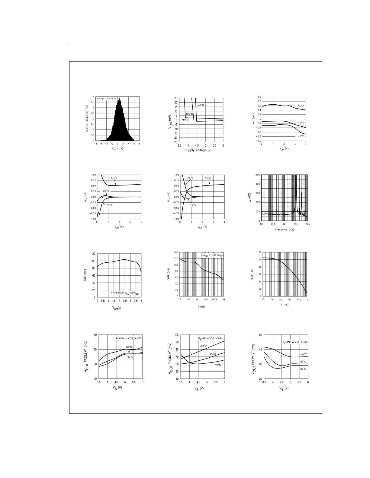
Typical Performance Characteristics
=
T
A
25C, V
=
5V unless otherwise specified.
S
Distribution
V
OS
VOSvs V
S
VOSvs V
CM
+IINvs V
CMR vs V
+
V
vs V
OUT
CM
CM
S
DS100058-63
DS100058-68
DS100058-92
DS100058-91
−IINvs V
CM
DS100058-A4
CMR vs Frequency
DS100058-65
+
V
vs V
OUT
S
DS100058-97
eNvs Frequency
PSR vs Frequency
DS100058-66
−
V
vs V
OUT
S
DS100058-A0
DS100058-89
www.national.com 4
DS100058-88
DS100058-99
 Loading...