

NSC LM98501CCVBH Datasheet
LM98501
10-Bit, 27 MSPS Camera Signal Processor
General Description
The LM98501 is a CCD signal processor for electronic cameras. The processor provides a common interface to a number of different image sensors including CCD, CMOS, and
CIS. Correlated double sampling reduces kTC noise from
the image signal. A fast, temperature stable, 8-bit digitally
programmable gain amplifier enables pixel-rate
white-balancing. An auxiliary input is provided, allowing for
the selection of anexternalsignal, useful for electronic titling
and video overlay. The 10-bit A/D converter preserves the
image quality with excellent noise performance. The
LM98501 also includes the supporting functions of digital
black level clamp and power down, ideally suited for portable
video applications. This low-power processor is a natural
choice for the most demanding imaging systems.
Applications
n Digital still camera
n Digital video camcorder
n Video conferencing
n Security camera
n Plain paper copier
n Flatbed or handheld color scanner
n Video processing for x-ray or infrared
n Barcode scanner
Features
n +3V single power supply
n Low power CMOS design
n 4-wire serial interface
n 2.5V data output voltage swing
n No missing codes
n AUX input with input clamp and programmable gain
n Four color gain and offset registers
n Digital black level clamp
n Small 48-lead LQFP package
Key Specifications
j
Maximum Input Level 1.0V peak-peak
j
CDS Sampling Rate 27 MSPS
j
PGA Gain Steps 256 Steps
j
PGA Gain Range 0.0 dB-32.0 dB
j
ADC Resolution 10-Bit
j
ADC Sampling Rate 27 MSPS
j
*Signal-to-Noise Ratio 60 dB 0 dB Gain, 1.0V Input
j
Power Dissipation
AV+ = DV+ = DV+ I/O = 3.0V 195 mW (typical)
j
Operating Temperature 0˚C to 70˚C
*
20 log10(VIN/RMS Output Noise)
LM98501 10-Bit, 27 MSPS Camera Signal Processor
February 2000
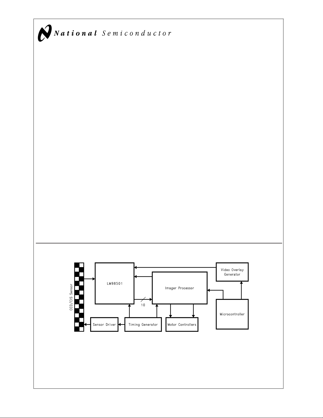
Typical Digital Camera Block Diagram
DS101292-1
© 2000 National Semiconductor Corporation DS101292 www.national.com
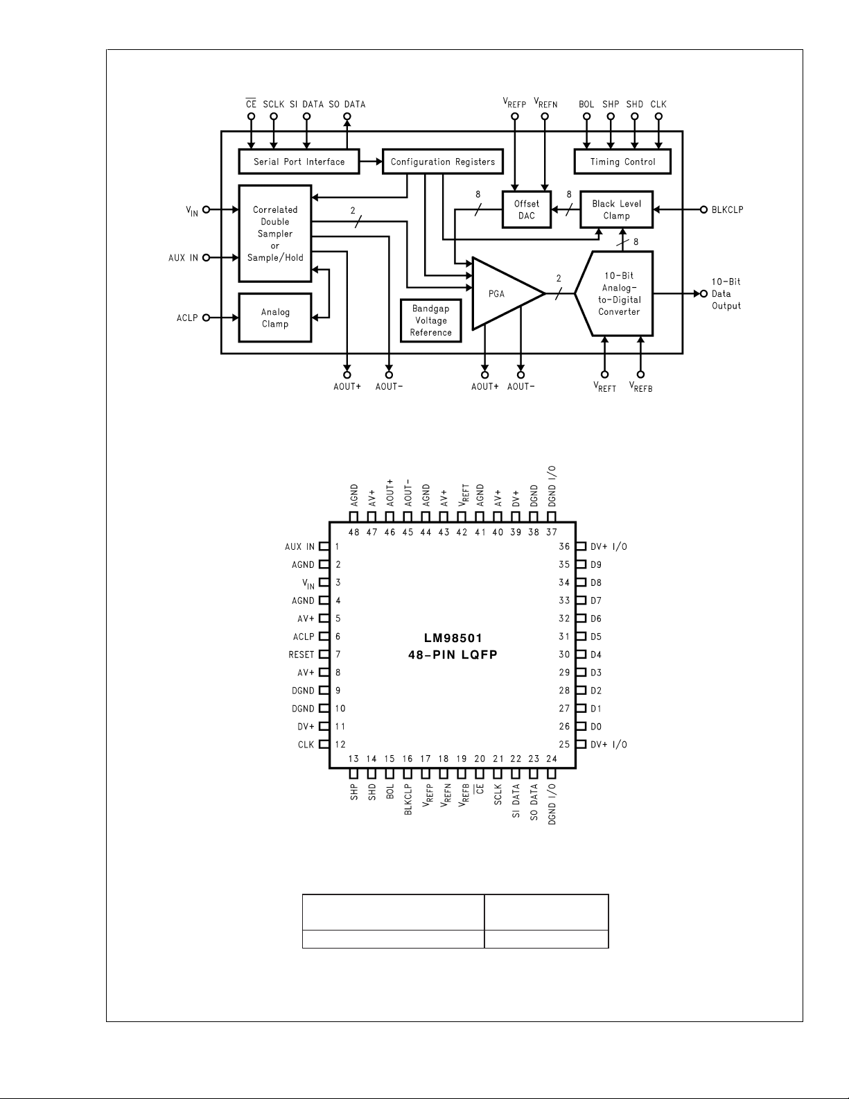
Overall Chip Block Diagram
LM98501
LM98501 Chip Pin Out
DS101292-2
FIGURE 1. Chip Block Diagram
FIGURE 2. Pin Out Diagram
Ordering Information
Commercial
(0˚C ≤ T
LM98501CCVBH LQFP
www.national.com 2
≤ +70˚C)
A
DS101292-3
NS Package
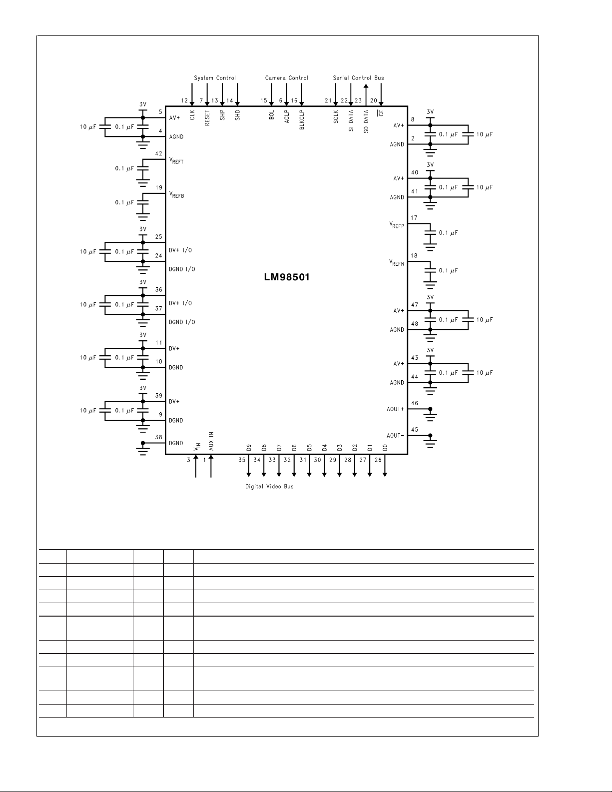
Typical Application Circuit
LM98501
DS101292-4
FIGURE 3. Typical Application Circuit Diagram
Pin Descriptions
Pin Name I/O Typ Description
1 AUX IN I A Auxiliary analog input.
2 AGND P Analog ground return.
3V
4 AGND P Analog ground return.
5 AV+ P +3V power supply for the analog circuits. Bypass each supply pin with 0.1 µF and
6 ACLP I D Analog clamp switch. Float pin when function not being used.
7 RESET I D Active-high master reset. Float pin when function not being used.
8 AV+ P +3V power supply for the analog circuits. Bypass each supply pin with 0.1 µF and
9 DGND P Digital ground return.
10 DGND P Digital ground return.
IN
I A Analog input. AC-couple input signal through a 0.1 µF capacitor
10 µF capacitors in parallel.
10 µF capacitors in parallel.
www.national.com3
Pin Descriptions (Continued)
Pin Name I/O Typ Description
LM98501
11 DV+ P +3V power supply for the digital circuits. Bypass each supply pin with 0.1 µF and
10 µF capacitors in parallel.
12 CLK I D 27 MHz clock input.
13 SHP I D Correlated double sampler reset voltage clamp override. Programmable active-high or
active-low through serial interface. Connect to +3V digital supply when function not
being used (register values in default condition).
14 SHD I D Correlated double sampler video signal voltage sample override. Programmable
active-high or active-low through serial interface. Connect to +3V digital supply when
function not being used (register values in default condition).
15 BOL I D Active-high beginning of line switch input. Hold high during entire line of effective
pixels. Hold low during blanking period.
16 BLKCLP I D Active-high black level clamp switch input. Pulse high during black pixels to eliminate
black pixel offset from video signal.
17 V
18 V
19 V
REFP
REFN
REFB
20 CE
21 SCLK I D Serial interface clock used to decode the serial input data.
22 SI DATA I D Serial interface input port.
23 SO DATA O D Serial interface output port.
24 DGND I/O P Digital output driver ground return.
25 DV+ I/O P +3V power supply for the digital output driver circuits. Bypass each supply pin with
26 D0 O D Digital output. Bit 0 of 9 (LSB) of the digital video output bus.
27 D1 O D Digital output. Bit 1 of 9 of the digital video output bus.
28 D2 O D Digital output. Bit 2 of 9 of the digital video output bus.
29 D3 O D Digital output. Bit 3 of 9 of the digital video output bus.
30 D4 O D Digital output. Bit 4 of 9 of the digital video output bus.
31 D5 O D Digital output. Bit 5 of 9 of the digital video output bus.
32 D6 O D Digital output. Bit 6 of 9 of the digital video output bus.
33 D7 O D Digital output. Bit 7 of 9 of the digital video output bus.
34 D8 O D Digital output. Bit 8 of 9 of the digital video output bus.
35 D9 O D Digital output. Bit 9 of 9 (MSB) of the digital video output bus.
36 DV+ I/O P +3V power supply for the digital output driver circuits. Bypass each supply pin with
37 DGND I/O P Digital output driver ground return.
38 DGND P Digital ground return.
39 DV+ P +3V power supply for the digital circuits. Bypass each supply pin with 0.1 µF and 10
40 AV+ P +3V power supply for the analog circuits. Bypass each supply pin with 0.1 µF and 10
41 AGND P Analog ground return.
42 V
REFT
43 AV+ P +3V power supply for the analog circuits. Bypass each supply pin with 0.1 µF and 10
44 AGND P Analog ground return.
45 AOUT− O A Negative differential analog output from correlated double sampler or PGA (selectable
IO A Top of DAC reference ladder. Normally bypassed with a 0.1 µF capacitor. An external
DAC reference voltage may be applied to this pin.
IO A Bottom of DAC reference ladder. Normally bypassed with a 0.1 µF capacitor. An
external DAC reference voltage may be applied to this pin.
IO A Bottom of ADC reference ladder. Normally bypassed with a 0.1 µF capacitor. An
external ADC reference voltage may be applied to this pin.
I D Active-low chip enable for the serial interface.
0.1 µF and 10 µF capacitors in parallel.
0.1 µF and 10 µF capacitors in parallel.
µF capacitors in parallel.
µF capacitors in parallel.
IO A Top of ADC reference ladder. Normally bypassed with a 0.1 µF capacitor. An external
ADC reference voltage may be applied to this pin.
µF capacitors in parallel.
through the serial interface).
www.national.com 4
Pin Descriptions (Continued)
Pin Name I/O Typ Description
46 AOUT+ O A Positive differential analog output from correlated double sampler or PGA (selectable
through the serial interface).
47 AV+ P +3V power supply for the analog circuits. Bypass each supply pin with 0.1 µF and 10
µF capacitors in parallel.
48 AGND P Analog ground return.
Legend: (I=Input), (O=Output), (IO=Bi-directional), (P=Power), (D=Digital), (A=Analog).
LM98501
www.national.com5
Absolute Maximum Ratings (Notes 1, 2)
If Military/Aerospace specified devices are required,
LM98501
please contact the National Semiconductor Sales Office/
Distributors for availability and specifications.
Any Positive Supply Voltage 4.2V
Voltage on Any Input or Output Pin −0.3V to +4.2V
Input Current at Any Pin (Note 3)
Package Input Current (Note 3)
=
Package Dissipation at T
(Note 4)
25˚C
A
±
35 mA
±
50 mA
ESD Susceptibility (Note 5)
Human Body Model 2000V
Machine Model 200V
Soldering Temperature Infrared,
10 seconds (Note 6) 260˚C
DC and Logic Level Specifications
The following specifications apply for DV+=AV+=DV + I/O=+3.0V, C
noted. Boldface limits apply for T
Symbol Parameter Conditions
DIGITAL INPUT CHARACTERISTICS
V
IH
V
IL
I
IH
I
IL
Logical “1” Input Voltage 2.0 V
Logical “0” Input Voltage 1.0 V
Logical “1” Input Current VIH= DV+, Digital Inputs Except
Logical “0” Input Current VIL= DGND −100 nA
DIGITAL OUTPUT CHARACTERISTICS
V
OH
V
OL
I
OS
Logical “1” Output Voltage DV+ = 3.3V, I
Logical “0” Output Voltage DV+ = 3.3V, I
Output Short Circuit Current 30 mA
POWER SUPPLY CHARACTERISTICS
IA Analog Supply Current P
ID Digital Supply Current P
ID I/O Digital Output Driver Supply
Current
=
to T
T
A
MIN
: all other limits T
MAX
Reset
V
= DV+, Reset (internal
IH
pull-down resistor)
DV+ = 2.7V, I
DV+ = 2.7V, I
= LOW 56.8 mA
D
P
= HIGH 3.1 5.0 mA
D
= LOW 6.5 mA
D
P
= HIGH 0.1 1.0 mA
D
P
= LOW 2.3 mA
D
P
= HIGH 0.1 1.0 mA
D
Storage Temperature −65˚C to +150˚C
Operating Ratings (Notes 1, 2)
Operating Temperature Range 0˚C ≤ T
All Supply Voltages +2.7V to +3.3V
Voltage Range 0.0V to AV+
V
IN
Voltage Range 2.0V to 2.5V
V
REFT
Voltage Range 0.4V to 0.9V
V
REFB
Voltage Range 1.3V to 1.9V
V
REFP
Voltage Range 1.3V to 1.9V
V
REFN
All Digital Inputs Voltage Range −0.05V to +3.35V
=
10 pF, and f
L
=
25˚C (Note 7).
A
= −0.5 mA 2.5
OUT
= −0.5 mA 2.3
OUT
= 1.6 mA 0.4
OUT
= 1.6 mA 0.4
OUT
=
27 MHz unless otherwise
CLK
Min
(Note 9)
Typical
(Note 8)
100 nA
400 µA
Max
(Note 9)
≤ +70˚C
A
Units
V
V
Power Dissipation Specifications
The following specifications apply for DV+=AV+=DV + I/O=+3.0V, C
noted. Boldface limits apply for T
=
to T
T
A
MIN
: all other limits T
MAX
=
10 pF, and f
L
=
25˚C (Note 7).
A
Symbol Parameter Conditions
PWR Average Power Dissipation AV+=DV+=DV+ I/O=2.7V 150
AV+=DV+=DV+ I/O=3.3V 240
www.national.com 6
=
27 MHz unless otherwise
CLK
Min
(Note 9)
(Note 8)
Typical
Max
(Note 9)
Units
mWAV+=DV+=DV+ I/O=3.0V 195
Correlated Double Sampler Specifications
The following specifications apply for DV+=AV+=DV + I/O=+3.0V, C
noted. Boldface limits apply for T
Symbol Parameter Conditions
V
IN
I
IN
C
IN
R
IN
t
AD
t
SHP
Input Voltage Level 1.0 V
Input Leakage Current 010nA
Input Capacitance 5pF
Input Resistance 10 kΩ
Aperture Delay 2ns
CLK Falling Edge to SHP Falling
Edge
t
SHD
CLK Rising Edge to SHD Falling
Edge
=
to T
T
A
MIN
: all other limits T
MAX
PGA Specifications
The following specifications apply for DV+=AV+=DV + I/O=+3.0V, C
noted. Boldface limits apply for T
Symbol Parameter Conditions
Gain Resolution 8 Bits
Step Size (Gain / Resolution) 0 0.125 dB
Maximum Gain 32.0 dB
Minimum Gain 0.0 dB
Gain Error
Gain Error
@
20 MHz Deviation from Best-Fit Line after
@
27 MHz Deviation from Best-Fit Line after
=
to T
T
A
MIN
: all other limits T
MAX
End-Point Correction
End-Point Correction
=
10 pF, and f
L
=
25˚C (Note 7).
A
=
10 pF, and f
L
=
25˚C (Note 7).
A
=
27 MHz unless otherwise
CLK
Min
(Note 9)
Typical
(Note 8)
10
14
=
27 MHz unless otherwise
CLK
Min
(Note 9)
Typical
(Note 8)
±
±
LM98501
Max
(Note 9)
Max
(Note 9)
5
5
Units
p-p
Units
%
%
Offset DAC and Black Level Clamp Specifications
The following specifications apply for DV+=AV+=DV + I/O=+3.0V, C
noted. Boldface limits apply for T
=
to T
T
A
MIN
: all other limits T
MAX
Symbol Parameter Conditions
R
REF
Reference Ladder Resistance 50 kΩ
Resolution
Offset Adjustment Range PGA Gain=1.0 dB
Black Level Clamp Accuracy PGA Gain=0.0 dB
PGA Gain=32.0 dB
t
BLKCLP
Black Clamp Switch Pulse Width 20 T
=
10 pF, and f
L
=
25˚C (Note 7).
A
Analog to Digital Converter Specifications
The following specifications apply for DV+=AV+=DV + I/O=+3.0V, C
noted. Boldface limits apply for T
=
to T
T
A
MIN
: all other limits T
MAX
Symbol Parameter Conditions
R
V
V
V
V
REF
REFT
REFB
REFT
REFB
Reference Ladder Resistance 850 1000 1150 kΩ
Top of Reference Ladder V
Bottom of Reference Ladder V
–
Differential Reference Voltage V
not driven externally 2.25 2.4 V
REFT
not driven externally 0.6 0.75 V
REFB
and V
REFT
REFB
externally
Overrange Output Code V
Underrange Output Code V
>
V
IN
REFT
<
V
IN
REFB
Guaranteed No Missing Codes 10 Bits
=
L
=
25˚C (Note 7).
A
not driven
10 pF, and f
=
27 MHz unless otherwise
CLK
Min
(Note 9)
Typical
(Note 8)
±
±
93 mV
±
0.5 LSB
±
0.5 LSB
=
27 MHz unless otherwise
CLK
Min
(Note 9)
Typical
(Note 8)
1.5 V
1023
0
Max
(Note 9)
Units
7 Bits
CLK
Max
(Note 9)
Units
www.national.com7
AC Electrical Characteristics
The following specifications apply for DV+=AV+=DV + I/O=+3.0V, C
Boldface limits apply for T
LM98501
=
to T
T
A
MIN
: all other limits T
MAX
Symbol Parameter Conditions
f
CLK
T
CLK
t
ch
t
cl
t
rc,tfc
Input Clock Frequency 1 27 30 MHz
Input Clock Period 33 37 1000 ns
Clock High Time
Clock Low Time
Clock Duty Cycle
@
CLK
max
@
CLK
max
@
CLK
max
Clock Input Rise and Fall Time 5 ns
Pipeline Delay (Latency) 7 T
t
VALID
t
OH
t
OD
Data Valid Time 27 ns
Output Data Hold Time 9 13 19 ns
Output Delay Time 14 20 26 ns
=
25˚C (Note 7).
A
=
10 pF, and f
L
(Note 9)
=
27 MHz unless otherwise noted.
CLK
Min
Typical
(Note 8)
Max
(Note 9)
15 ns
15 ns
45/55 min/max
Full Channel Performance Specifications
The following specifications apply for DV+=AV+=DV + I/O=+3.0V, C
noted. Boldface limits apply for T
=
to T
T
A
MIN
: all other limits T
MAX
=
10 pF, and f
L
=
25˚C (Note 7).
A
Symbol Parameter Conditions
DNL Differential Non-Linearity −1.0
INL Integral Non-Linearity +3.0/−1.5 LSB
=
*
SNR 0 dB Gain, 1.0V Input
ENOB Effective Number of Bits
THD Total Harmonic Distortion
*
20 log10(VIN/RMS Output Noise)
Note 1: Absolute Maximum Ratings indicate limits beyond which damage to the device may occur. Operating Ratings indicate conditions for which the device is functional, but do not guarantee specific performance limits. For guaranteed specifications and test conditions, see the Electrical Characteristics. The guaranteed specifications apply only for the test conditions listed. Some performance characteristics may degrade when the device is not operated under the listed test conditions.
Note 2: All voltages are measured with respect to GND=AGND=DGND=0V, unless otherwise specified.
Note 3: When the voltage at any pin exceeds the power supplies (V
maximum package input current rating limits the number of pins that can safely exceed the power supplies with in input current of 25 mA to two.
Note 4: The absolute maximum junction temperature (T
junction-to-ambient thermal resistance (
*
JAis 69˚C/W, so P
LQFP,
device under normal operation will typically be about 180 mW. The values for maximum power dissipation listed above will be reached only when the LM98501 is
operated in a severe fault condition.
Note 5: Human body model is 100 pF capacitor discharged through a 1.5 kΩ resistor. Machine model is 220 pF discharged through 0Ω.
Note 6: See AN450, “Surface Mounting Methods and Their Effect on Product Reliability”, or the section entitled “Surface Mount” found in any post 1986 National
Semiconductor Linear Data Book, for other methods of soldering surface mount devices.
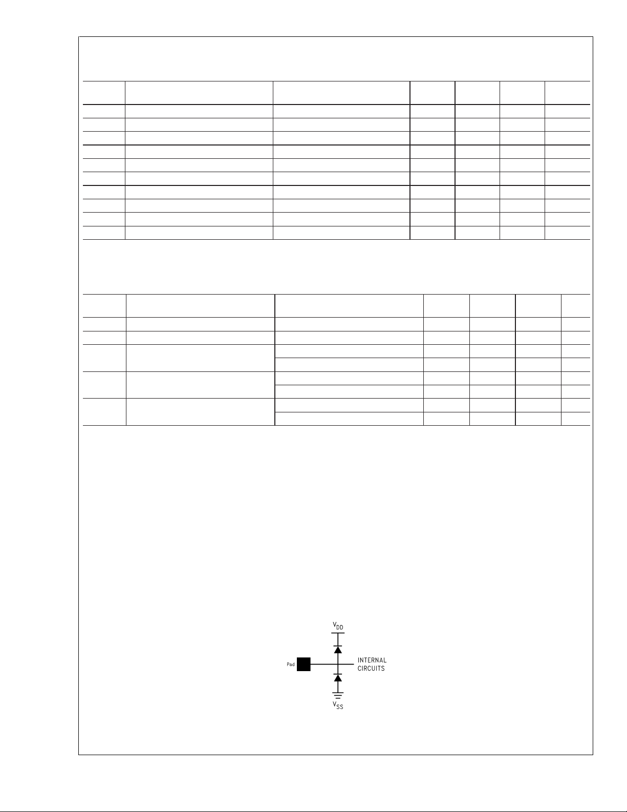
Note 7: The analog inputs are protected as shown below. Input voltage magnitude up to 500 mV beyond the supply rails will not damage this device. However, input
errors will be generated if the input goes above AV+ and below AGND.
DMAX
*
JA), and the ambient temperature (TA), and can be calculated using the formula P
=
1,811mW at 25˚C and 1,159 mW at the maximum operating ambient temperature of 70˚C. Note that the power dissipation of this
@
f
27 MHz 60 dB
CLK
=
@
f
20 MHz 61 dB
CLK
=
@
f
27 MHz 7.5 Bits
CLK
=
@
f
20 MHz 7.6 Bits
CLK
=
@
f
27 MHz −51 dB
CLK
=
@
f
20 MHz −60 dB
CLK
<
GND or V
IN
) for this device is 150˚C. The maximum allowable power dissipation is dictated by T
JMAX
>
AV+ or DV+), the current at that pin should be limited to 25 mA. The 50 mA
IN
=
27 MHz unless otherwise
CLK
Min
(Note 9)
Typical
(Note 8)
±
0.5 1.5 LSB
=
(T
DMAX
JMAX–TA
Max
(Note 9)
)/*JA. In the 48-pin
JMAX
Units
CLK
Units
, the
Note 8: Typical figures are at T
Note 9: Test limits are guaranteed to National’s AOQL (Averaging Outgoing Quality Level).
www.national.com 8
=
25˚C, and represent most likely parametric norms.
J
DS101292-18
 Loading...