

NSC LM9831CCVJD Datasheet
N
LM9831 42-Bit Color, 1200dpi USB Image Sc anner
General Description
The LM9831 is a complete USB image scanner system on a single IC. The LM9831 provides all the functions (image sensor
control, ill umination control, a nalog front end, pi xel processing
function image data buffer/DRAM controller, microstepping
motor cont rolle r, and USB i nterfac e) ne ces sary to create a high
performance color scanner. The LM9831 scans images in 42 bit
color/14 bit gray, and has output data formats for 24 bit color/8
bit gray. The LM9831 supports sensors with pixel counts of up to
16384 pixels x 3 colors (1200 dpi x 13.6 inches).
The LM9831’s low operating and suspend mode supply currents
allow design of USB bus-powered scanners. The only additional
active components required are an external 4Mbit or 16Mbit
DRAM for data buffering and power tra nsistors for the stepper
motor.
Applications
• Color Flatbed Document Scanners
• Color Sheetfed Document Scanners
Features
• 14 bit ADC digitizes at up to 6Mpixels/s (2M RGB pixels/sec).
• Digital Pixel Processing pr ovides 1200, 800, 600, 400, 300,
200, 150, and 100dpi horizontal resolution from a 1200dpi
sensor and 600, 400, 300, 200, 150, 100, 75, and 50dpi
horizontal resolution from a 600dpi sensor.
• Provides 50-2400dpi vertical resolution in 1 dpi increments.
• Pixel rate error correction for gain (shading) and offset errors.
• Supports 4 or 16Mbit external DRAMs.
• Multiple CCD clocking rates allows matching of CCD clock to
scan resolution and pixel depth for maximum scan speed.
• Stepper motor con trol tightly coupl ed with image data buffer
management to maximize data transfer efficiency.
• PWM stepper motor current c ontrol allows microst epping for
the price of fullstepping.
• USB interface for Plug and Play oper ation on USB- equipped
computers.
• Serial EEPROM option for custom Vendor and Product IDs.
• Support for USB bus-powered operation.
• Pixel depths o f 1, 2, or 4 bits are pac k ed into b yte s f or fas ter
scans of line art and low pixel depth images.
• Supports 3 channel CCDs and 1 channel CIS sensors.
• 3 (R, G, and B) 12-bit, user-programmable gamma correction
tables.
• Compatible with a wide range of color linear CCDs and
Contact Image Sensors (CIS).
• Operates with 48MHz external crystal.
• Internal bandgap voltage reference.
• 100 pin TQFP package
Key Specifications
• Analog to Digital Converter Resolution 14 Bits
• Maximum Pixel Conversion Rate 6MHz
• A4 Color 150dpi scan time <10 seconds
• A4 Color 300dpi scan time <40 seconds
• A4 Color 600dpi scan time <160 seconds
• Supply Voltage
- LM9831 +4.75V to +5.25V
- LM9831 DRAM I/O +2.85 to +5.25V
• Typical Operating Current Consumption 134mA
LM9831 42-Bit Color 1200dpi USB Image Scanner
October 1999
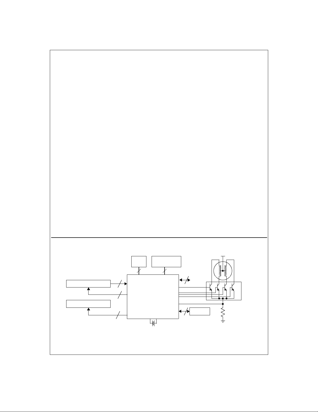
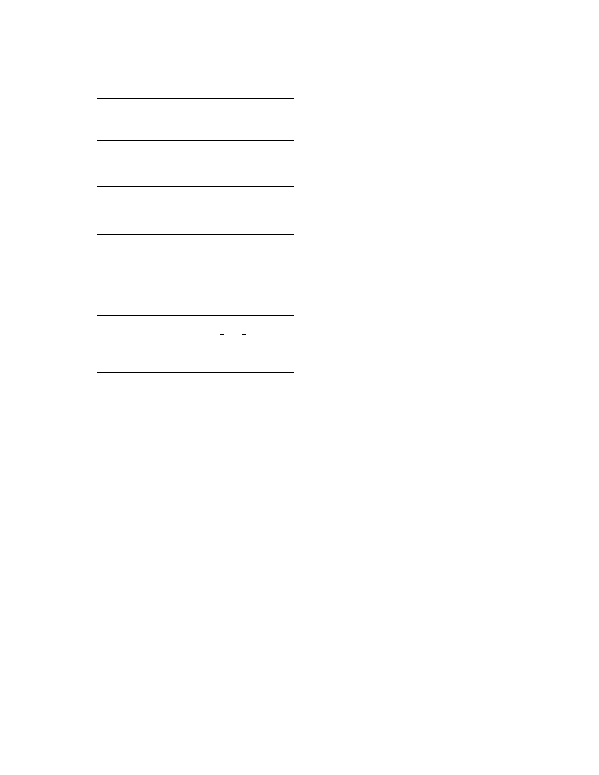
LM9831 Scanner System Block Diagram
USB
Port
2
2-6
1-3
1-3
LM9831CCVJD
CCD/CIS
Illumination
TRI-STATE® is a registered trademark of National Semiconductor Corporation.
©1999 National Semiconductor Corporation
Optional Serial
EEPROM
2
8MISC
I/O
30
DRAM
48MHz Crystal
1 www.national.com
+24V
Stepper
Motor
Power
Transistors
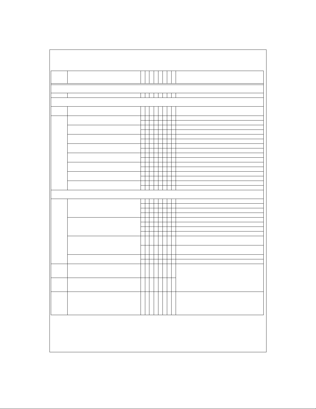
Absolute Maximum Ratings (Notes 1 & 2) Operating Ratings (Notes 1 & 2)
Positive Supply Voltage (V+=VA=VD=V
With Respect to GND=AGND=DGND 6.5V
Voltage On Any Input or Output Pin -0.3V to V
Input Current at any pin (Note 3) ±25mA
Package Input Current (Note 3) ±50mA
Package Dissipation at T
ESD Susceptibility (Note 5)
= 25°C (Note 4)
A
Human Body Model 2000 V
Machine Model 250 V
Soldering Information
Infrared, 10 seconds (Note 6) 235°C
Storage Temperature -65°C to +150°
DRAM
)
+
+0.3V
Operating Temperature Range T
LM9831VJD 0°C≤TA≤+70°C
Supply Voltage +4.75V to +5.25V
V
A
V
Supply Voltage +4.75V to +5.25V
D
Supply Voltage +2.85V ≤ V
V
DRAM
|V
| ≤ 100mV
A-VD
Input Voltage Range -0.05V to V
Electrical Characteristics
The following specifications apply for AGND=DGND=0V, VA=VD=V
f
CRYSTAL IN
= 48MHz.
Boldface limits apply for T
A=TJ=TMIN
to T
Symbol Parameter Conditions
Full Channel Characteristics (in units of 12 bit LSBs unless otherwise noted)
Resolution with No Missing Codes 14 12 bits (min)
DNL Differential Non-Linearity V
INL Integral Non-Linearity Error (Note 11) V
Analog Channel Gain Constant
C
(ADC Codes/V), referred to 14 bits.
V
V
V
Pre-Boost Analog Channel Offset Error 26
OS1
Pre-PGA Analog Channel Offset Error -30
OS2
Post-PGA Analog Channel Offset Error -26
OS3
DRAM
DRAM
Includes voltage reference
variation, gain setting = 1
Coarse Color Balance PGA Characteristics (Configuration Registers 3B, 3C, and 3D)
Monotonicity
G
(Minimum PGA Gain) PGA Setting = 0 0.93
0
G
(Maximum PGA Gain) PGA Setting = 31 3.00
31
x3 Boost Gain
x3 Boost Setting On
(bit B5 of Gain Register is set)
Gain Error at any gain (Note 13) 0.3
Static Offset DAC Characteristics (Configuration Registers 38, 39, and 3A)
Monotonicity
Offset DAC LSB size PGA gain = 1 9
Offset DAC Adjustment Range PGA gain = 1 ±278
=+5.0VDC,
DRAM
; all other limits TA=TJ=25°C. (Notes 8, 9, & 10)
MAX
Typical
(Note 9)
=3.3V
=3.3V
-0.47
+0.95
-3.2
+2.6
8192
2.94
DRAM
Limits
(Note 10)
-1
+2.4
-12.6
+7.3
7412
9300
-34
+76
-80
+31
-75
+26
5
0.90
0.96
2.95
3.05
2.85
3.04
-0.6
+0.9
6
6
12
±256
MIN≤TA≤TMAX
≤ VD+100mV
+
+ 0.05V
Units
(Limits)
LSB (min)
LSB (max)
LSB (min)
LSB (max)
LSB (min)
LSB (max)
mV (min)
mV (max)
mV (min)
mV (max)
mV (min)
mV (max)
bits (min)
V/V (min)
V/V (max)
V/V (min)
V/V (max)
V/V (min)
V/V (max)
% (min)
% (max)
bits (min)
mV (min)
mV (max)
mV (min)
2 www.national.com
Electrical Characteristics
The following specifications apply for AGND=DGND=0V, V
f
CRYSTAL IN
= 48MHz.
Boldface limits apply for T
(Continued)
A=TJ=TMIN
A=VD=VDRAM
to T
=+5.0VDC,
; all other limits TA=TJ=25°C. (Notes 8, 9, & 10)
MAX
Symbol Parameter Conditions
CCD/CIS Source Requirements for Full Specified Accuracy and Dynamic Range (Note 12)
V
CCDPEAK
Sensor’s Maximum Output Signal
Amplitude before LM9831 Analog Front
End Saturation
Gain = 0.933
Gain = 3. 0
Gain = 9.0
Analog Input C haracteristics
Average OS
OS
R
, OSG, OSB Input Current CDS Enabled, OS = 3.5V
R
, OSG, OSB Input Current CDS Disabled, OS = 3.5V
DC
DC
Internal Voltage Reference Characteristics
V
BANDGAP
V
REF LO
V
REF MID
V
REF HI
V
REGULA-
TOR
Voltage Reference Output Voltage 1.23 V
Negative Reference Output Voltage
Midpoint Reference Output Voltage
Positive Reference Output Voltage
USB I/O Voltage Regulator
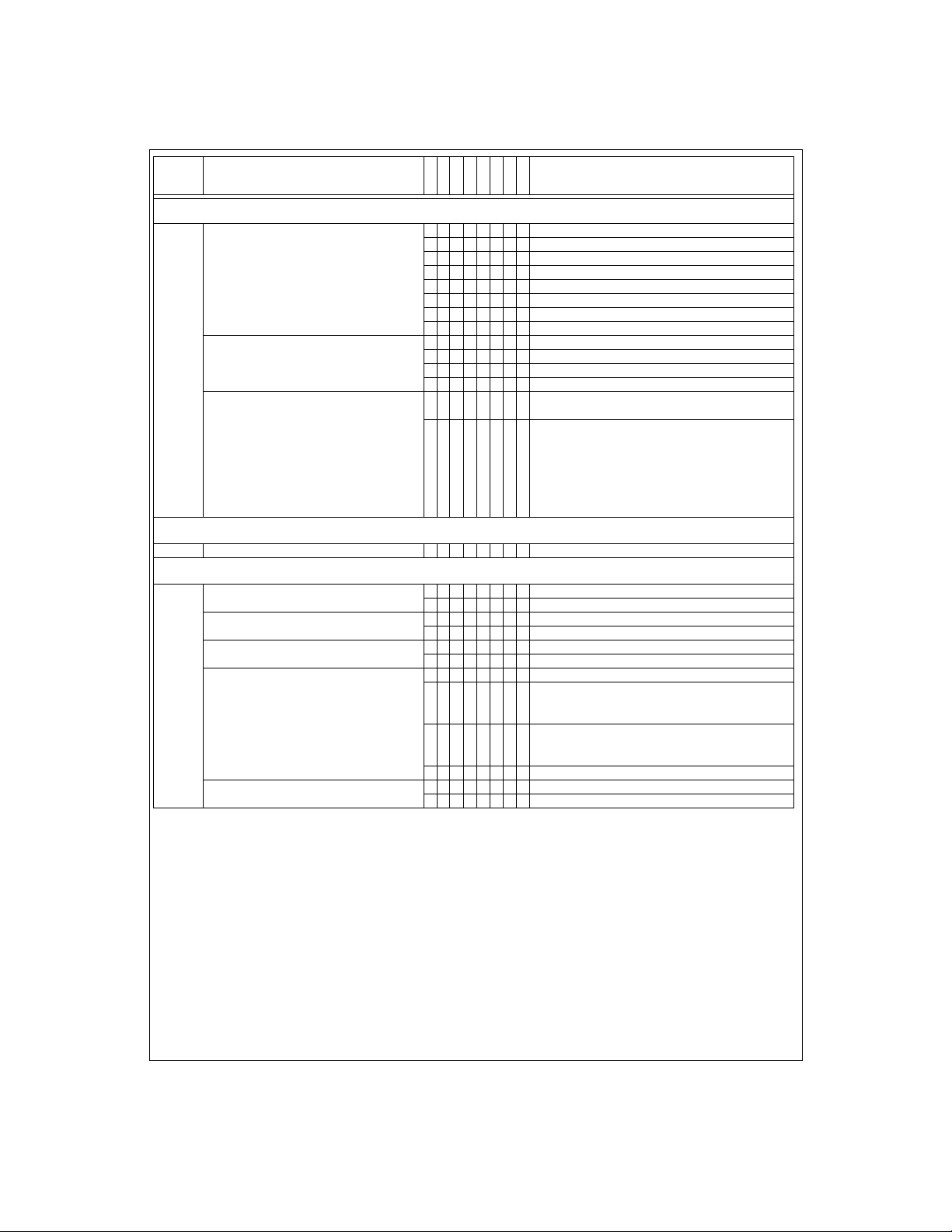
DC and Logic Electrical Characteristics
The following specifications apply for AGND=DGND=0V, VA=VD=V
f
CRYSTAL IN
= 48MHz.
Boldface limits apply for T
A=TJ=TMIN
to T
Symbol Parameter Conditions
Digital Input Characteristics for D0-D15 (DRAM Interface)
V
V
V
C
Logical “1” Input Voltage
IN(1)
Logical “0” Input Voltage
IN(0)
I
Input Leakage Current ±0.1 µA
IN
Input Capacitance 5 pF
IN
V
V
V
DRAM
DRAM
DRAM
DRAM
Digital Input Characteristics for PAPER SENSE 1-2, MISC I/O 1-6, SDA, BUS POWER
CMODE
V
V
C
Logical “1” Input Voltage VD=5.25V
IN(1)
Logical “0” Input Voltage VD=4.75V
IN(0)
I
Input Leakage Current ±0.1 µA
IN
Input Capacitance 5 pF
IN
Digital Input Characteristics for D+, D-
V
V
C
Logical “1” Input Voltage VD=5.25V
IN(1)
Logical “0” Input Voltage VD=4.75V
IN(0)
I
Input Leakage Current ±0.1 µA
IN
Input Capacitance 5 pF
IN
=+5.0VDC unless otherwise noted,
DRAM
; all other limits TA=TJ=25°C. (Notes 8, 9, & 10)
MAX
=5.25V
=3.6V
=4.75V
=2.85V
, CRY STAL/EXT CLOCK, 24/48, RESET,
Typical
(Note 9)
Limits
(Note 10)
1.9
0.6
0.19
±3 nA
±26
-1.0 V
V
REF MID
/2.0 V
V
A
+1.0 V
V
REF MID
3.4
Typica l
(Note 9)
±30
Limits
(Note 10)
2.0
2.0
0.8
0.8
2.0
0.8
2.0
0.8
Units
(Limits)
V
V
V
µA (max)
V
Units
(Limits)
V (min)
V (min)
V (max)
V (max)
V (min)
V (max)
V (min)
V (max)
3 www.national.com
DC and Logic Electrical Characteristics
The following specifications apply for AGND=DGND=0V, V
f
CRYSTAL IN
= 48MHz.
Boldface limits apply for T
A=TJ=TMIN
(Continued)
A=VD=VDRAM
to T
=+5.0VDC unless otherwise noted,
; all other limits TA=TJ=25°C. (Notes 8, 9, & 10)
MAX
Symbol Parameter Conditions
Digital Output Characteristics for D0-D15, A0-A9, RD
V
OUT(1)
V
OUT(0)
Digital Output Characteristics for A, B, A
V
OUT(1)
V
OUT(0)
Logical “1” Output Voltage
Logical “0” Output Voltage
, B
Logical “1” Output Voltage
Logical “0” Output Voltage
, WR, RAS, CAS (DRAM Interface)
V
V
V
V
V
V
V
V
DRAM
DRAM
DRAM
DRAM
DRAM
DRAM
DRAM
DRAM
=4.75V, I
=2.85V, I
=4.75V, I
=2.85V, I
=4.75V, I
=2.85V, I
=4.75V, I
=2.85V, I
OUT
OUT
OUT
OUT
OUT
OUT
OUT
OUT
=-4mA
=-4mA
=4mA
=4mA
=-10mA
=-10mA
=4mA
=4mA
Digital Output Characteristics for MISC I/O 1-6, TR1, TR2, ø1, ø2, RS, CP1, CP2, LAMP
V
V
OUT(1)
OUT(0)
Logical “1” Output Voltage VD=4.75V, I
Logical “0” Output Voltage VD=4.75V, I
OUT
OUT
=-4mA
=4mA
Digital Output Characteristics for D+, D-
V
V
OUT(1)
OUT(0)
Logical “1” Output Voltage VD=4.75V, I
Logical “0” Output Voltage VD=4.75V, I
OUT
OUT
=-1mA
=3mA
CRYSTAL IN, CRYSTAL OUT Characteristics
XTAL
XTAL
CRYSTAL OUT Bias Level (Offset) 0.8 V
OUT DC
CRYSTAL OUT Amplitude f
OUT AC
= 48MHz 0.8 V
CRYST AL
Power Supply Cha racteristics
I
I
I
DRAM
Analog Supply Current
A
(V
A
Digital Supply Current
D
(V
D
DRAM Supply Current
(V
DRAM
pins)
pins)
pins)
Operating
Suspend
Operating
Suspend (including I
Operating, V
Operating, V
Suspend
DRAM
DRAM
DRAM
= 5V
= 3V
)
Typica l
(Note 9)
, LAMPG, LAMP
R
87
1
37
14
10
5
14
Limits
(Note 10)
2.4
2.4
0.4
0.4
2.4
2.4
0.4
0.4
B
2.4
0.4
2.4
0.4
137
50
21
14
Units
(Limits)
V (min)
V (min)
V (max)
V (max)
V (min)
V (min)
V (max)
V (max)
V (min)
V (max)
V (min)
V (max)
P-P
mA (max)
µA (max)
mA (max)
µA (max)
mA (max)
mA (max)
µA (max)
4 www.national.com
AC Electrical Ch ar acterist ic s
The following specifications apply for AGND=DGND=0V, VA=VD=V
f
CRYSTAL IN
C
= 48MHz, MCLK DIVIDER = 1.0 (unless otherwise noted), f
(databus loading) = 20pF/pin.
L
Boldface limits apply for T
A=TJ=TMIN
Symbol Parameter Conditions
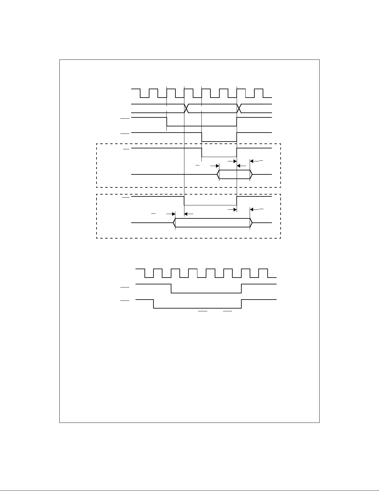
DRAM Timing (Figure 1)
V
=5.0V
t
RD SETUP
t
RD HOLD
t
WR SETUP
t
WR HOLD
Note 1:
Absolute Maximum Ratings indicat e limits beyond which damage to the device may occur. Operating Ratings indicat e conditions for which the device is functional,
but do not guarantee specific performance limits. For guaranteed speci fications and test conditions, see the Elec trical Characteristics. The guaranteed specifications apply
only for the test cond itions listed. Some performance characteristics may degrade when the device is not operated under the listed test conditions.
Note 2:
All voltages are measured with respect to GND=AGND=DGND =0V, unless otherwise specified.
Note 3:
When the input voltage (V
maximum package input current rating limits the number of pins that can simultaneously safely exceed the power supplies with an input c urrent of 25mA to two.
Note 4:
The maximum power dissipati on must be derated at elevated temperatures and is dictated by T
able power dissipation at any temperature is P
.
is 53°C/W
Note 5:
Human body model, 100pF capacitor discharged through a 1.5kΩ resistor. Machine model, 200pF capacitor discharged through a 0Ω resistor.
Note 6:
See AN-45 0 “Sur fa ce M oun tin g Met hod s a nd T hei r E ffect o n Pro duct Reliab ility” o r the sectio n titled “Su rfa ce Mount” found in any N ational Semiconductor Linear
Data Book for other methods of soldering surface mount devices.
Note 7:
Two diodes clamp the OS analog inputs to
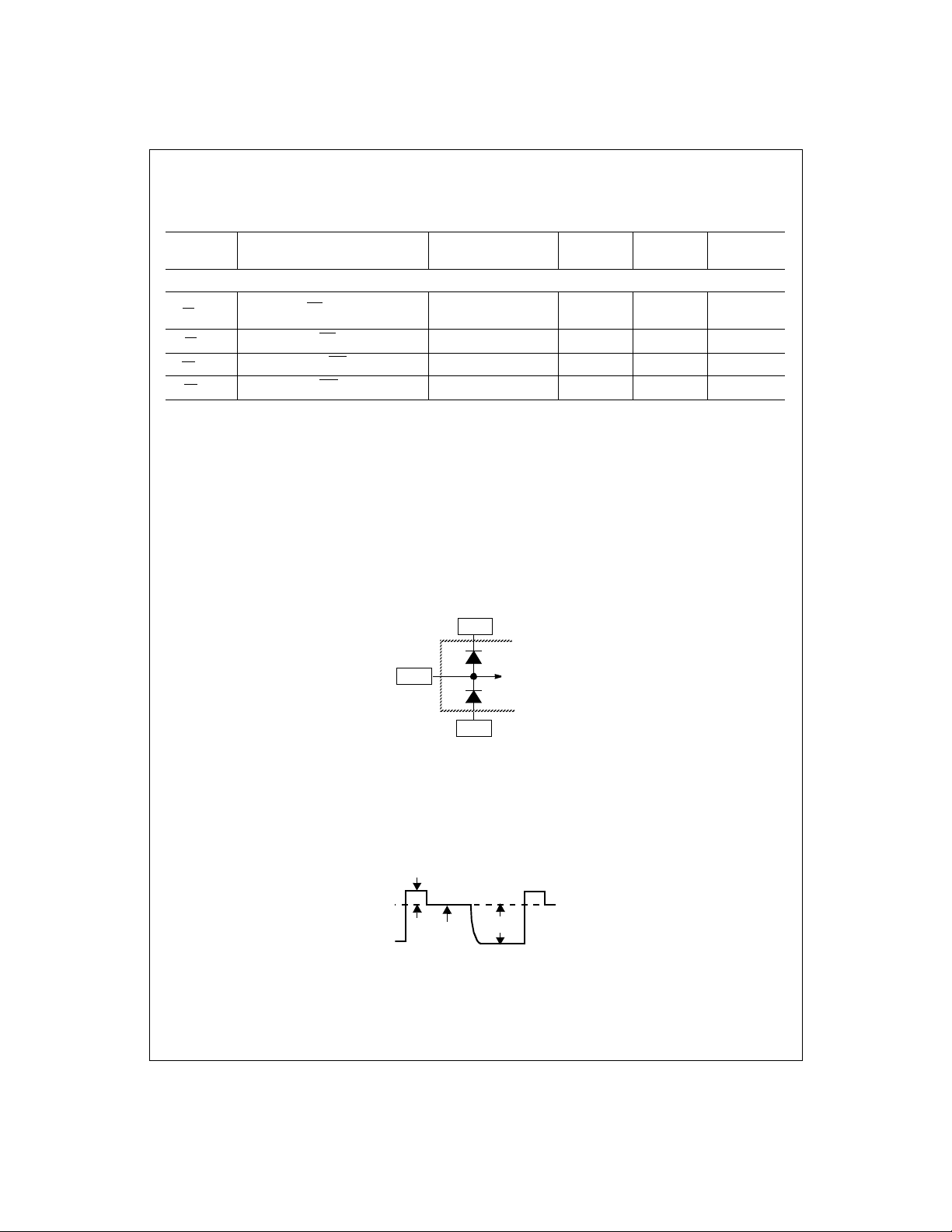
impedance of the sensor, prevents damage to the LM9831 from transients during power-up.
Data valid to RD rising edge
Data valid after RD rising edge
Data valid before WR falling edge
Data valid after WR rising edge
) at any pin exceeds the power supplies (VIN<GND or VIN>VA or VD), the current at that pin should be limited to 25mA. The 50mA
IN
= (TJmax - TA) /
D
AGND
and VA as shown below. This input protection, in combination with the external clamp capacitor and the output
DRAM
V
=3.3V
DRAM
Θ
. TJmax = 150°C for this device. The typical thermal resistance (
JA
VA
=+5.0VDC unless otherwise noted,
DRAM
MCLK
to T
= f
CRYSTAL IN
MAX
/MCLK DIVIDER, f
; all other limits TA=TJ=25°C. (Notes 8, 9, & 10)
Typical
(Note 9)
Θ
max,
and the ambient temperature, TA. The maximum allow-
J
JA
= f
ADC CLK
Limits
(Note 10)
26
35
0
5
10
Θ
) of this part when board mounted
JA
Units
(Limits)
ns (min)
ns (min)
ns (min)
ns (min)
ns (min)
MCLK
/8,
OS Input
To Internal
Circuitry
AGND
Note 8:
For best performance, it is required that all supply pins be powered from the same power supply with separate bypass capaci tors at each supply pin.
Note 9:
Typicals are at T
Note 10:
Tested limits are guaranteed to National's AOQ L (Average Outgoing Quality Level).
Note 11:
Integr al linearity error is def ined as the devi ation of the analog value, expressed in LSBs, from the straight line that best fits the actual transfer function of the ADC.
Note 12:
V
is defined as the CCD OS voltage for the reference period following the reset feedthrough pulse. V
REF
a white (full scale) image with respect to the reference level, V
correctable range of pixel-to-pixel V
LM9831 can correct for using its internal PGA.
Note 13:
PGA Gain Error is the maximum difference between the measured gain for any PGA code and the ideal gain calculated by using the formula
V
--- -
PGA
V
G0X
Gain
=25°C, f
J=TA
WHITE
PGA code
--------------- ----------- -+=XG
where .
32
= 48MHz, and represent most likely parametric norm.
CRYSTAL IN
.
is defined as the peak positive deviation above V
V
REF
variation is defined as the maximum variation in V
–
()
31G0
RFT
V
RFT
V
32
----- -=
31
CCD Output Signal
V
REF
WHITE
is defined as the peak CCD pixel output voltage for
WHITE
of the reset feedthrough pulse. The maximum
(due to PRNU, light source intensity variation, optics, etc.) that the
WHITE
REF
5 www.national.com
Timing Diagrams
48MHz Internal Clock
(t
= 20.83ns)
PERIOD
A0-A9 Row Address
RAS
CAS
RD
Read Operation
WR
Write Operation
01234560
n
Column Address
t
RD SETUP
n
Row Address
t
RD HOLD
n+1
DataD0-D15
t
t
WR SETUP
WR HOLD
DataD0-D15
Figure 1: DRAM Read and Write
48MHz Internal Clock
(t
= 20.83ns)
PERIOD
RAS
CAS
01234560
Figure 2: DRAM Refresh (CAS
before RAS)
6 www.national.com
Connection Diagram
V
BANDGAP
V
REF LO
V
REF MID
V
REF HI
AGND
V
DGND
OS
OS
OS
V
D0
D15
DRAM
D1
D14
D2
D13
D3
D12
D4
D11
AGND VADGND VDTEST SENSEGND SENSEA SENSEB NC CMODE RESET NC NC DGND VDBUS POWR D+ D- V
10099 98 97 96 95 94 93 92 91 90 89 88 87 86 85 84 83 82 81 80 79 78 77 76
1
2
3
R
4
5
G
6
7
B
8
9
A
A
10
A
11
B
12
B
13
14
LM9831VJD
15
16
17
18
19
20
21
22
23
24
25
26 27 28 29 30 31 32 33 34 35 36 37 38 39 40 41 42 43 44 45 46 47 48 49 50
REGULATOR
DGND ACTIVE/SUSPENDED CP2 CP1 RS ø2
75
74
73
72
71
70
69
68
67
66
65
64
63
62
61
60
59
58
57
56
55
54
53
52
51
ø1
TR2
TR1
MISC I/O 6
MISC I/O 5
MISC I/O 4
DGND
V
MISC I/O 3
MISC I/O 2
MISC I/O 1
D
PAPER SENSE 1
PAPER SENSE 2
V
D
DGND
LAMP
B
LAMP
G
LAMP
R
DGND
V
D
24/48
CRYSTAL
CRYSTAL IN
/EXT
CRYSTAL OUT
SCL
CLK
D5
D6
D9
D10
Ordering Information
Commercial (0°C ≤ TA ≤ +70°C) Package
LM9831CCVJD VJD100A 100 Pin Thin Quad Flatpac
LM9831CCVJDX VJD100A 100 Pin Thin Quad Flatpac, Tape and Reel
D7
D8
WR
DRAM
DGND
V
CAS
A9A8A0A7A1
RD
RAS
A6A2A5A3A4
DRAM
DGND
V
SDA
7 www.national.com
Pin Descriptions
g
USB Interface
D+, D- Digital I/O. USB Interface signals
BUS POWER
ACTIVE/
SUSPENDED
SDA Digital I/O. Serial Data to/from external
SCL Digital Output. Serial Clock Output to external
Digital Input. Tie low for bus powered systems, tie high for external power.
Digital Output. Low in Suspend mode. High in
operational mode. Used to control external
regulators, other components.
EEPROM.
EEPROM.
Analo
OSR,
OS
,
G
OS
B
V
REF LO
V
REF MID
V
REF HI
V
BANDGAP
V
REGULATOR
Analog Inputs. These i nputs (for Red, Green,
and Blue) should be tied to the sensor’s output signal th rough DC blocking capacitors. If
unused, tie to ground through DC blocking
capacitors.
Analog Output/Input. Bypass to AGND with a
0.047µF monolithic capacitor. Do not put a
DC load on this pin.
Analog Output/Input. Bypass to AGND with a
0.047µF monolithic capacitor. Do not put a
DC load on this pin.
Analog Output/Input. Bypass to AGND with a
0.047µF monolithic capacitor. Do not put a
DC load on this pin.
Analog Output. Bypass to AGND with a
0.047µF monolithic capacitor. Do not put a
DC load on this pin.
Analog Output. Bypass to AGND with a
0.047µF monolithi c capacitor. Used as terminal voltage for 1.5k D+ pullup resistor.
DRAM
D0 (LSB) -D15
(MSB)
RD
WR
A0-A9 Di gital Outputs. Address pins for up to 1M x
RAS
CAS
Digital Inputs/Outputs. This is the 16 bit data
path between the external DRAM and the
LM9831.
Digital Output. Read signal to external DRAM.
Digital Output. Write signal to external DRAM.
16 external DRAM.
Digital Output. Row Address Strobe signal.
Digital Output. Column Address Strobe sig-
nal.
Scanner Support I/O
PAPER
SENSE 1-2
MISC I/O 1-6 Digital Inputs/Outputs. Programmable, used
Digital Inputs. Programm able, used for sensing home position, paper, front panel
switches, etc.
for front panel switches, status LE Ds, etc. At
power-on and in Suspend Mode, MISC I/Os
1-3 are inputs and MISC I/Os 4-6 are outputs.
Stepper Motor
A, B, A, B Digital Outputs. Pulses to stepper motor drive
SENSE
A
SENSE
B
SENSE
GND
circuitry.
,
Analog Inputs. Current sensing for stepper
motor’s PWM current co ntrol.
Analog Input. G round se nse input for s tepper
motor’s PWM current co ntrol.
Sensor Control
ø1 Digital Output. CCD/CIS clock signal phase 1.
ø2 Digital Output. CCD/CIS clock signal phase 2.
RS Digital Output. Reset pulse for the CCD/CIS.
CP1 Digital Output. Clamp pulse for the CCD/CIS.
CP2 Digital Output. Clamp pulse for the CCD/CIS.
TR1, TR2 Digital Outputs. Transfer pulses for the
,
LAMP
R
LAMP
,
G
LAMP
B
CCD/CIS.
Digital Output s. Used to cont rol R, G, and B
LEDs of single output CIS, as wel l as brightness of CCFL. The CDS signal can b e seen
on LAMP
7).
in a test mode (see register 5E, bit
B
Master Clock Generation
CRYSTAL IN Digital Input. Used with CRYSTAL OUT and
CRYSTAL
OUT
CRYSTAL
EXT CL OCK
24/48
an external 48MHz crystal to form a crystal
oscillator.
Digital Output. Used with CRYSTAL IN and an
external 48MHz crystal to form a crystal oscillator.
/
Digital Input. Tie to DGND for operation wi th
an external crystal. Pull up to V
CRYSTAL OUT with an external TTL or
CMOS clock source.
Digital Input. Tie to DGND for operation with a
48MHz crystal or external clock. Pull up to V
for operation with a 24MHz crystal or external
clock. NOTE: Operation at 24MHz is not guaranteed - always use a 48MHz crystal.
to drive
D
D
8 www.national.com
Miscellaneous
RESET Digital input. Ta ke high to force device into
TEST Analog Output.
CMODE Digital Input. Test mode, always tie high.
Power On Reset state, low to exit reset state.
Analog Power Supplies (4 pins)
VA (2) This is the positive supply pin for the analog
AGND (2) This is the ground r eturn for the analog sup -
supply. It should be connected to a v oltage
source of +5V and bypassed to AGND with a
0.1µF monolithic capacitor in parallel with a
10µF tantalum capacitor.
ply.
Digital Power Supplies (17 pins)
VD (5) This is the positive supply pin for the digital
(3) This is the po sitive supply pi n for the digital
V
DRAM
DGND (9) This is the ground return for V
supply. It should be connected to a v oltage
source of +5V and by passed to D GND wi th a
0.1µF monolithic capacitor.
supply for the LM9831’s external DRAM I/O. It
also powers the A, B, A
outputs. It should be connected to a 3 or 5V
supply and bypassed to the closest DGND pin
with a 0.1µF monolithic capacitor.
, and B stepper motor
and V
D
DRAM
.
9 www.national.com
LM9831 Register Listing
Registers in bold boxes are reset to that value on power-up. All register addresses are in hexadecimal. All other numbers are
decimal unless otherwise noted.
Address Function
IMAGE BUFFER (READ ONLY)
00
Pixel (Image) D ata
STATUS REGISTERS (READ ONLY)
01
Image Data Available In Buffer
PAPER SENSE 1 State
read clears bit if edge sensitive input.
PAPER SENSE 2 State
read clears bit if edge sensitive input.
MISC I/O 1 State
read clears bit if edge sensitive input.
MISC I/O 2 State
read clears bit if edge sensitive input.
02
MISC I/O 3 State
read clears bit if edge sensitive input.
MISC I/O 4 State
read clears bit if edge sensitive input.
MISC I/O 5 State
read clears bit if edge sensitive input.
MISC I/O 6 State
read clears bit if edge sensitive input.
DATAPORT REGISTERS
DataPort Target
DataPort Targ et Color
03
Pause (Read Only)
This bit indicates whether or not the scanner
is currently paused due to a buffer full
condition.
DRAM Test
04
DataPort Address - MSB
05
DataPort Address - LSB
06
nnnnnnnn
DataPort
D7D6D5D4D3D2D1D
n n n n n n n n One byte of image data.
nnnnnnnn
0False
1True
0False
1True
0False
1True
0False
1True
0 Normal State
1 The scanner is currently in the pause/reverse cycle.
0 Normal Operation
1 DRAM Test mode
R
/Waaaaaa
aaaaaaaa
0
n*2 (256k x 16 DRAM) or n*8 (1M x 16 DRAM)
kilobytes of image data is available
0False
1True
0False
1True
0False
1True
0False
1True
0 0 Offset Coefficient Data
0 1 Gain Coefficient Data
1 0 Gamma Lookup Table
11N/A
00 Red
0 1 Green
10 Blue
11 N/A
Address of location to be read/written to.
a = 0 to 4095 for gamma tables,
0 to 16383 for Offset and Gain Coefficient Data
Addresses greater than these are illegal.
Bit D6 of register 4 indicates whether next operation
will be a Read (D6=1) or a Write (D6=0)
Data to be read from or written to the address of the
currently selected Dataport Target. The DataPort
Address is automatically incremented whenever one
(gamma data) or two (Gain/Offset Data) bytes are
read from or written to this register.
Value
.
10 www.national.com
Address Function
COMMAND REGISTER
Command Register
This register is used to start and end a scan.
It is also used to home the sensor in a
flatbed scanner or eject the image in a
sheetfed scanner.
Note: Always make sure
the Command Register is in the idle state
(=0) before issuing a new command.
07
Standby
When this bit is set the entire chip enters a
low power state.
Warning: A Standby command will stop
DRAM refresh.
Reset
Write a 1 then a 0 to reset the LM9831’s
state machines.
Warning: A Reset will stop DRAM refresh.
MASTER CLOCK DIVIDER
MCLK Divider
This register sets the master clock frequency
for the entire scanner.
08
f
= 48MHz/MCLK_Divider
MCLK
f
= f
MCLK
/8
ADC
D7D6D5D4D3D2D1D
0
Idle - Stops motor (A, B, A
000
completes current line of data (if scanning).
Note: CCD/CIS clocks continue clocking.
High Speed Forward - Moves motor forward at a
001
speed determined by the Fast Feed Step Size
(registers 48 and 49).
High Speed Reverse - Moves motor backward at a
010
speed determined by the Fast Feed Step Size
(registers 48 and 49).
Start Scan - Resets the LM9831’s data pointers and
011
starts an image scan.
Programmed High Speed Forward - Moves motor
forward at a speed determined by the Fast Feed Step
101
Size (registers 48 and 49) for the number of lines
programmed in registers 4A and 4B.
Programmed High Speed Reverse - Moves motor
backward at a speed determined by the Fast Feed
110
Step Size (registers 48 and 49) for the number of lines
programmed in registers 4A and 4B.
0 Normal Operation
1 Low Power Standby Mode
0 Normal Operation
1 Resets the LM9831
000000÷1.0
000001÷1.5
000110÷4
a a a a a a ÷ ((aaaaaa/2)+1)
111110÷32.0
111111÷32.5
Value
, B = 0),
11 www.national.com
Address Function
HORIZONTAL RESOLUTION AND DA TAMODE SETTINGS
Horizontal DPI Divider
This register determines the horizontal
resolution of the scan.
Scan resolution = Optical resolution divided
by the Horizontal_DPI_Divider.
Pixel Packing
This register determines how many bits in
09
each byte of data are transmitted to the host
when DataMode = 0
DataMode
When DataMode = 0, the pixel data is fully
processed, going through the Offset,
Shading, Horizontal DPI Adjust, Gamma,
and Pixel Packing blocks.
When DataMode = 1, 14 bit data is extracted
following the Shading Multiplier stage.
Gamma and any other post processing must
be done by the host.
RESERVED
0A Reserved 0 0 0 0 0 0 0 0 Write 00 to this register
SENSOR CONFIGURATION
Input Signal Polarity
CDS On/Off
Standard/Even-Odd Senso r
0B
CIS TR1 Timing Mode
Fake Optical Black Pixels
(for Dyna-type CIS sensors)
D7D6D5D4D3D2D1D
0 0 1 bit/pixel (1 bit grayscale/3 bit color)
0 1 2 bits/pixel (2 bit grayscale/6 bit color)
1 0 4 bits/pixel (4 bit grayscale/12 bit color)
1 1 8 bits/pixel (8 bit grayscale/24 bit color)
0
1
0 0 Off - use standard CCD Timing
01
10
11 N/A
0 Off: Normal operation
1 On: RS pulse held high for entire Optical Black period
0
000÷1
001÷1.5
010÷2
011÷3
100÷4
101÷6
110÷8
111÷12
1, 2, 4, or 8 bit image data,
as determined by the Pixel Size setting.
14 bit image data - sent in 2 bytes, MSB first:
First Byte: 13 12 11 10 09 08 07 06
Second Byte: 05 04 03 02 01 00 XX XX
(XX: bits set to 0)
0 Negative (Most CCD Sensors and Toshiba CIS)
1 Positive (Most CIS Sensors)
0 CDS Off
1 CDS On
0 Standard (1 pixels per Ø period)
1 Even/Odd (2 pixels per Ø period)
CIS TR1 Timing Mode 1:
TR1 pulse = exactly one Ø clock,
starting at rising edge of Ø1
CIS TR1 Timing Mode 2:
TR1 pulse = exactly one Ø clock,
TR1 centered around Ø1 high.
Value
12 www.national.com
Address Function
SENSOR CONTROL SETTINGS
Ø1 Polarity
Ø2 Polarity
RS Polarity
0C
CP1 Polarity
CP2 Polarity
TR1 Polarity
TR2 Polarity
Ø1 Active/Off
Ø2 Active/Off
RS Active/Off
CP1 Active/Off
0D
CP2 Active/Off
TR1 Active/Off
TR2 Active/Off
Number of TR Pulses
TR Pulse Duration
0E
TR-Ø1 Guardband Duration
0F
Optical Black Clamp Start
10
Optical Black Clamp End
11
Rese t Pulse Start
12
Reset Pulse Stop
13
CP1 Pulse Start
14
CP1 Pulse Stop
15
CP2 Pulse Start
16
CP2 Pulse Stop
17
Reference Sample Position
18
Signal Sample Position
INTEGRATION TIME ADJUST
19
Integration Time Adjustment Function
STEPPER PHASE CORRECTION
1A
TR to Stepper Phase Correction - MSB
1B
TR to Stepper Phase Correctio n - LSB
D7D6D5D4D3D2D1D
0
Value
0Positive
1 Negative
0Positive
1 Negative
0Positive
1 Negative
0Positive
1 Negative
0Positive
1 Negative
0Positive
1 Negative
0Positive
1 Negative
0Off
1Active
0Off
1Active
0Off
1Active
0Off
1Active
0Off
1Active
0Off
1Active
0Off
1Active
01 TR Pulse
12 TR Pulses
n n n n n+1 pixel periods (1-16)
n n n n n pixel periods (0-15)
nnnnn
nnnnn
nnnnn
nnnnn
nnnnn
nnnnn
nnnnn
nnnnn
nnnnn
nnnnn
nnnnnnnt
pixel rate: n=0-23, line rate: n=0-7 MCLKs from Ø1 edge
pixel rate: n=0-23, line rate: n=0-7 MCLKs from Ø1 edge
pixel rate: n=0-23, line rate: n=0-7 MCLKs from Ø1 edge
pixel rate: n=0-23, line rate: n=0-7 MCLKs from Ø1 edge
pixel rate: n=0-23, line rate: n=0-7 MCLKs from Ø1 edge
pixel rate: n=0-23, line rate: n=0-7 MCLKs from Ø1 edge
pixel rate: n=0-23, line rate: n=0-7 MCLKs from Ø1 edge
pixel rate: n=0-23, line rate: n=0-7 MCLKs from Ø1 edge
pixel rate: n=0-23, line rate: n=0-7 MCLKs from Ø1 edge
pixel rate: n=0-23, line rate: n=0-7 MCLKs from Ø1 edge
= n*t
READOUT
, n = 1 to 127. n=0 turns off function.
INT
First step of scan occurs n pixels (1 - 16383) after first
nnnnnn
TR pulse. This register can be used to set the phase
between the TR pulses and the stepper motor pulses.
NOTE: a setting of n = 0 creates the maximum delay
nnnnnnnn
(16384) pixels, which will increase scan time. If this
function is not used, this register should be set to 1.
13 www.national.com
 Loading...