

NSC LM9830VJD Datasheet
N
LM9830 36-Bit Color Document Scanner
General Description
The LM9830 is a complete docu ment s canner syst em on a single IC. The LM9830 provides all the functions (CCD control, illumination control, analog front end, pixel processing function
image data buffer/SRAM controller, microstepping motor controller, and EPP parallel por t interface) necessar y to create a high
performance color scanne r. The LM9830 scans images i n 36 bit
color, and has output data formats for 36 bits, 30 bits, and 24
bits.
The only additional a ctive components requ ired are an exter nal
SRAM for data buffering and power transist ors for the stepper
motor. Parallel port pass-through requires two additional
TTL/CMOS logic ICs.
Applications
•
Color Flatbed Document Scanners
•
Color Sheetfed Document Scanners
Features
• Scans at up to 6Mpixels/s (2M RGB pixels/sec).
• Digital Pixel Processing provides 300, 200, 150, 10 0, 75, and
50 dpi horizontal resolution from 300dpi sensor, and 600, 400,
300, 200, 150, 100, 75, an d 50 dpi hor izontal resol ution from
a 600dpi sensor.
• Provides 50-600dpi vertical resolution in 1 dpi increments.
• Pixel rate error correction for gain (shading) and offset errors.
• Output formats inclu de 12 bit linear, 10 bit linear with shad ing
and offset, or 8 bit gamma corrected, all with 12 bit accuracy.
• Multiple CCD clocking rates allows matching of CCD clock to
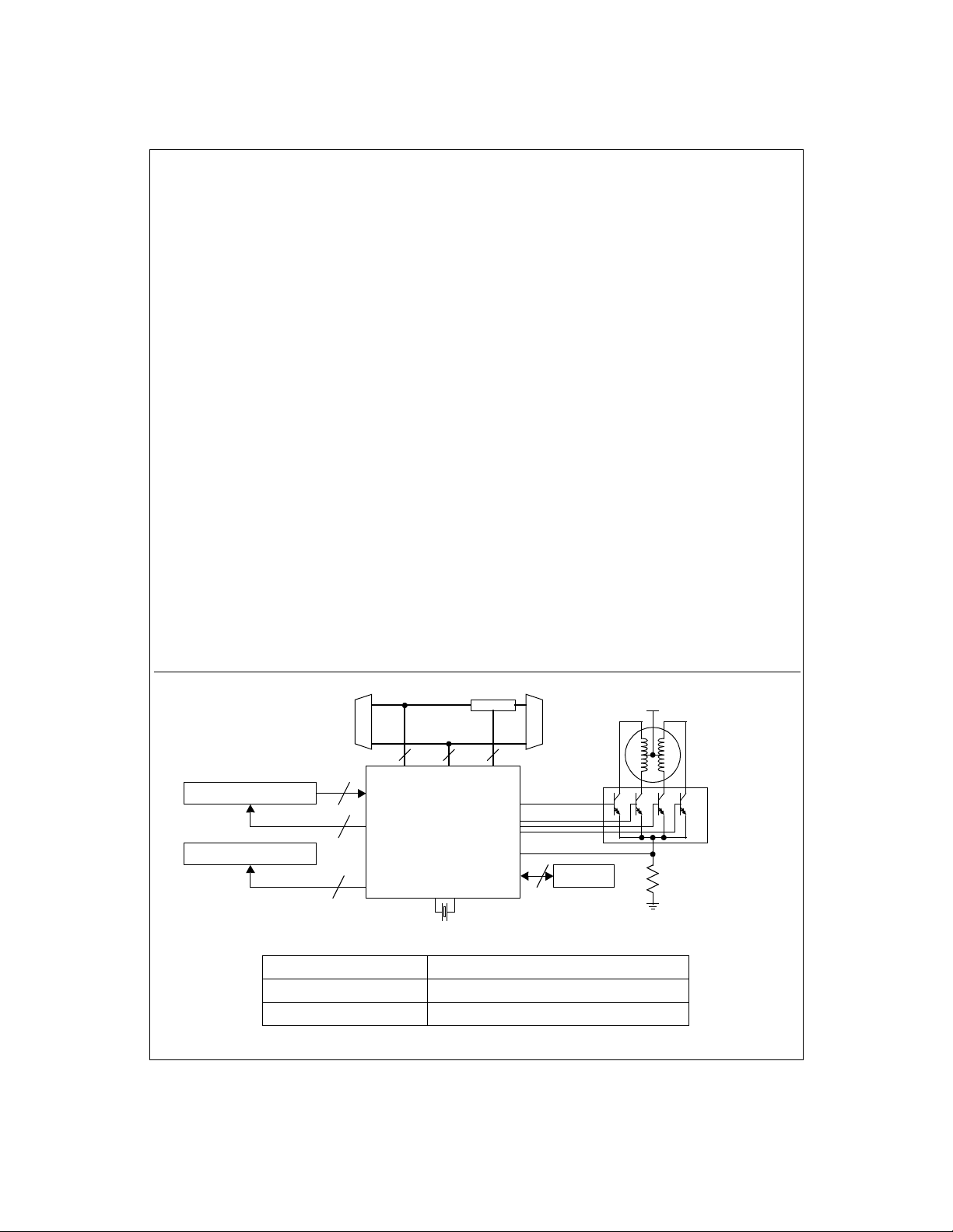
Scanner Block Diagram
To
Computer
CCD/CIS
2-6
Illumination
1-3
DB25
9 28
1-3
LM9830VJD
scan resolution and pixel depth for maximum scan speed.
• Stepper motor control tightly coupled with buffer management
to maximize data transfer efficiency.
• PWM stepper motor curr ent control allows microsteppi ng for
the price of fullstepping.
• Supports 64k, 128k, or 25 6k x8 external SRAMs.
• Parallel Port interface suppor ts EPP, PS2 (bidirection al), or
SPP (nibble) modes of operation.
• Pixel depths of 1, 2, or 4 bits are packed into bytes for faster
scans of line art and low pixel depth images.
• Supports 1 and 3 channel CIS and CCD devices.
• 3 (R, G, and B) user-programmable gamma correction tables.
• Able to transmit an arbitrary range of pixels to speed up
scanning of smaller items (business cards, etc. ) by zooming
in on a subset of CCD pixels.
• Compatible with a wide range of color linear CCDs and
Contact Image Sensors (CIS)
• Internal bandgap voltage reference.
• 100 pin TQFP package
Key Specifications
•
Analog to Digital Converter Resolution 12 Bits
•
Maximum Pixel Conversion Rate 6MHz
•
A4 Color 150dpi scan (typical, EPP Interface) <10 seconds
•
A4 Color 300dpi scan (typical, EPP Interface) <40 seconds
•
A4 Color 600dpi scan (typical, EPP Interface) <160 seconds
•
Supply Voltage +5V±10%
•
Power Dissipation (typical) 350mW
Buffer
DB25
Printer
28
To
SRAM
+24V
November 1998
Stepper
Motor
Power
Transistors
LM9830 36-Bit Color Document Scanner
Ordering Information
Commercial (0°C ≤ TA ≤ +70°C) Package
LM9830VJD VJD100A 100 Pin Thin Quad Flatpac
LM9830VJDX VJD100A 100 Pin Thin Quad Flatpac, Tape & Reel
TRI-STATE® is a registered trademark of National Semiconductor Corporation.
©1998 National Semiconductor Corporation
1
http://www.national.com
(
)
Absolute Maximum Ratings
Positive Supply V oltage (V+=VA=VD=V
With Respect to
GND=AGND=DGND=DGND
V oltage On Any Input or Output Pin -0.3V to V
=DGND
I/O
DI/O=VSRAM
SRAM
(Notes 1 & 2)
)
+
+0.3V
Input Current at any pin (Note 3) ±25mA
Package Input Current (Note 3) ±50mA
Package Dissipation at T
ESD Susceptibility (Note 5)
= 25°C (Note 4)
A
Human Body Model 1000V
Operating Ratings
Operating Temperature Range T
LM9830VJD 0°C≤T
6.5V
V
Supply Voltage +4.5V to +5.5V
A
V
Supply Voltage +4.5V to +5.5V
D
V
Supply Voltage +4.5V to +5.5V
DI/O
|V
|, |VA-V
A-VD
|V
D-VSRAM
Input Voltage Range -0.05V to V
DI/O
|, |V
DI/O-VSRAM
|, |VA-V
Soldering Information
Infrared, 10 seconds (Note 6) 235°C
Storage T emperature -65°C to +150°
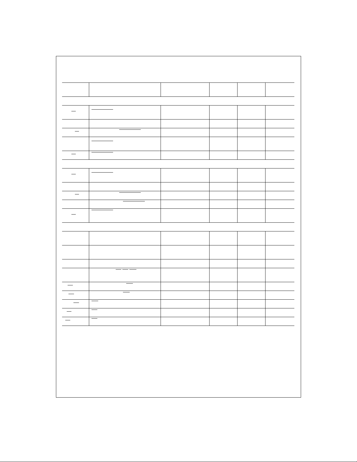
Electrical Characteristics
The following specifications apply for AGND=DGND=DGND
f
CRYSTAL IN
= 50MHz. Boldface limits apply for T
A=TJ=TMIN
Symbol Parameter Conditions
CCD/CIS Source Requirements for Full Specified Accuracy and Dynamic Range
Sensor’s Maximum Output Signal
V
OS
Amplitude before LM9830 Analog Front
PEAK
End Saturation
Full Channel Characteristics
Resolution with No Missing Codes 12 bits (min)
INL Integral Non-Linearity Error
(Note 11)
DNL Differential Non-Linearity
Analog Channel Gain Constant
C
(ADC Codes/V)
V
V
V
V
Pre-Boost Analog Channel Offset Error,
OS1
CCD Mode
Pre-Boost Analog Channel Offset Error,
OS1
CIS Mode
Pre-PGA Analog Channel Offset Error -30
OS2
Post-PGA Analog Channel Offset Error -21
OS3
Coarse Color Balance PGA Characteristics (Configuration Registers 3B, 3C, and 3D)
Monotonicity 5 bits (min)
(Minimum PGA Gain) PGA Setting = 0 0.93
G
0
(Maximum PGA Gain) PGA Setting = 31 3.05
G
31
x3 Boost Gain
Gain Error at any gain
(Note 13)
I/O
to T
=DGND
MAX
=0V, VA=VD=V
SRAM
; all other limits TA=TJ=25°C. (Notes 7, 8, & 12)
Gain = 0.933
Gain = 3.0
Gain = 9.0
Includes voltage reference
variation, gain setting = 1
x3 Boost Setting On
(bit B5 of Gain Register is set)
Note 12
(Notes 1 & 2)
|, |VD-V
SRAM
|,
DI/O=VSRAM
Typical
(Note 9)
|,
DI/O
=+5.0VDC,
Limits
(Note 10)
2.1
0.65
0.21
-1.1
+4.6
-0.5
+0.7
2048
4
12
-7
+10
-0.9
+2.0
1863
2129
-21
+34
-15
+38
-58
+8
-59
+14
.90
.96
2.98
3.15
2.99
2.86
3.08
±0.2 ±1.6 % (max)
≤
T
MIN
A
≤
100mV
+
+ 0.05V
LSB (min)
LSB (max)
LSB (min)
LSB (max)
LSB (min)
LSB (max)
mV (min)
mV (max)
mV (min)
mV (max)
mV (min)
mV (max)
mV (min)
mV (max)
V/V (min)
V/V (max)
V/V (min)
V/V (max)
V/V (min)
V/V (max)
≤
T
A
MAX
≤
+70°C
Units
(Limits)
V
V
V
2
http://www.national.com
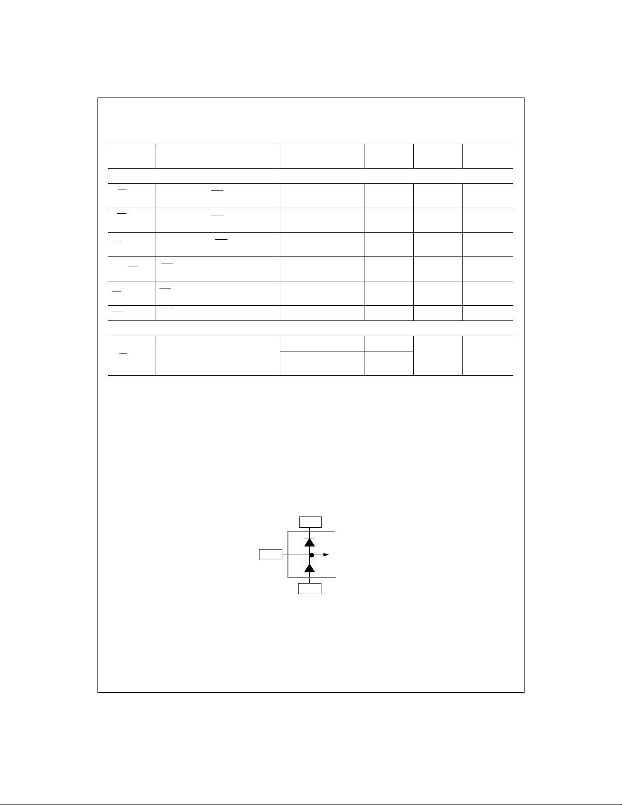
Electrical Characteristics
The following specifications apply for AGND=DGND=DGND
f
CRYSTAL IN
= 50MHz.
Boldface limits apply for T
(Continued)
A=TJ=TMIN
I/O
to T
=DGND
MAX
=0V, VA=VD=V
SRAM
; all other limits TA=TJ=25°C. (Notes 7, 8, & 12)
Symbol Parameter Conditions
Static Offset DAC Characteristics (Configuration Registers 38, 39, and 3A)
Monotonicity
Offset DAC LSB size PGA gain = 1 9.3
Offset DAC Adjustment Range PGA gain = 1 ±290
Analog Input Characteristics
Average OS
OS
R
, OSG, OSB Input Current CDS Enabled, OS = 3.5V
R
, OSG, OSB Input Current
CDS Disabled,
OS = 3.5V
Internal Voltage Reference Characteristics
V
BANDGAP
V
REF LO
V
REF MID
V
Voltage Reference Output Voltage 1.2 V
Negative Reference Output Voltage
Midpoint Reference Output Voltage
Positive Reference Output Voltage
REF HI
DC and Logic Electrical Characteristics
The following specifications apply for AGND=DGND=DGND
f
CRYSTAL IN
= 50MHz.
Boldface limits apply for T
A=TJ=TMIN
Symbol Parameter Conditions
Digital Input Characteristics for DB0-DB7, D0-D7, STROBE
#1, MISC I/O #2, CMODE
V
V
C
Logical “1” Input Voltage V
IN(1)
Logical “0” Input Voltage V
IN(0)
Input Leakage Current ±500 nA
I
IN
Input Capacitance 5 pF
IN
Digital Output Characteristics for DB0-DB7, A0-A17, RD
V
V
OUT(1)
OUT(0)
Logical “1” Output Voltage V
Logical “0” Output Voltage V
Digital Output Characteristics for D0-D7, ERROR
V
V
OUT(1)
OUT(0)
Logical “1” Output Voltage V
Logical “0” Output Voltage V
Digital Output Charact er ist ics for MI SC I/O #1 , M IS C I /O #2, A, B, A
LAMP
, LAMPG, LAMP
V
V
R
OUT(1)
OUT(0)
Logical “1” Output Voltage V
Logical “0” Output Voltage V
B
I/O
to T
=DGND
MAX
=0V, VA=VD=V
SRAM
; all other limits TA=TJ=25°C. (Notes 7 & 8)
, AUTOFEED, INIT, SELECT IN, PSENSE#1, PSENSE#2, MISC I/O
=5.5V
DI/O
=4.5V
DI/O
, WR (SRAM Interface)
DI/O
DI/O
=4.5V, I
=5.5V, I
OUT
OUT
=-4mA
=8mA
, ACK, BUSY, PE, SELECT (Parallel Port Interface)
DI/O
DI/O
=4.5V, I
=5.5V, I
OUT
OUT
=-4mA
=14mA
, B, TR1, TR2, ø1, ø2, RS, CP1, CP 2, TRI STATE, LATCH,
DI/O
DI/O
=4.5V, I
=5.5V, I
OUT
OUT
=-4mA
=8mA
DC
DC
DI/O=VSRAM
=+5.0VDC,
Typical
(Note 9)
(Note 10)
±80 nA
±24
V
-1.0 V
REF MID
V
/2.0 V
A
V
+1.0 V
REF MID
DI/O=VSRAM
=+5.0VDC,
Typical
(Note 9)
(Note 10)
Limits
6
5.8
12.7
±270
±30
Limits
2.0
0.8
2.4
0.4
2.4
0.4
2.4
0.4
Units
(Limits)
bits (min)
mV (min)
mV (max)
mV (min)
µA (max)
Units
(Limits)
V (min)
V (max)
V (min)
V (max)
V (min)
V (max)
V (min)
V (max)
3
http://www.national.com
DC and Logic Electrical Characteristics
The following specifications apply for AGND=DGND=DGND
f
CRYSTAL IN
= 50MHz.
Boldface limits apply for T
A=TJ=TMIN
Symbol Parameter Conditions
CRYSTAL IN, CRYSTAL OUT Characteristics
XTAL
XTAL
CRYSTAL OUT Bias Level (Offset) 0.8 V
OUT DC
CRYSTAL OUT Amplitude f
OUT AC
Power Supply Characteristics
Analog Supply Current
I
A
(V
pins)
A
I
D I/O
Digital I/O Supply Current
(V
, VD, and V
D I/O
SRAM
pins)
=DGND
I/O
to T
CRYSTAL
SRAM
; all other limits TA=TJ=25°C. (Notes 7 & 8)
MAX
= 50MHz 0.8 V
Operating
Standby
Operating
Standby
AC Electrical Characteristics
The following specifications apply for AGND=DGND=DGND
f
CRYSTAL IN
C
= 50MHz, MCLK DIVIDER = 1.0 (unless otherwise noted), f
(databus loading) = 20pF/pin.
L
Boldface limits apply for T
Symbol Parameter Conditions
Parallel Port Address Write (Figure 1)
t
SETUP1
t
SETUP2
t
SI-B1
t
B-SI
t
HOLD1
t
SI-B2
t
HOLD2
D0-D7 (Address) valid to SELECT IN
falling
STROBE falling edge to SELECT IN
falling
SELECT IN falling to BUSY rising 25
BUSY rising to SELECT IN rising 0
SELECT IN rising to STROBE rising -45
SELECT IN rising to BUSY falling 33
D0-D7 (Address) hold time after
BUSY falling
Parallel Port Data Write (Figure 2)
t
SETUP1
t
SETUP2
t
AF-B1
t
B-AF1
t
HOLD1
t
AF-B2
t
HOLD2
D0-D7 valid or STROBE falling to
SELECT IN
falling
STROBE falling to A UT OFEED falling -25
AUTOFEED falling to BUSY rising 34
BUSY rising to AUTOFEED rising 0
AUTOFEED rising to STROBE rising -40
AUTOFEED rising to BUSY falling
D0-D7 valid after BUSY falling -10
=DGND
I/O
A=TJ=TMIN
SRAM
MCLK
to T
All Except Dataport
Dataport
=0V, VA=VD=V
DI/O=VSRAM
=+5.0VDC,
Typical
(Note 9)
(Note 10)
64
0.75
40
5
=0V, VA=VD=V
= f
CRYSTAL IN
; all other limits TA=TJ=25°C. (Notes 7 & 8)
MAX
DI/O=VSRAM
/MCLK DIVIDER, f
Typical
(Note 9)
-60
-15
=+5.0VDC,
Limits
(Note 10)
-10
-10
40
20
-15
50
-10
-60
0
-10
-10
50
20
-10
1.5 t
16
ADC CLK
3 t
ADC CLK
35
0
Limits
83
0.95
48
6.5
ADC CLK
Units
(Limits)
mA (max)
mA (max)
mA (max)
mA (max)
= f
MCLK
Units
(Limits)
ns (min)
ns (min)
ns (max)
ns (min)
ns (min)
ns (max)
ns (min)
ns (min)
ns (min)
ns (max)
ns (min)
ns (min)
ns (max)
ns (max)
ns (min)
P-P
/8,
4
http://www.national.com
AC Electri cal Characteristics
The following specifications apply for AGND=DGND=DGND
f
CRYSTAL IN
C
= 50MHz, MCLK DIVIDER = 1.0 (unless otherwise noted), f
(databus loading) = 20pF/pin.
L
Boldface limits apply for T
Symbol Parameter Conditions
Parallel Port 8 Bit Data Read (Figure 3)
t
AF-B3
t
EPP ACCESS
t
B-AF2
t
EPP HOLD
t
AF-B4
AUTOFEED falling to BUSY rising
D0-D7 valid before BUSY rising (Note 14) 7
BUSY rising to AUTOFEED rising 1
AUTOFEED rising to D0-D7 Tri-State 20
AUTOFEED rising to BUSY falling 3 t
Nibble Data Read (Figure 4)
t
AF-B3
t
NIB ACCESS1
t
B-AF2
t
NIB ACCESS2
t
AF-B4
AUTOFEED falling to BUSY rising
D4-D7 valid before BUSY rising 2
BUSY rising to AUTOFEED rising 1
D0-D3 valid after AUT OFEED rising 5
AUTOFEED rising edge to BUSY
falling
Microprocessor Mode (Figures 5, 6, and 7)
t
ALE SETUP
t
ALE HOLD
t
ALE
t
ALE-R/W
t
WR SETUP
t
WR HOLD
t
WR
t
RD ACCESS
t
RD TRI-STATE
D0-D7 (Address) valid before ALE
falling
D0-D7 (Address) valid after ALE
falling
ALE high time 2
ALE falling to CS/RD/WR falling (next
operation)
D0-D7 valid before WR rising 0
D0-D7 valid after WR rising 2
WR pulse width 3
RD low to D0-D7 valid 22
RD high to D0-D7 Tri-State 20
=DGND
I/O
A=TJ=TMIN
All Except Dataport
Dataport
All Except Dataport
Dataport
=0V, VA=VD=V
SRAM
= f
MCLK
CRYSTAL IN
to T
; all other limits TA=TJ=25°C. (Notes 7 & 8)
MAX
DI/O=VSRAM
/MCLK DIVIDER, f
Typical
(Note 9)
(Note 10)
25
1.5 t
ADC CLK
MCLK
3 t
4 t
25
1.5 t
ADC CLK
3 t
MCLK
3 t
4 t
0
2
=+5.0VDC,
ADC CLK
Limits
45
ADC CLK
-5
10
10
27
MCLK
45
ADC CLK
-20
10
15
MCLK
6
8
8
16
6
10
10
31
28
= f
MCLK
Units
(Limits)
ns (max)
ns (max)
ns (min)
ns (min)
ns (min)
ns (max)
ns (max)
ns (max)
ns (max)
ns (min)
ns (min)
ns (max)
ns (max)
ns (min)
ns (min)
ns (min)
ns (min)
ns (min)
ns (min)
ns (min)
ns (max)
ns (max)
/8,
5
http://www.national.com
AC Electri cal Characteristics
The following specifications apply for AGND=DGND=DGND
f
CRYSTAL IN
C
= 50MHz, MCLK DIVIDER = 1.0 (unless otherwise noted), f
(databus loading) = 20pF/pin.
L
Boldface limits apply for T
Symbol Parameter Conditions
SRAM Write Timing (Figure 8) - Typical Values Represent Worst Case Timing for Different MCLK Frequencies
t
WR F ADDR
SETUP
t
WR R ADDR
SETUP
t
WR DATA SETUP
t
WR
t
WR ADDR HOLD
t
WR DATA HOLD
Address valid to WR falling
Address valid to WR rising
DB0-DB7 valid to WR rising
WR pulse width
WR rising to Address data change
WR rising to DB0-DB7 data Tri-State 1
SRAM Read Timing (Figure 9) - Typical Values R epresent Worst Case Timing for Different MCLK Frequenc ies
t
RD SETUP
Note 1: Absolute Max im um Ratings indicate limit s beyond w hic h damage to the device may occu r. Operating R atings indicate condit ions for which the device is functional,
but do not guarantee specific perform ance limits. For guarantee d specifications an d t est conditions, see t he Electrical Cha rac teristics. The guaranteed specifications apply
only for the test condition s list ed. Some performance c haracteristics may degrade w hen the device is not operated un der the listed test conditions.
Note 2: All voltages are measured with respect to GND=AGND=DGND=DGND
Note 3: When the input voltage (V
imum package input cur rent rating limits the numbe r of pins t hat can simultaneously sa fely exceed t he power supplies with an input current of 25mA to two.
Note 4: The ma xi mu m power dissipation mus t be derated at elevated temperatures and is dictated by T
able power dissipation at any temperature is P
is 53°C/W
.
Note 5: Human body m odel, 100pF capacitor discharged throug h a 1. 5kΩ resistor.
Note 6: See AN450 “Surface M ount ing M et hods and T heir Effect o n Pro duct Re liabilit y” o r the sect ion t itled “Surface M oun t” found in any Nation al Semic onducto r Linear
Data Book for other methods of soldering surface mount devices.
Note 7: Two diodes clamp the OS analog inputs to
impedance of the sensor, prevents damage to the LM9830 fro m tran s ients during power-up.
Address valid to DB0-DB7 data valid
) at any pin exceeds the power supplies (VIN<GND or VIN>VA or VD), the current at that pin should be limited to 25mA. The 50mA max-
IN
= (TJmax - TA) / ΘJA. TJmax = 150°C for this device. The typical thermal resistance (ΘJA) of this part when board m ounted
D
AGND
and VA as shown below. This input protection, in com bination with the external clamp cap ac it or and the output
=DGND
I/O
A=TJ=TMIN
=0V, VA=VD=V
SRAM
= f
MCLK
CRYSTAL IN
to T
; all other limits TA=TJ=25°C. (Notes 7 & 8)
MAX
4 slot mode 2 t
8 slot mode
= 25MHz)
(f
MCLK
I/O
=DGND
=0V, unless otherwis e s pec ified.
SRAM
VA
max, ΘJA and the ambient temperat ure, TA. The maximum allow-
J
DI/O=VSRAM
/MCLK DIVIDER, f
Typical
(Note 9)
0.5 t
MCLK
- 7ns
1.5 t
MCLK
- 9ns
1 t
MCLK
- 9ns
1 t
MCLK
- 5ns
0.33 t
MCLK
- 4ns
- 12ns
MCLK
1 t
- 12ns
MCLK
=+5.0VDC,
Limits
(Note 10)
3
21
11
15
2
4
28
ADC CLK
= f
MCLK
Units
(Limits)
ns (min)
ns (min)
ns (min)
ns (min)
ns (min)
ns (max)
ns (max)
/8,
AGND
6
T o In te rnal
Circuitry
is defined as the peak CCD pixel output voltage for
WHITE
of the reset feedthrough pulse. The maximum
(due to PRNU, light so urce intensity var iation, optics, et c.) that the
WHITE
REF
http://www.national.com
OS Input
Note 8: For best performanc e, it is required that all supply pin s be powered from the same power su pply with separate bypass capacitors at each supply pin.
Note 9: Typicals are at T
Note 10: Tested limits are guaranteed to Natio nal's AOQL (Average Outgoing Quality Level).
Note 11: Integral linearity error is defined as the deviation of the analog value, expressed in LSBs, from the straight line that best fits the actual transfer function o f th e ADC.
Note 12: V
a white (full scale) image with respect to the reference level, V
correctable range of pixel-to-pixel V
is defined as the CCD OS voltage for the reference period following the reset feedthrough pulse. V
REF
J=TA
=25°C, f
= 50MHz, and represent most likely parametric norm.
CRYSTAL IN
is defined as the peak positive deviation above V
. V
REF
variation is define d as the maximu m variation in V
WHITE
RFT
LM9830 can correct for using its internal PGA.
CCD Output Signal
V
RFT
V
Note 13: PGA Gain Error is the maximum difference between the measured gain for any PGA code and the ideal gain calculated by using the formula
V
Gain
--- -
PGA
V
Note 14: Interaction w it h an actual parallel po rt load (C
For this reason, it is recomme nded that the parallel port be driven to 0x00h by the PC w hen not in the reverse transfer phase. When readin g c oefficient data from regis t er 6
PGA code
G0X
-------------- ------------ -+=XG
where .
32
32
------=
–()
31G0
31
> 200pF) can increase data settling ti m e by as m uc h as 100ns if the para llel port databus is precharged high.
LOAD
V
REF
WHITE
(register 3 = 00000 XX1 bina r y), the EP P hands hakin g generat ed by the hos t PC may be faste r than the data ca n settle. For this reason it is recommended that software
handshaking (“PS2” mode) be used when verifying coefficient data.
7
http://www.national.com
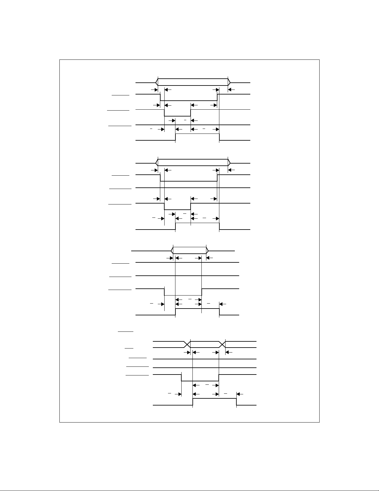
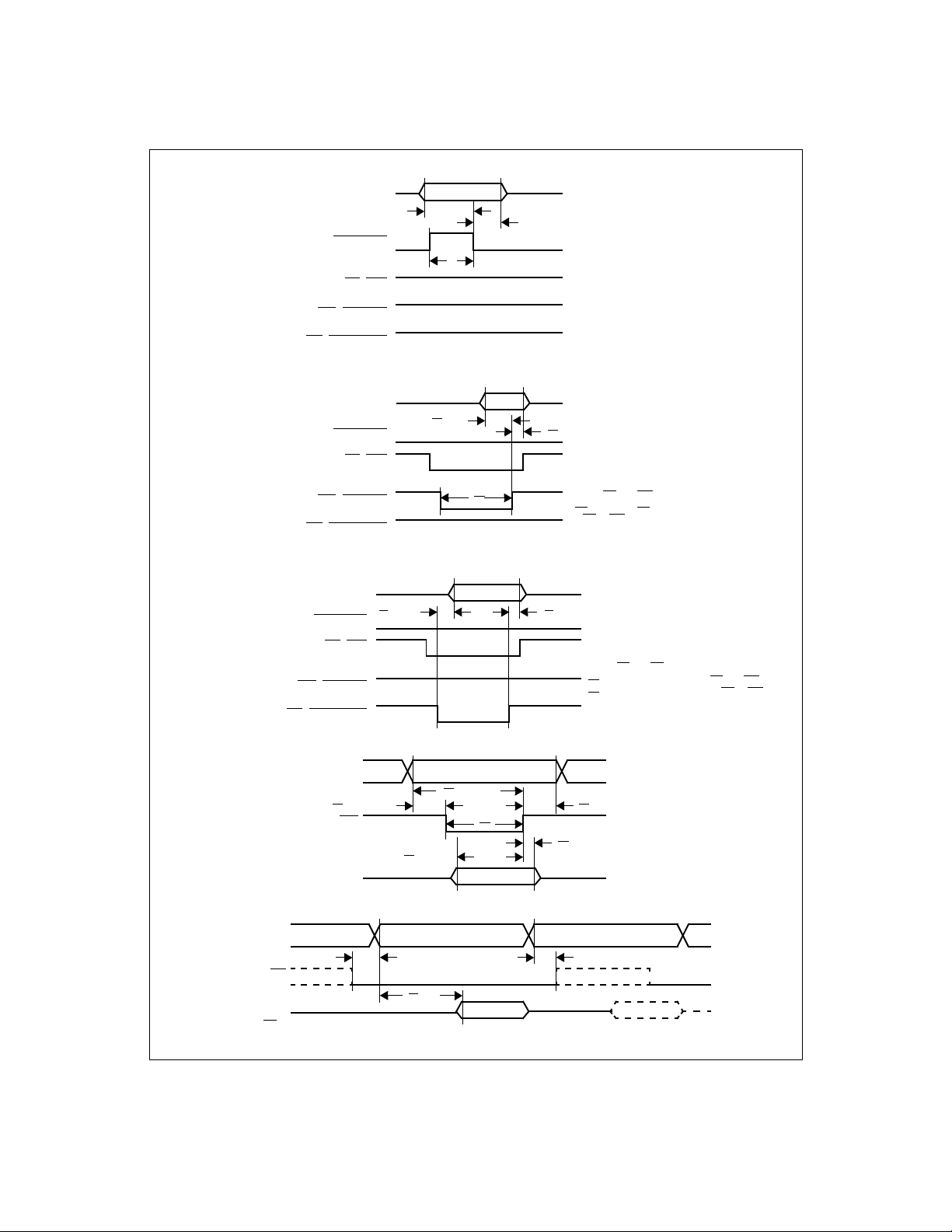
Timing Diagrams
D0 - D7
STROBE
SELECT IN
AUTOFEED
BUSY
D0 - D7
STROBE
SELECT IN
AUTOFEED
BUSY
D0 - D7
STROBE
Address
t
SETUP1
t
SETUP2
t
B-SI
t
SI-B1
Figure 1: Parallel Port Address Write
Data
t
SETUP1
t
SETUP2
t
t
AF-B1
B-AF1
Figure 2: Parallel Port Data Write
Data
t
EPP ACCESS
t
HOLD1
t
HOLD1
t
SI-B2
t
AF-B2
t
EPP HOLD
t
HOLD2
t
HOLD2
SELECT IN
AUTOFEED
BUSY
ERROR (D0, D4)
SELECT (D1, D5)
PE (D2, D6)
ACK
STROBE
SELECT IN
AUTOFEED
t
t
AF-B3
B-AF2
Figure 3: Parallel Port 8 Bit Data Read
(D3, D7)
t
NIB ACCESS1
t
AF-B3
BUSY
Figure 4: Parallel Port Nibble Data Read
8
t
AF-B4
D7-D4 D3-D0
t
NIB ACCESS2
t
B-AF2
t
AF-B4
http://www.national.com
D0 - D7
h
ALE (SELECTIN)
CS
(INIT)
WR (STROBE)
RD (AUTOFEED)
Address
t
ALE SETUP
t
ALE
t
ALE HOLD
Figure 5: µP Mode Address Latch
D0 - D7
ALE (SELECTIN)
CS (INIT)
WR (STROBE)
RD (AUTOFEED)
D0 - D7
ALE (SELECTIN)
(INIT)
CS
WR (STROBE)
RD (AUTOFEED)
A0-A17
t
WR F ADDR SETUP
WR
DB0-DB7
t
WR SETUP
Figure 6: µP Mode Write
t
RD ACCESS
Figure 7: µP Mode R ead
t
WR R ADDR SETUP
t
WR DATA SETUP
Figure 8: SRAM Write
Data
t
WR
Data
Address
t
WR
Data
t
WR HOLD
NOTE: CS and WR are ORed together.
t
and t
WR SETUP
of CS or WR, whichever goes high first.
t
RD TRI-STATE
WR HOLD
NOTE: CS and RD are ORed together.
t
begins when both CS and WR go low.
RD ACCESS
t
t
WR ADDR HOLD
t
WR DATA HOLD
RD TRI-STATE
begins when either CS or WR go hig
refer to the first rising edge
A0-A17
0.5MCLK 0.5MCLK
Address
RD
t
DB0-DB7
RD SETUP
Data
Note: RD will stay low during consecutive read operations.
Figure 9: SRAM Read
9
Address
Data
http://www.national.com
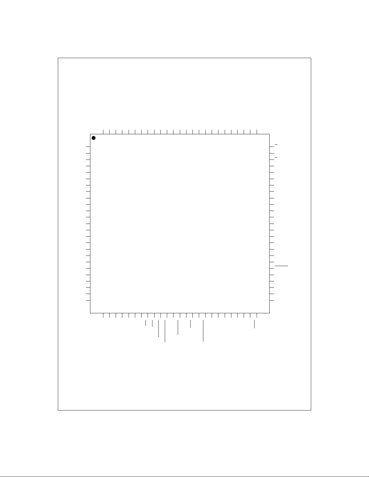
Connection Diagram
GND
V
DGND
V
DGND
A0
A1
A2
A3
A4
D I/O
A5
A6
A7
A8
A9
A10
A11
A12
A13
A14
A15
D I/O
A16
A17
DB0
DB1
DB2
CP2
CP1RSø2ø1TR2
VAOSBV
REF HI SENSEVREF HI FORCE
TR1
AGND
OSGV
REF MID SENSEVREF MID FORCE
OSRV
REF LO SENSEVREF LO FORCEVBANDGAP
AGND
VASENSE
SENSEBSENSEATEST
100999897969594939291908988878685848382818079787776
1
2
3
4
5
6
7
I/O
8
9
10
11
12
13
14
LM9830VJD
15
16
17
18
19
20
I/O
21
22
23
24
25
75
74
73
72
71
70
69
68
67
66
65
64
63
62
61
60
59
58
57
56
55
54
53
52
51
B
B
A
A
CLK_SEL
DGND
I/O
V
D I/O
CMODE
LAMP
B
LAMP
G
LAMP
R
MISC I/O #2
MISC I/O #1
PSENSE #2
PSENSE #1
DGND
SRAM
V
SRAM
CRYSTAL OUT
CRYSTAL IN
LATCH
NC
TRISTATE
SELECT
PE
BUSY
26 27 28 29 30 31 32 33 34 35 36 37 38 39 40 41 42 43 44 45 46 47 48 49 50
DB3
DB4
DB5
DB6
DB7
V
D
RD
DGND
WR
STROBE
AUTOFEED
D0
ERROR
10
D1
D3
V
D I/O
I/O
D4D5D6
D7
ACK
D2
INIT
DGND
SELECT IN
http://www.national.com
Pin Descriptions
CCD Driver Signals
ø1 Digital Output. CCD/ CIS clock signal, phase
ø2 Digital Output. CCD clock signal, phase 2.
RS Digital Output. Reset pulse for the CCD.
CP1 Digital Output. Clamp pulse for the CCD.
CP2 Digital Output. Clamp pulse for the CCD.
TR1, TR2 Digital Outputs. Transfer pulses for the
1.
CCD(CIS).
Analog I/O
OSR, OSG,
OS
B
V
REF LO FORCE,
V
REF LO SENSE
V
REF MID FORCE ,
V
REF MID SENSE
V
REF HI FORCE,
V
REF HI SENSE
V
BANDGAP
Analog Inputs. These in puts (for Red, Green,
and Blue) shou ld be tied to th e sensor’s output signal through DC blocking capacitors.
Analog Output/Input . Conne ct V
V
monolithic capacit or.
Analog Output/Input. Connect V
to V
0.05µF monolithic capacitor.
Analog Output/Inp ut. Connect V
V
monolithic capacit or.
Analog Output. Bypass to AGND with a
0.05µF monolithic capacitor.
and bypass to AGND with a 0.05µF
REF LO IN
REF MID IN
REF HI IN
and bypass to AGND with a
and bypass to AGND with a 0.05µF
REF LO OUT
REF MID OUT
REF HI OUT
General Digital I/O
CRYSTAL IN Digital Input. This is the 50MHz (typical) mas-
CRYSTAL OUT Digital Output. Used with CRYSTAL IN and an
CLK_SEL Digital Input. Should be tied to DGND for
ter system clock.
external crystal to form a crystal oscillator.
operation with an external cry stal. To use an
external TTL or CMOS clock source, tie
CLK_SEL to V
CRYSTAL OUT pin.
and driv e th e c lock into t h e
D I/O
PC I/O
D0 (LSB) -D7
(MSB)
STROBE
AUTOFEED
SELECTIN
INIT
ACK
BUSY Digital Output.
PE Digital Output.
SELECT Digital Output.
ERROR
Digital Inputs/Outputs. This is the 8 bit d ata
path between the LM9830 and the host computer.
Digital Input. WR signal in µP Mode.
Digital Input. RD signal in µP Mode.
Digital Input. ALE signal in µP Mode.
Digital Input. CS signal in µP Mode.
Digital Output.
Digital Output.
Printer Passthrough
TRISTATE Digital Output. Low when in printer
LATCH
passthrough mode, high when the LM9830 is
active. Low when no power is app lied to the
LM9830.
Digital Output. High when in printer
passthrough mode, low when th e LM9830 is
active. Tri-state when no power is applied to
the LM9830.
Stepper Motor I/O
A, B, A, B Digital Outputs. Pulses to stepper motor.
,
Analog Inputs. Current sensing for PWM
winding current control.
Analog Input. Ground sense input for PWM
winding current control.
Scanner Support I/O
Digital Inputs. Programmable, used for sensing paper, front panel switches, etc.
Digital Inputs/Outputs. Programmable, used
for front panel switches, status LEDs, etc.
Digital Outputs. Used to control R, G, and B
LEDs of single output CIS, as well as bright-
B
ness of CCFL.
to
to
SENSE
A
SENSE
B
SENSE
GND
PSense #1,
PSense #2
Misc I/O #1,
Misc I/O #2
,
LAMP
R
LAMP
, LAMP
G
External RAM I/O
DB0 (LSB) DB7 (MSB)
A0-A17 Digital Outputs. Add ress pins for up to 256k
RD
WR
Digital Inputs/Outputs. This is the 8 bit data
path between the external RAM and the
LM9830.
bytes external RAM.
Digital Output. Read signal to external RAM.
Digital Output. Write signal to external RAM.
Communication Mode
CMODE Digital Input. Tie to DGND to operate in paral-
lel port mode, or to V
processor c ompatible mode.
D I/O
Test
TEST Analog Output. This pin can be used to view
the Sample Signal, Sample Reference, and
Clamp Signals.
Analog Power Supplies
V
A
AGND This is the ground ret urn for the analog su p-
This is the positive supply pin for the analog
supply. It should be connected to a voltage
source of +5V and bypassed to AGND with a
0.1µF monolithic c apacitor in parallel with a
10µF tantalum capacitor.
ply.
to operate in micro-
11
http://www.national.com
Digital Power Supplies
V
D
DGND This is the ground return for V
V
D I/O
DGND
I/O
V
SRAM
DGND
SRAM
This is the positive supply pin for the
LM9830’s digital circuitry. It should be connected to a voltage source of +5V and
bypassed to DGND with a 0.1µF monolithic
capacitor.
.
D
This is the positive supply pin for the
LM9830’s external I/O. It should be connected
to a +5V voltage source and bypassed to the
closest DGND
capacitor.
This is the ground return for V
pin with a 0.1µF mo nolithic
I/O
.
D I/O
This is the positive supply pin for the
LM9830’s internal SRAM sense amplifiers
and crystal o scillator. It should be connected
to a +5V voltage source and bypassed to
DGND
This is the ground return for V
with a 0.1µF monolithic capacitor.
SRAM
D SRAM
.
Other
NC Do Not Connect. This pin should be left float-
ing.
12
http://www.national.com
LM9830 Register Listing
(Registers in bold boxes are reset to t hat value on power-up. All register addre sses are in hexadec imal. All other numbers
are decimal unless otherwi se noted.)
Address Function
IMAGE BUFFER (READ ONLY)
00 Pixel (Image) Data nnnnnnnnOne byte of image data.
STATUS REGISTERS (READ ONLY)
01 Image Data Available In Buffer nnnnnnnn
Paper Sensor #1 State
If this input is edge sensitive, reading this
Status Register will clear it.
Paper Sensor #2 State
If this input is edge sensitive, reading this
Status Register will clear it.
Misc I/O #1 State
If this input is edge sensitive, reading this
Status Register will clear it.
Misc I/O #2 State
02
If this input is edge sensitive, reading this
Status Register will clear it.
Pause
This bit indicates whether or not the scanner
is currently paused due to a buffer full
condition.
Powerdrop
This bit is used to detect if the power supply
has dipped below 3V since the last time this
register was read. Reading this register
clears this bit.
DATAPORT REGISTERS
DataPort Target
DataPort Target Color (Note: If using 1
03
Channel Mode A, the color for the gamma
table is selected by register 26, bits 3 and 4,
not this register)
04 DataPort Address - MSB
05 DataPort Address - LSB aaaaaaaa
06 DataPort nnnnnnnn
D7D6D5D4D3D2D1D
0Normal State
1
0
1
R
/Waaaaa
0
n kbytes of image data available
(always read this register twice to make sure its value
was not changing while it was being read)
0False
1True
0False
1True
0False
1True
0False
1True
The scanner entered the pause/reverse cycle during
the processing of this line.
False: Power has not dipped below 3V since the last
time this register was read
True: Power
the register was read
0 Gamma Lookup Table
1 Offset/Gain Coefficient Data (external SRAM)
00 Red
01 Green
10 Blue
11 N/A
Address of location to be read/written to.
a = 0 to 1023 for gamma tables,
0 to 2729 for Offset/Gain Coefficient Data (300dpi),
0 to 5459 for Offset/Gain Coefficient Data (600dpi).
Addresses greater than these are illegal.
Bit D5 of register 4 indicates whether next operation
will be a Read (D5=1) or a Write (D5=0)
Data to be read from or written to the address of the
currently selected Dataport Target. The DataPort
Address is automatically incremented whenever one
(Gamma) or two (Offset/Gain Coefficient Data) bytes
are read from or written to this register.
has
dipped below 3V since the last time
Value
13
http://www.national.com
Address Function
COMMAND REGISTER
Command Register
This regis t er i s use d t o s tart an d e nd a s ca n.
It is also used to home the sensor in a
flatbed scanner or eject the image in a
sheetfed scanner.
07
Standby
When this bit is set the crystal oscillator
continues to run but all internal clock signals
are frozen. The analog circuitry is turned off
to reduce power consumption.
Reset
(Host mu st write a 1 then a 0 to enter
and exi t the reset state)
MASTER CLOCK DIVIDER
MCLK Divider
This register sets the master clock frequency
for the entire scanner.
08
f
MCLK
f
ADC
= f
= f
CRYSTAL
MCLK
/MCLK_Divider
/8
HORIZONT AL RESOLUTION AND DATAMODE SETTINGS
Horizontal DPI Divider
This register determines the horizontal
resolution of the scan.
Scan resolution = Optical resolution divided
by the Horizontal_DPI_Divider.
Pixel Packing
This register determines how many bits in
each byte of data are transmitted to the host
when DataMode = 0
DataMode
When DataMode = 0, the pixel data is fully
processed, going through the Offset,
09
Shading, Horizontal DPI Adjust, Gamma,
and Pixel Packing blocks.
D7D6D5D4D3D2D1D
0
Idle - Stops motor (A, B, A
completes current line of data (if scanning).
00
Note: CCD/CIS clocks continue clocking.
High Speed Forward - Moves motor forward at a
01
speed determined by the Fast Feed Step Size
(registers 48 and 49).
High Speed Reverse - Moves motor backward at a
10
speed determined by the Fast Feed Step Size
(registers 48 and 49).
Start Scan - Resets the LM9830’s data pointers and
11
starts an image scan.
0 Operating
1 Low Power Standby Mode
0 Normal Operation
1 Resets the LM9830
000000÷1.0
000001÷1.5
000110÷4
aaaaaa÷ ((aaaaaa/2)+1)
111110÷32.0
111111÷32.5
000÷1
001÷1.5
010÷2
011÷3
100÷4
101÷6
110÷8
111÷12
0 0 1 bit/pixel (1 bit grayscale/3 bit color)
0 1 2 bits/pixel (2 bit grayscale/6 bit color)
1 0 4 bits/pixel (4 bit grayscale/12 bit color)
1 1 8 bits/pixel (8 bit grayscale/24 bit color)
0
1, 2, 4, or 8 bit image data,
as determined by the Pixel Size setting.
Value
, B = 0),
When DataMode = 1, 10 bit data is extracted
following the Horizontal DPI Adjust stage.
Gamma and any other post processing must
be done by the host.
When DataMode = 1, Horizontal DPI Adjust
= 0, and the Offset and Gain coefficients are
set to 0, the 12 bit data straight from the
ADC is transmitted. Offset, Shading,
Gamma and any other post processing must
be done by the host.
10 bit image data - sent in 2 bytes:
X X X X 9 8 7 6- 5 4 3 2 1 0 X X
1
12 bit image data - sent in 2 bytes:
X X X X 11 10 9 8 - 7 6 5 4 3 2 1 0,
Horizontal DPI Divider = 0.
14
http://www.national.com
 Loading...