

NSC LM9822CCWM Datasheet
1 www.national.com
General Description
The LM9 822 is a hig h performan ce Analog Front End (AFE) for
image sensor processing systems. It performs all the analog and
mixed signal functions (correlated double sampling, color specific gain and offset correction, and analog to digital conversion)
necessary to digitiz e the output of a w ide variety of CIS and
CCD sensors. The LM9822 has a 14 bit 6MHz ADC.
Features
• 6 million pixels/s conversion rate
• Digitally programmed gain and offset for red, green and blue
color balancing
• Correlated Double Sampling for lowest noise from CCD
sensors
• Compatible with CCD and CIS type image sensors
• Internal Voltage Reference Generation
• TTL/CMOS compatible inp ut/output
Key Specifications
• Output Data Resolution 14 Bits
• Pixel Conversion Rate 6MHz
• Analog Supply Voltage 5V±5%
• I/O Supply Voltage 3.3V±10% or 5V±5%
• Power Dissipation (typical) 375mW
Applications
• Color Flatbed Document Scanners
• Color Sheetfed Scanners
• Multifunction Imaging Products
• Digital Copiers
• General Purpose Linear Array Imaging
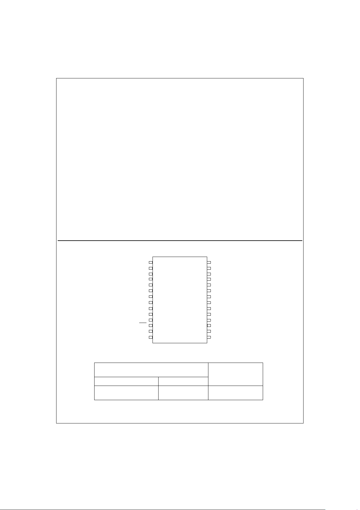
LM9822 3 Channel 42-Bit Color Scanner Analog Front End
Connection Diagram
LM9822
28 pin
SOIC
SCLK
SDI
SEN
D2
D0
V
D
DGND
D4
11
12
13
14
15
16
17
18
19
20
1
2
3
4
5
6
7
8
9
10
23
22
21
24
25
26
27
28
D7
D6
D5
MCLK
V
A
V
A
V
REF-
OS
B
OS
G
CLMP
OS
R
V
REF+
AGND
AGND
VSMP
SDO
V
REFMID
V
BANDGAP
D3
D1
May 1999
LM9822 3 Channel 42-Bit Color Scanner Analog Front End
N
©1999 National Semiconductor Corporation
TRI-STATE® is a registered trademark of National Semiconductor Corporation.
Ordering Information
Notes: 1 - Rail tran spo r t med i a, 2 6 pa rt s per rail, 2 - Tape and reel transport media, 1000 parts per reel
Temperature Range
0°C ≤ T
A
≤ +70°C
NS Package
Number
Order Number Device Marking
LM9822CCWM
1
LM9822CCWMX
2
LM9822CCWM
LM9822CCWM
M28B
M28B
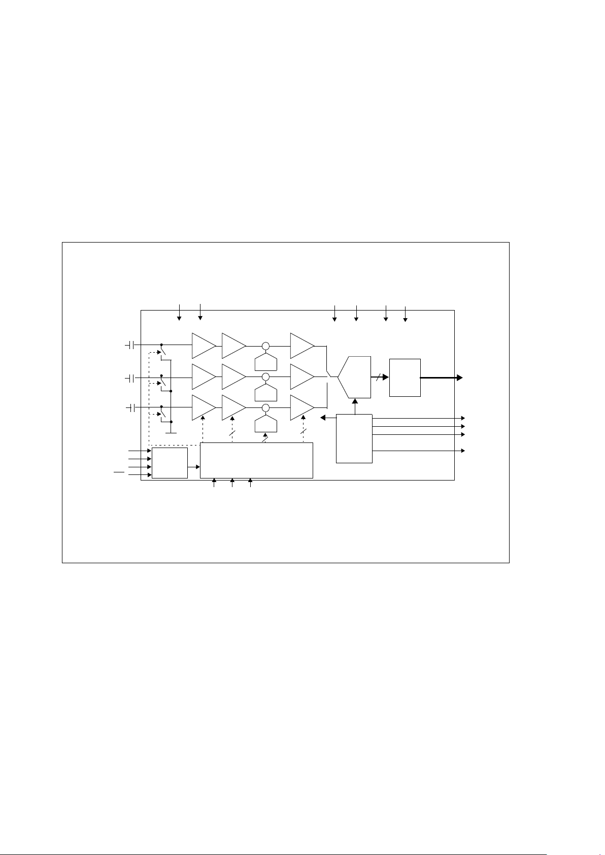
LM9822 Block Diagram
Serial
Interface
Coarse Color
Balance PGAs
DAC
R
Offset
+
+
OS
R
RED OS
from CCD
CDS
OS
G
GREEN OS
from CCD
CDS
OS
B
BLUE OS
from CCD
CDS
x0.93
to x3
DAC
G
Offset
+
+
DAC
B
Offset
+
+
VClamp
x1or x3
Static
Offset
DACs
V
BANDGAP
V
REF+
V
REFMID
V
REF-
Internal
Bandgap
Reference
x1or x3
x1or x3
Gain
Boost
x0.93
to x3
x0.93
to x3
Timing and Control
14
5
6
1
SCLK
SDI
SEN
V
A
V
D
AGND
DGNDVAAGND
MCLK
14 bits
to 8 bit
Bytes
D7 - D0
CLMP VSMP
14-Bit
ADC
SDO
2 www.national.com
3 www.national.com
Electrical Characteristics
The following specifications apply for AGND=DGND=0V, VA=+5.0V
DC
,
V
D
=+3.0 or +5.0VDC, f
MCLK
=12MHz.
Boldface limits apply
for T
A=TJ=TMIN
to T
MAX
; all other limits TA=TJ=25°C. (Notes 7, 8, 12 & 16)
Symbol Parameter Conditions
Typical
(Note 9)
Limits
(Note 10)
Units
(Limits)
CCD/CIS Source Requirements for Full Specified Accuracy an d Dynamic Range
(Note 12)
V
OS PEAK
Sensor’s Maximum Peak Differential
Signal Range
Gain = 0.933
Gain = 3.0
Gain = 9.0
2.1
0.65
0.21
V
V
V
Full Channel Linearity (In un it s of 12 bit LSBs)
(Note 14)
DNL Differential Non-Linearity
+0.9
-0.4
+2
-0.9
LSB(max)
INL Integral Non-Linearity Error (Note 11) ±2.2
+5
-7
LSB(max)
Analog Input Characteristics
OS
R
,
OS
G
,
OS
B
Input Capacitance 5 pF
OS
R
,
OS
G
,
OS
B
Input Leakage Current
Measured with OS = 3.5V
DC
CDS disabled
20
25
µA (max)
CDS enabled 10 nA
Coarse Color Balance PGA Characteristics
Monotonicity
5
bits (min)
G
0
(Minimum PGA Ga in) PGA Setting = 0 0.93
.90
.96
V/V (min)
V/V (m ax)
G
31
(Maximum PGA Gain) PGA Setting = 31 3.0
2.95
3.07
V/V (min)
V/V (m ax)
x3 Boost Gain
x3 Boost Setting On
(Bit 5 of Gain Register is set)
3.0
2.86
3.08
V/V (min)
V/V (m ax)
Gain Error at any gain (Note 13) ±0.3
1.6
% (max)
Static Offset DAC Characteristics (In units of 12 bit LSBs)
Monotonicity
6
bits (min)
Offset DAC LSB size PGA gain = 1 18.9
13
24
LSB (min)
LSB (max)
Offset DAC Adjustment Range PGA gain = 1 ±585
±570
LSB (min)
Positive Supply Voltage (V+=VA=VD)
With Respect to
GND=AGND=DGND
6.5V
Voltage On Any Input or Output Pin -0.3V to V
+
+0.3V
Input Current at any pin (Note 3) ±25mA
Package Input Current (Note 3) ±50mA
Package Dissipation at T
A
= 25°C (Note 4)
ESD Susceptibility (Note 5)
Human Body Model 7000V
Machine Model 450V
Soldering Information
Infrared, 10 seconds (Note 6) 235°C
Storage Temperature -65°C to +150°C
Operating Temperature Range T
MIN
=0°C≤TA≤T
MAX
=+70°C
V
A
Supply Voltage +4.75V to +5.25V
V
D
Supp l y Voltage +3.0V to +5.25V
V
D-VA
≤ 100mV
OS
R
, OSG, OS
B
Input Voltage Range -0.05V to A + 0.05V
SCLK, SDI, SEN
, MCLK, VSMP, CLMP
Input Voltage Range -0.05V to V
D
+ 0.05V
Absolute Maximum Ratings
(Notes 1& 2)
Operating Ratings
(Notes 1& 2)
4 www.national.com
Symbol Parameter Conditions
Typical
(Note 9)
Limits
(Note 10)
Units
(Limits)
Internal Reference Characteristics
V
REFMID
Mid Reference Output Voltage 2.5 V
V
REF+ OUT
Positive Reference Output Voltage 3.5 V
V
REF- OUT
Negative Reference Output Voltage 1.5 V
∆V
REF
Differential Reference Voltage
V
REF+ OUT
- V
REF- OUT
2.0 V
System Characteristics (In units of 12 bit LSBs) (see section 5.1, Internal Offsets)
C
Analog Channel Gain Constant
(ADC Codes/V)
Includes voltage reference
variation, gain setting = 1
2107
1934
2281
LSB (min)
LSB (max)
V
OS1
Pre-Boost Analog Channel Offset Error,
CCD Mode
17.3
-61
+94
LSB (min)
LSB (max)
V
OS1
Pre-Boost Analog Channel Offset Error,
CIS Mode
27
-49
+103
LSB (min)
LSB (max)
V
OS2
Pre-PGA Analog Channel Offset Error -40
-124
+44
LSB (min)
LSB (max)
V
OS3
Post-PGA Analog Channel Offset Error -38
-130
+55
LSB (min)
LSB (max)
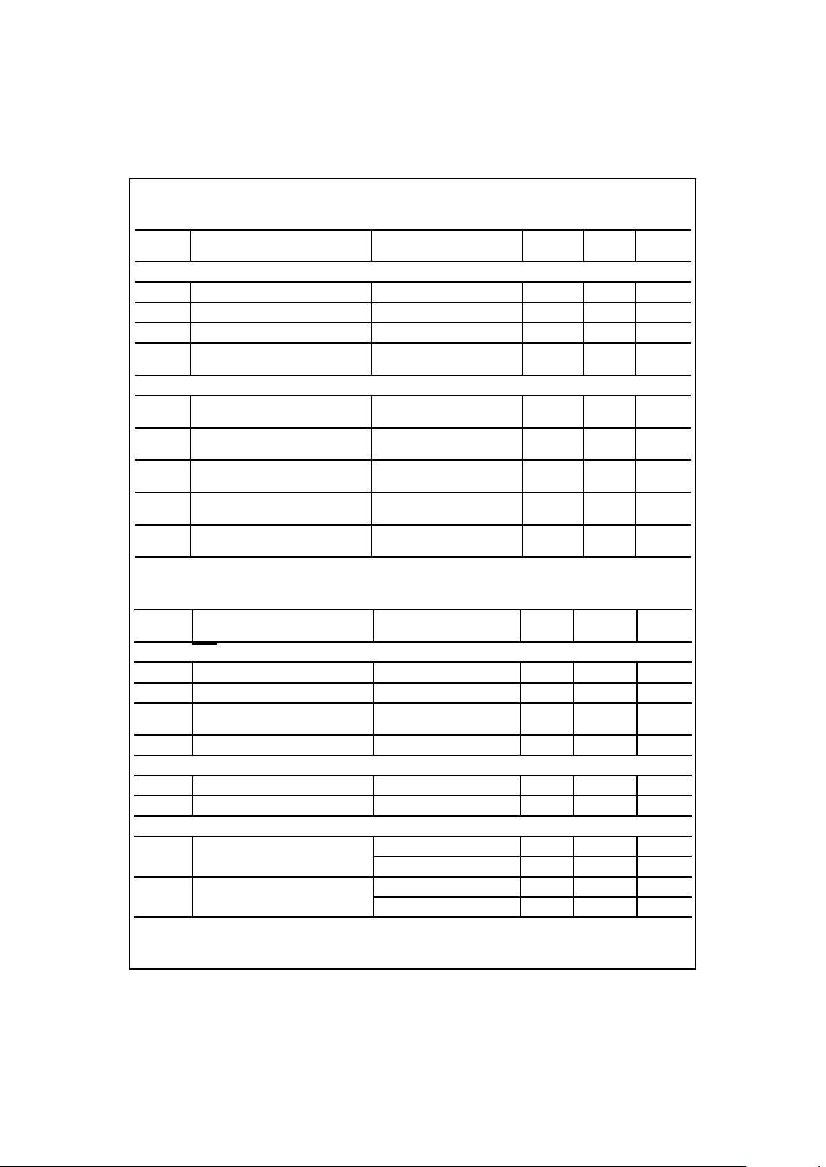
DC and Logic Electrical Characteristics
The following specifications apply for AGND=DGND=0V, VA=+5.0V
DC
,
V
D
=+3.0 or +5.0VDC, f
MCLK
=12MHz.
Boldface limits apply
for T
A=TJ=TMIN
to T
MAX
; all other limits A=TJ=25°C. (Notes 7& 8)
Symbol Parameter Conditions
Typical
(Note 9)
Limits
(Note 10)
Units
(Limits)
SCLK, SDI, SEN,
MCLK, VSMP, CLMP Digital Input Characteristics
V
IN(1)
Logical “1” Input Voltage VA=5.25V
2.0
V (max)
V
IN(0)
Logical “0” Input Voltage VA=4.75V
0.8
V (min)
I
IN
Input Leakage Current
V
IN
=V
A
VIN=DGND
0.1
-0.1
µA(max)
µA(max)
C
IN
Input Capacitance 5 pF
D0-D7 Digital Output Characteristics
V
OUT(1)
Logical “1” Output Voltage I
OUT
=-360µA
0.8*V
D
V (min)
V
OUT(0)
Logical “0” Output Voltage I
OUT
=1.6mA
0.2*V
D
V (max)
Power Supply Characteristics
I
A
Analog Supply Current
Operating 75
108
mA (max)
Power Down 675
900
µA (max)
I
D
Digital Supply Current (Note 15)
Operating 210
475
µA (max)
Power Down 2
25
µA (max)
Electrical Characteristics
(Continued)
The following specifications apply for AGND=DGND=0V, V
A
=+5.0V
DC
,
V
D
=+3.0 or +5.0VDC, f
MCLK
=12MHz.
Boldface limits apply
for T
A=TJ=TMIN
to T
MAX
; all other limits TA=TJ=25°C. (Notes 7, 8, 12 & 16)
5 www.national.com
AC Electrical Characteristics
The following specifications apply for AGND=DGND=0V, VA=+5.0V
DC
,
V
D
=+3.0 or +5.0VDC, f
MCLK
=12MHz, except where noted
otherwise.
Boldface li mit s apply for
A=TJ=TMIN
to T
MAX
; all other limits TA=TJ=25°C. (Notes 7& 8)
Note 1:
Absolute Maximum Ratings indicate limits beyond which damage to the device may occur. Operating Ratings indicate conditions for which the device is functional,
but do not guarantee specific performance limits. For guaranteed specifications and test conditions, see the Electrical Characte ristics. The guaranteed specifications apply
only for the test conditions listed. Some performance characteristics may degrade when the device is not operated under the list ed te st con di tions.
Note 2:
All voltages are measured with respect to GND=AGND=DGND=0V, unless otherwise specified.
Note 3:
When the input voltage (V
IN
) at any pin exceeds the power supplies (VIN<GND or VIN>VA or
V
D
), the current at that pin should be limited to 25mA. The 50m
maximum pac kage input c urre nt ra tin g limits the nu mb er of pin s that can simultaneously safely exceed the power supplies with an input current of 25mA to two.
Note 4:
The maximum power dissipation must be derated at elevated temperatures and is dictated by T
J
max,
Θ
JA
and the ambient temperature, TA. Th e maximum allow-
able power dissipation at any temperature is P
D
= (TJmax - TA) /
Θ
JA
. TJmax = 150°C for this device. The typ ica l t he rmal resi stance (
Θ
JA
) of this p a rt when board mounted
is 69°C /W for the M28 B SOIC package
.
Note 5:
Human body model, 100pF capacitor discharged through a 1.5kΩ resistor. Machine model, 200 pF capacitor discharged through a 0Ω resistor.
Note 6:
See AN450 “Surface Mounting Methods and Their Effect on Product Reliability” or the section titled “Surface Mount” found in any National S e miconductor Linear
Data Book for other methods of so l de r i ng sur f a ce m ount devices.
Note 7:
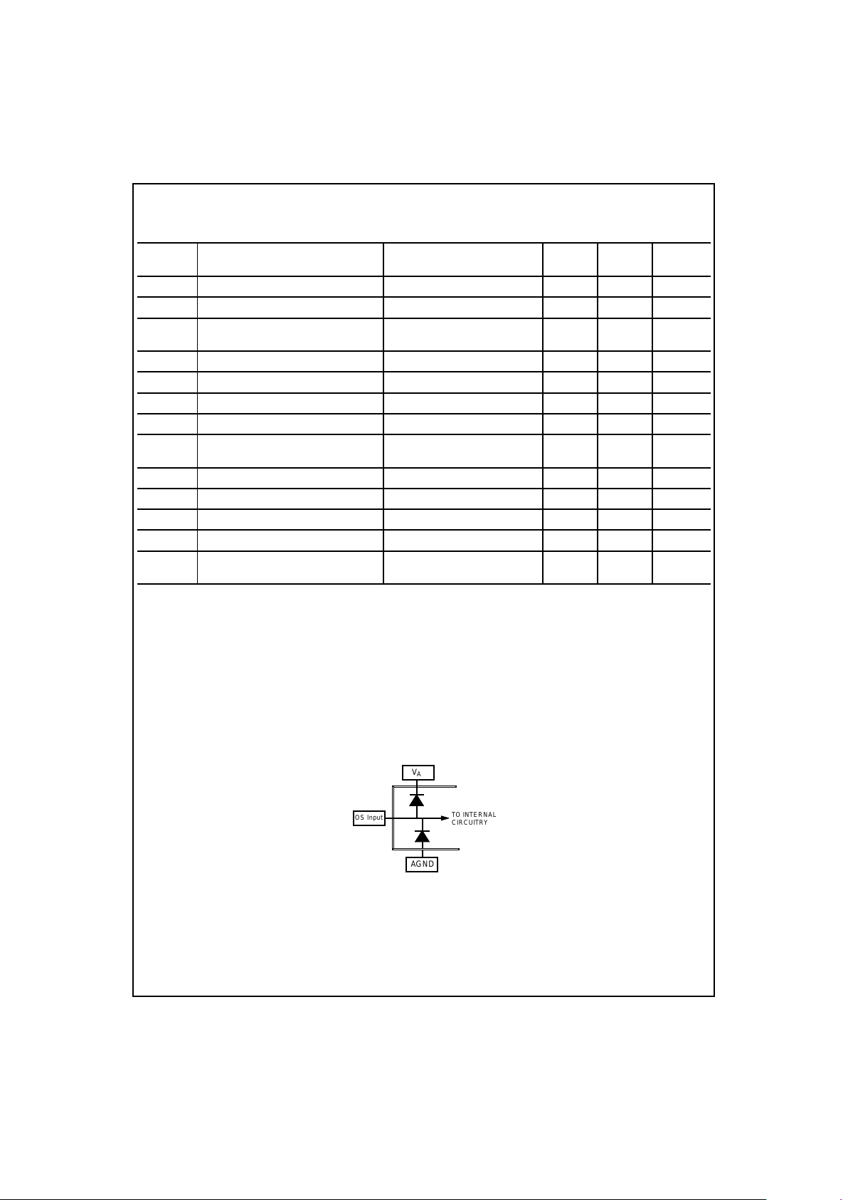
Two diodes clamp the OS analog inputs to
AGND
and
V
A
as shown below. This input protection, in combination with the external clamp capacitor and the output
impedance of the sensor, prevents damage to the LM9822 from transients during power-up.
Note 8:
To guarantee accuracy, it is required that V
A
and VD be connected to clean, low noise power supplies, with separate bypass capacitors at each supply pin. When
both V
A
and VD are operated at 5.0V, they must be powered by the same regulator, with separate power planes or traces and separate bypass capaci to rs at each suppl y pin.
Sym b ol Paramete r Condi tions
Typi cal
(Note 9)
Limits
(Note 10)
Units
(Limits)
f
MCLK
Maximum MCLK frequency
12
MHz (min)
t
MCLK
MCLK period 83 ns (min)
MCLK duty cycle
40
60
%(min)
%(max)
t
SCLK
Serial Clock Period
1
t
MCLK
(min)
t
SEN
Serial Enable high time
3
t
MCLK
(min)
t
SSU
SDI setup time
1
ns (min)
t
SH
SDI hold time
3
ns (min)
t
SDDO
SCLK
edge to new valid data
V
D
= 5.0V
V
D
= 3.3V
8.5
19
20
ns (max)
t
VSU
VSMP setup time
1
ns (min)
t
VH
VSMP hold time
3
ns (min)
t
CSU
CLMP setup time
1
ns (min)
t
CH
CLMP hold time
3
ns (min)
t
DDO
MCLK
edge to new valid data
V
D
= 5.0V
V
D
= 3.3V
16
25
25
ns (max)
ns (max)
OS Input
AGND
V
A
TO INTERN AL
CIRCUITRY
6 www.national.com
Electrical Characteristics
(Continued)
Note 9:
Typicals are at T
J=TA
=25°C, f
MCLK
= 12MHz, and represent most likely parametric norm.
Note 10:
Tested limits are guaranteed to National's AOQL (Average O utgoing Quality Level).
Note 11:
Full channe l integral non-linea rity error is defined a s the d eviation of the analog v alue , expres sed in LSB s, from the straight line tha t best fits th e a ct u al transfer
function of th e AFE.
Note 12:
The sensor’s maximum peak differential signal range is defined as the peak sensor output voltage for a white (full scale) image, with respect to the dark reference
level.
Note 13:
PGA Gain Error is the maximum difference between the measured gain for any PGA code and the ideal gain calculated using:
where .
Note 14:
Full Channel IN L and DN L are te st e d w i th C DS disab le d, negative sign al pola rity , DOE = 0, and a si ngle OS inpu t with a gain register se ttin g of 1 (0 00 0 0 1b) and
an offset re gi st er s et ti ng o f 0 (0 00 000b).
Note 15:
The digital supply current (ID) does not include the load, data and switching frequency dependent current required to drive the digital output bus on pins (D7 - D0).
The curre nt requir ed to switch t he digita l d ata bus can be calc ulate d f rom : Isw = 2*N d*Psw* CL*V
D/tMCLK
where N d is total num ber of da ta pins, Psw is the pr obability of
each data bit switching, CL is the capacitive loading on each d ata pin, V
D
is the digital supply voltage and t
MCLK
is the period of the MCLK input. For most applications, Nd
is 8, Psw is ≈ 0.5, and V
D
is 5V, and the switching current can be calculated from: Isw = 40*CL/tMCLK. (With D at 3.3V, the equation bec omes : Isw = 2 6.4*CL/t
MCLK
.) For
example, if the capacitive load on each digital output pin (D7 - D0) is 20pF and the period of t
MCLK
is 1/12MHz or 83ns, then the digital switching current would be 9.6mA.
The calculated digital switching current will be drawn through the V
D
pin and should be c on s idere d a s part of th e total po wer bu d ge t for the LM9822.
Note 16:
All specifications quoted in LSBs are based on 12 bit resolution.
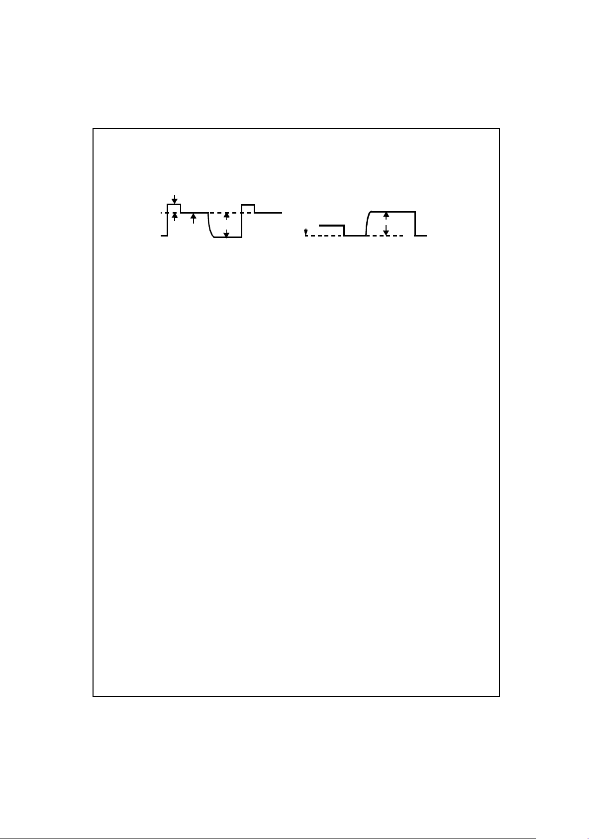
V
WHITE
V
REF
V
RFT
CCD Output Signal
CIS Output Signal
V
WHIT
Black Level
Gain
PGA
V
V
--- -
G0X
PGA code
32
-------------- -------------- -+=XG
31G0
–
()
32
31
----- -=
7 www.national.com
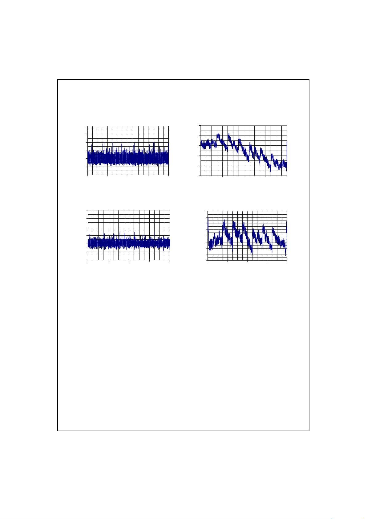
Typical Performance Characteristics
Full Channel DNL and INL
(Divide by 2, Monochrome Mode, 6 MHz Pixel Rate)
Note:
The LM9822 provides 14-bit data for high resolution imaging applications. The typical full channel device performance is shown
in the above graphs. In many applications, particularly those where high speed is important, or where lower cost CCD and CIS sensors
are used, the signal source is only accurate to 12 bits. In these applications, only 12-bit of data may be used. 12-bit DNL and INL pl ots
have also been provided to illustrate the performance of the LM9822 in these applications.
Typical 12 Bit DNL
-1
-0.5
0
0.5
1
1.5
2
0 1024 2048 3072 4096
Output Code
LSB
Typical 12 Bit INL
-2.5
-2
-1.5
-1
-0.5
0
0.5
1
1.5
0 1024 2048 3072 4096
Output Code
LSB
Typical 14 Bit DNL
-1
-0.5
0
0.5
1
1.5
2
0 4096 8192 12288 16384
Output Code
LSB
Typical 14 Bit INL
-15
-10
-5
0
5
10
0 4096 8192 12288 16384
Output Code
LSB
 Loading...