

N
LM9812 30-Bit Color Linear CCD Sensor Processor
LM9812 30-Bit Color Linear CCD Sensor Processor
December 1997
General Description
The LM9812 is a high performance integrated signal processor/digitizer for color linear CCD image scanners. The LM9812
performs all the si gnal processing ( correlated double sa mpling,
pixel rate offset and shading correc tion, color balance control,
and 10-bit analog-to- digital conversion) necessary to maximize
the performance of a wide range of linear CCD sensors.
The LM9812 can be digitally programme d to work with a wi de
variety of CCDs from different manufacture rs, including both 3
output RGB and 2 output GRGB CCDs. An internal Configuration Register sets CCD and sampling timing to maximize performance, simplifying the design and manufacturing processes. For
complementary voltage reference see the LM4041-ADJ.
Applications
•
Color Flatbed Document Scanners
•
Color Sheetfed Scanners
•
Multifunction Imaging Products
•
Digital Copiers
•
General Purpose Linear CCD Imaging
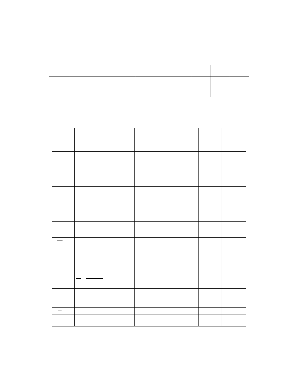
Connection Diagrams
OSROSGOSBV
TR2
8
TR1
9
RS
10
ø2
11
ø1
SYNC
CS
RD
WR
MCLK
OCLK
GCLK
12
13
14
15
16
17
18
19
20
LM9812CCV
21 22 23 24 25 26 27 28 29 30 31 32 33
CD9
CD8
CD7
CD6
RUN/STOP
Features
•
6 million pixels/s conversion rate (2MHz/channel x 3)
•
Pixel rate shading (gain) correction for individual pixels
eliminates errors from PRNU, illumination, etc.
•
Digitally programmed color balance controls
•
Pixel rate offset correction for highest quality in dark regions
•
Correlated Double Sampling for lowest noise
•
Reference and signal sampling points digitally controlled in
20ns increments
•
2x and 4x analog fast preview/low resolution modes
•
Digital control of CCD integration time
•
Generates all necessary CCD clock signals
•
Compatible with a wide range of color linear CCDs and
Contact Image Sensors (CIS)
•
TTL/CMOS input/output compatible
Key Specifications
•
Output Data Resolution 10 Bits
•
Pixel Conversion Rate (total) 6MHz
•
Supply Voltage +5V±5%
•
Supply Voltage (Digital I/O) +3.3V±10% or +5V±5%
•
Power Dissipation (typical) 390mW
REF IN
A
AGND
V
V
1234567
D
V
CD5
DGND
REF MID OUTVREF MID INVREF HI OUT
REF HI IN
V
52 51 50 49 48 47
CD4
CD3
CD2
CD1
REF LO OUTVREF LO IN
V
CD0
TEST
EOC
46
45
44
43
42
41
40
39
38
37
36
35
34
D9
D8
D7
D6
D5
V
DI/O
D4
DGND
I/O
D3
D2
D1
D0
RD PIXEL
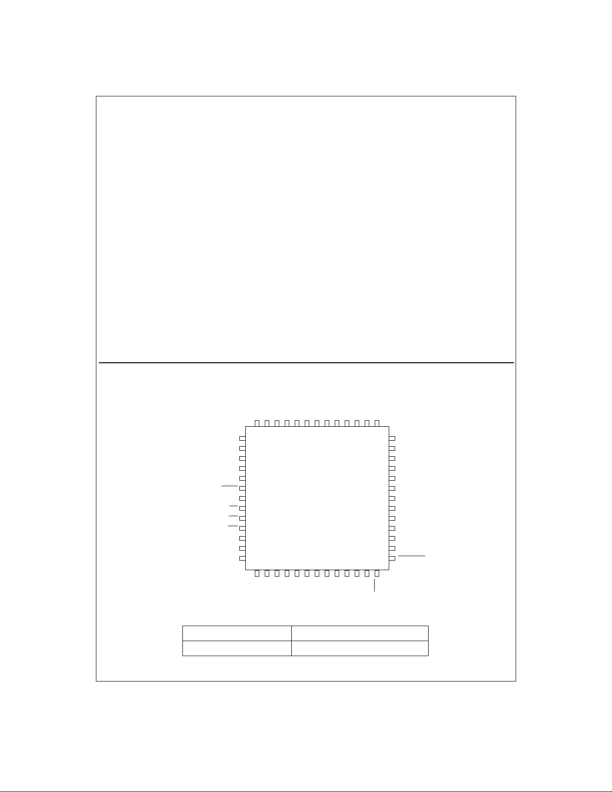
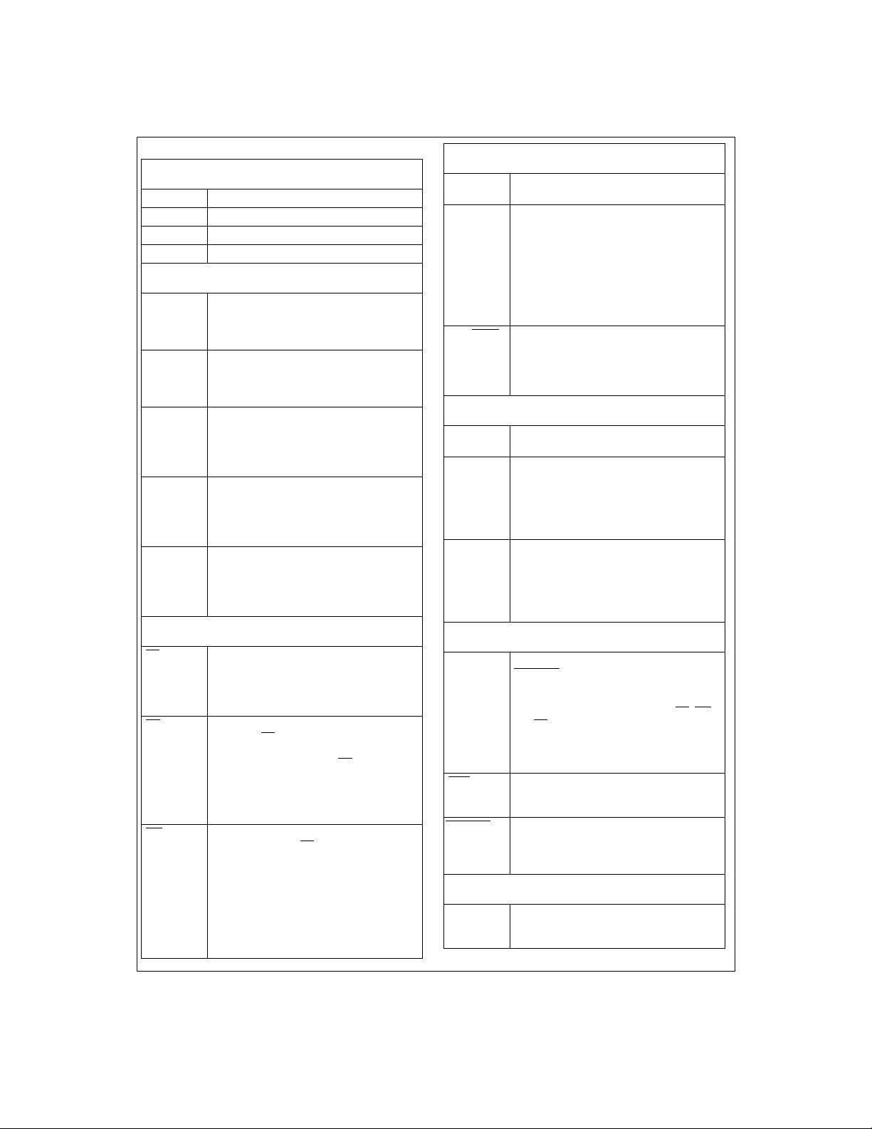
Ordering Information
Commercial (0°C ≤ TA ≤ +70°C) Package
LM9812CCV V52A 52 Pin Plastic Leaded Chip Carrier
TRI-STATE® is a registered trademark of National Semiconductor Corporation.
©1997 National Semiconductor Corporation
1
http://www.national.com
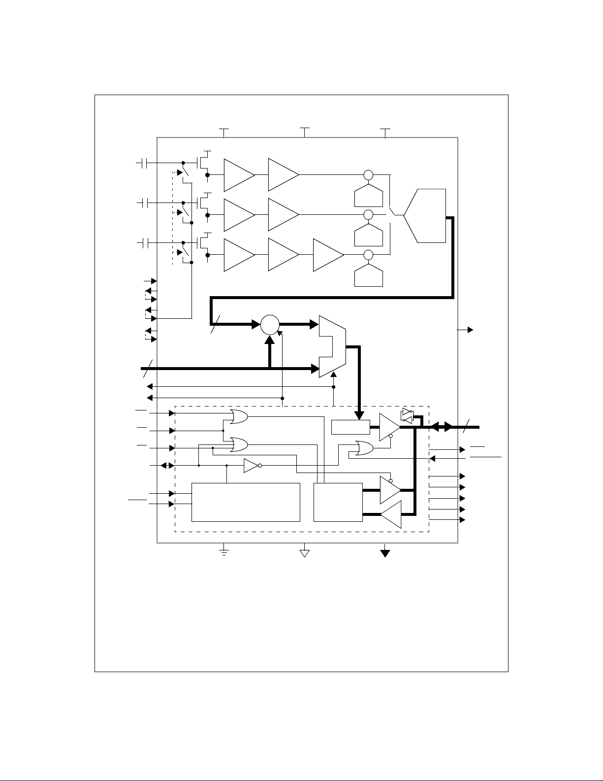
Block Diagram
RED OS
from Sensor
GREEN OS
from Sensor
BLUE OS
from Sensor
V
REF IN
V
REF LO OUT
V
REF LO IN
V
REF MID OUT
V
REF MID IN
V
REF HI OUT
V
REF HI IN
Gain/Offset
Coefficients
CD0-CD9
GCLK
SYNC
MCLK
RUN/STOP
OCLK
WR
CS
RD
OS
OS
OS
10
R
G
B
CLAMP
V
A
Coarse Color
Balance PGAs
CDS
CDS
CDS
x1-x3
x1-x3
x1-x3
Pixel-Rate Offset Subtractor
+
10 bits
+
-
Control
Logic
V
D
Blue Gain
x1or x3
Boost
Pixel-Rate
Shading Multiplier
Pixel Data
Latch
Configuration
Register
Static
Offset
DACs
+
²
+
Offset
DAC
+
²
+
Offset
DAC
+
²
+
Offset
DAC
V
DI/O
R
10-Bit,
6MHz
ADC
G
B
TEST
Pixel Data Output/
Control Data I/O
10
D0-D9
EOC
RD PIXEL
ø1
ø2
RS
TR1
TR2
AGND
DGND
2
DGND
I/O
http://www.national.com
Absolute Maximum Ratings
Positive Supply Voltage (V+=VA=VD=V
With Respect to GND=AGND=DGND=DGND
Voltage On Any Input or Output Pin 0.3V to V
DI/O
(Notes 1 & 2)
)
I/O
+
+0.3V
Input Current at any pin (Note 3) ±25mA
Package Input Current (Note 3) ±50mA
Package Dissipation at T
ESD Susceptibility (Note 5)
= 25°C (Note 4)
A
Human Body Model 2000V
Soldering Information
Infrared, 10 seconds (Note 6) 300°C
Storage Temperature -65°C to +150°
Operating Ratings
Operating Temperature Range T
6.5V
LM9812CCV 0°C≤T
V
Supply Voltage +4.75V to +5.25V
A
V
Supply Voltage +4.75V to +5.25V
D
V
Supply Voltage +3.0V to +5.25V
DI/O
|V
|
A-VD
V
A-VDI/O
OS
, OSG, OSB, V
R
Input Voltage Range -0.05V to V
CD0-CD9, D0-D9, MCLK, SYNC,
RUN/STOP
REF IN
, CS, RD, WR, RD PIXEL
(Notes 1 & 2)
Input Voltage Range -0.05V to V
≤
MIN
≤
< -100mV
A
DI/O
Electrical Characteristics
The following specifications apply for AGND=DGND=DGND
f
=24MHz, Rs=25Ω. Boldface limits apply for T
MCLK
=0V, VA=VD=+5.0V
I/O
A=TJ=TMIN
to T
; all other limits TA=TJ=25°C. (Notes 7, 8, & 12)
MAX
CCD/CIS Source Requirements for Full Specified Accuracy and Dynamic Range (Note 12)
Color Balance PGA gain = 0.933
V
OS PEAK
Sensor’s Maximum Peak Differential
Signal Range
Color Balance PGA gain = 3.0
Color Balance PGA gain = 9.0
(Blue Channel, BOOST on)
Sensor’s Maximum Correctable Range
of Pixel-to-Pixel V
Variation/Color
WHITE
Range 0
Range 1
Range 2
Coarse Color Balance PGA Characteristics
Monotonicity 5 bits (min)
G
(Minimum PGA Gain) PGA Setting = 0 0.93
0
G
(Maximum PGA Gain) PGA Setting = 31 3.00
31
G
BLUE BOOST
Blue PGA Boost Setting = x3 3.00
Gain Error at any gain (Note 14) ±1.0 ±4.0
Static Offset DAC Characteristics
Monotonicity 6 bits (min)
Offset DAC LSB size In units of ADC LSBs 4.2
Offset DAC Adjustment Range In units of ADC LSBs ±130 ±118 LSB (min)
ADC Characteristics
Resolution with No Missing Codes 10 Bits (min)
ILE Integral Linearity Error (Note 11) ±0.4 ±1.5 LSB (max)
DNL Differential Non-Linearity
System Characteristics
C Analog Channel Gain Constant 2.00
, V
=+5.0 or +3.3VDC, V
DC
DI/O
-0.14
+0.32
REF IN
1.0
0.33
0.11
67 (1:3)
50 (1:2)
33 (1:1.5)
0.90
0.97
2.85
3.20
2.72
3.27
1.3
7.2
-0.5
+1.0
1.83
2.17
= +2.0VDC,
≤
T
T
A
MAX
≤
+70°C
A
100mV
+ 0.05V
+ 0.05V
V (min)
V (min)
V (min)
%
%
%
V/V (max)
V/V (min)
V/V (max)
V/V (min)
V/V (max)
V/V (min)
% (min)
% (max)
LSB (min)
LSB (max)
LSB (min)
LSB (max)
(min)
(max)
3
http://www.national.com
Electrical Characteristics
The following specifications apply for AGND=DGND=DGND
f
=24MHz, Rs=25Ω.
MCLK
V
V
V
Pre-PGA Analog Channel Offset Error
OS1
CCD Mode
Pre-PGA Analog Channel Offset Error
OS1
CIS Mode
Post-PGA Analog Channel Offset Error In units of ADC LSBs -5
OS2
Boldface limits apply for T
(Continued)
V
V
=0V,
=
I/O
A=TJ=TMIN
=
A
D
to T
; all other limits TA=TJ=25°C. (Notes 7, 8, & 12)
MAX
In units of ADC LSBs +5
In units of ADC LSBs +32
Reference and Analog Input Characteristics
OS
, OSG, OSB Input Capacitance 5 pF
R
OS
, OSG, OSB Input Leakage Current Measured with OS = 2.5V
R
V
Input Leakage Current Measured with V
REF IN
REF IN
DC and Logic Electrical Characteristics
V
The following specifications apply for AGND=DGND=DGND
f
=24MHz, Rs=25Ω.
MCLK
Boldface limits apply for T
I/O
A=TJ=TMIN
Symbol Parameter Conditions
D0-D9, CD0-CD9, MCLK, RUN/STOP
V
V
C
D0-D9, EOC
V
OUT(1)
V
OUT(0)
I
OUT
Logical “1” Input Voltage
IN(1)
Logical “0” Input Voltage
IN(0)
I
Input Leakage Current
IN
Input Capacitance 5 pF
IN
, GCLK, OCLK, SYNC Digital Output Characteristics
Logical “1” Output Voltage
Logical “0” Output Voltage
TRI-STATE® Output Current
(D0-D9 only)
, SYNC, CS, RD, WR, RD PIXEL Digital Input Characteristics
V
DI/O
V
DI/O
V
DI/O
V
DI/O
V
=V
IN
VIN=DGND
V
DI/O
V
DI/O
V
DI/O
V
DI/O
V
DI/O
V
DI/O
V
OUT
V
OUT
Ø1, Ø2, RS, TR1, TR2 Digital Output Characteristics
V
=4.75V, I
V
V
OUT(1)
OUT(0)
Logical “1” Output Voltage
Logical “0” Output Voltage VD=5.25V, I
D
V
=4.75V, I
D
Power Supply Characteristics
Analog Supply Current
I
A
I
Digital Supply Current
D
Operating
Standby
Operating
Standby
V
=0V,
=
=
A
D
to T
; all other limits TA=TJ=25°C. (Notes 7 & 8)
MAX
=5.25V
=3.6V
=4.75V
=3.0V
D
=4.75V, I
OUT
=4.75V, I
OUT
=3.0V, I
=3.0V, I
=5.25V, I
=3.6V, I
OUT
OUT
OUT
OUT
=-360µA
=-10µA
=1.6mA
=DGND
=V
D
=-360µA
OUT
=-10µA
OUT
=1.6mA
OUT
+5.0
V
= 2.0V
+5.0
V
=-360µA
=-10µA
=1.6mA
, V
=+5.0 or +3.3VDC, V
DC
DI/O
DC
DC
, V
=+5.0 or +3.3VDC, V
DC
DI/O
2
4
Typical
(Note 9)
0.1
-0.1
0.1
-0.1
60
7
4.7
0.1
REF IN
-40
+40
-65
+135
-40
+30
20
20
REF IN
Limits
(Note 10)
2.0
2.0
0.8
0.7
2.4
4.4
2.1
2.5
0.4
0.4
2.4
4.4
0.4
85
10
10
1.0
= +2.0VDC,
LSB (min)
LSB (max)
LSB (min)
LSB (max)
LSB (min)
LSB (max)
nA (max)
nA (max)
= +2.0VDC,
Units
(Limits)
V (min)
V (min)
V (max)
V (max)
µA
µA
V (min)
V (min)
V (min)
V (min)
V (max)
V (max)
µA
µA
V (min)
V (min)
V (max)
mA (max)
mA (max)
mA (max)
mA (max)
4
http://www.national.com
DC and Logic Electrical Characteristics
The following specifications apply for AGND=DGND=DGND
f
=24MHz, Rs=25Ω.
MCLK
Boldface limits apply for T
A=TJ=TMIN
I/O
(Continued)
V
V
=0V,
to T
+5.0
=
=
A
D
; all other limits TA=TJ=25°C. (Notes 7 & 8)
MAX
Symbol Parameter Conditions
I
DI/O
Digital I/O Supply Current
Operating, V
Standby, V
Operating, V
Standby, V
DI/O
DI/O
DI/O
= 5.0V
DI/O
= 3.3V
=5.0V
=3.3V
AC Electrical Characteristics, MCLK Independent
V
V
The following specifications apply for AGND=DGND=DGND
, tr=tf=5ns
=1/f
t
MCLK
MCLK
Boldface limits apply for T
, R
=25¾, CL (databus loading) = 50pF/pin.
s
A=TJ=TMIN
to T
; all other limits TA=TJ=25°C. (Notes 7 & 8)
MAX
I/O
=0V,
Symbol Parameter Conditions
f
MCLK
Maximum MCLK Frequency
Minimum MCLK Frequency
MCLK Duty Cycle
t
SETUP (OUT)
t
HOLD (OUT)
t
SETUP (IN)
t
HOLD (IN)
t
GCLK-EOC
Coefficient Data valid before latching
edge of OCLK or GCLK
Coefficient Data held after latching
edge of OCLK or GCLK
Coefficient Data Valid before latching
edge of OCLK or GCLK
Coefficient Data held after latching
edge of OCLK or GCLK
Rising edge of GLCK to falling edge
of EOC
(GCLK as output)
GCLK and OCLK as
outputs
GCLK and OCLK as
outputs
GCLK and OCLK as
inputs
GCLK and OCLK as
inputs
Rising edge of GLCK to falling edge
t
GCLK-OCLK
t
EOC-OCLK
t
OCLK-GCLK
of OCLK (GCLK and OCLK as
outputs)
Rising edge of EOC to rising edge of
OLCK (OCLK as output)
Rising edge of OLCK to falling edge
of GLCK (GCLK and OCLK as
2 bus / 2 clock mode 1 ns
2 clock mode 1 ns
2 clock mode 3 ns
outputs)
t
EOC-GCLK
t
DACC
t
D1H, D0H
t
CS SETUP
t
CS HOLD
t
WR SETUP
Rising edge of EOC to falling edge of
GLCK (GCLK as output)
RD or RD_PIXEL low to D0-D9 data
valid
RD or RD_PIXEL high to D0 - D 9 da ta
tri-state
CS setup of RD or WR
CS hold after RD or WR
D0-D9 data valid before rising edge
of WR
(setup time)
2 bus mode 2 ns
V
=
=
A
D
V
DI/O
, V
=+5.0 or +3.3VDC, V
DC
DI/O
=+5.0
V
DC
Typical
(Note 9)
12
-10
0
0
,
V
Typical
(Note 9)
12
5
2
0.3
REF IN
= +2.0VDC, f
Limits
(Note 10)
24
4
40
60
20
0
5
5
REF IN
Limits
(Note 10)
30
20
10
3
MCLK
= +2.0VDC,
Units
(Limits)
mA (max)
mA (max)
mA (max)
mA (max)
=24MHz
Units
(Limits)
MHz (min)
MHz (max)
% (min)
% (max)
ns (min)
ns (min)
ns (min)
ns (min)
,
2ns
15
13
41
20
0
0
5
ns (max)
ns (max)
ns (min)
ns (min)
ns (min)
5
http://www.national.com
AC Electrical Characteristics, MCLK Independent
The following specifications apply for AGND=DGND=DGND
, tr=tf=5ns
=1/f
t
MCLK
MCLK
Boldface limits apply for T
, R
=25¾, CL (databus loading) = 50pF/pin.
s
A=TJ=TMIN
to T
; all other limits TA=TJ=25°C. (Notes 7 & 8)
MAX
I/O
=0V,
Symbol Parameter Conditions
t
WR HOLD
D0-D9 data valid after rising edge of
WR
(hold time)
V
=
A
=+5.0
V
V
=
D
DI/O
AC Electrical Characteristics, MCLK Dependent
The following specifications apply for AGND=DGND=DGND
=1/f
t
MCLK
MCLK
labeled C.R.
, tr=tf=5ns
Boldface limits apply for T
, R
=25Ω, CL (databus loading) = 50pF/pin. Refer to Table 2: Configuration Register Parameters for limits
s
A=TJ=TMIN
to T
=0V,
I/O
; all other limits TA=TJ=25°C. (Notes 7 & 8)
MAX
Symbol Parameter Conditions
t
R/S START
t
START
t
SYNC END
Rising edge of RUN/STOP to Rising
edge of SYNC
Rising edge of SYNC to rising edge
of TR1
Falling edge of SYNC to last rising
edge of EOC
SYNC OUT mode
SYNC IN mode
SYNC IN mode
SYNC OUT mode
SYNC IN mode
SYNC OUT mode
SYNC IN mode
t
SYNC LOW
t
TR1 WIDTH
t
TR2 WIDTH
t
GUARD
t
RS WIDTH
t
CLAMP ON
t
CLAMP OFF
t
t
RS
t
HOLD REF
t
HOLD SIG
t
OCLK LOW
t
OCLK HIGH
t
GCLK LOW
t
GCLK HIGH
SYNC low time
,
TR1, TR2 Transfer Pulse Width
TR1, TR2 Transfer Pulse Guardband
Reset Pulse Width
Start of Optical Black clamping
period
End of Optical Black clamping period
Ø1, Ø2 clock period
Ø
RS pulse position from Ø1 edge
Reference hold (sample) position
from RS edge
Signal hold (sample) position from
RS edge
OCLK low time (OCLK as Output)
OCLK high time (OCLK as Output)
GCLK low time (GCLK as Output)
GCLK high time (GCLK as Output)
SYNC OUT mode
Standard Mode
Even/Odd Mode
2 bus mode
1bus mode
2 bus mode
1 bus mode
2 bus mode
1 bus mode
2 bus mode
1 bus mode
V
=
A
=+5.0
V
V
=
D
DI/O
(Continued)
V
DC
Typical
(Note 9)
V
DC
Typical
(Note 9)
t
1+
GUARDBAND
t
13+
GUARDBAND
t
GUARDBAND
8
0
,
,
V
REF IN
V
REF IN
= +2.0VDC, f
Limits
(Note 10)
0
= +2.0VDC, f
Limits
(Note 10)
16
t
GUARDBAND
14+
t
GUARDBAND
t
GUARDBAND
9
0
8
# of EOL
PIxels - 4
C.R.
C.R.
C.R.
C.R.
C.R.
12
24
C.R.
C.R.
C.R.
2*t
MCLK
1*t
MCLK
2*t
MCLK
3*t
MCLK
2*t
MCLK
1*t
MCLK
2*t
MCLK
3*t
MCLK
MCLK
MCLK
MCLKs (max)
MCLKs (min)
MCLKs (max)
MCLKs (max)
MCLKs (max)
MCLKs (min)
Pixel periods
=24MHz
Units
(Limits)
ns (min)
=24MHz
Units
(Limits)
MCLKs
MCLKs
MCLKs
MCLKs
MCLKs
MCLKs
MCLKs
MCLKs
MCLKs
MCLKs
MCLKs
ns
ns
ns
ns
,
,
6
http://www.national.com
AC Electrical Characteristics, MCLK Dependent
V
V
=0V,
The following specifications apply for AGND=DGND=DGND
t
MCLK
labeled C.R.
, tr=tf=5ns
=1/f
MCLK
Boldface limits apply for T
, R
=25Ω, CL (databus loading) = 50pF/pin. Refer to Table 2: Configuration Register Parameters for limits
s
A=TJ=TMIN
I/O
to T
; all other limits TA=TJ=25°C. (Notes 7 & 8)
MAX
Symbol Parameter Conditions
t
EOC LOW
t
EOC HIGH
t
DATA VALID
EOC low time
EOC high time
D0-D9 data valid from falling
Read Phase = 0°)
Phase = 180°)
edge of EOC
or rising
(Data Read
(Data
=
A
D
V
=
(Continued)
=+5.0
DI/O
,
V
DC
Typical
(Note 9)
V
REF IN
= +2.0VDC, f
Limits
(Note 10)
2*t
MCLK
2*t
MCLK
4*t
-20ns
MCLK
MCLK
=24MHz
Units
(Limits)
ns
ns
ns (min)
,
OCLK rising edge to EOC falling edge
t
t
OCLK-EOC 1
(OCLK IN)
(Gain Coefficient Write Phase = 0°),
OCLK falling edge to EOC falling edge
(Gain Coefficient Write Phase = 180°)
1 bus mode w/ext OCLK
MCLK
4*t
+ 40ns
MCLK
ns (min)
ns (max)
OCLK rising edge to EOC rising edge
t
OCLK-EOC 2
(OCLK IN)
(Gain Coefficient Write Phase = 0°),
OCLK falling edge to EOC rising edge
(Gain Coefficient Write Phase = 180°)
2 bus mode w/ext OCLK
3*t
40ns
MCLK
ns (min)
ns (max)
GCLK rising edge to EOC falling edge
t
GCLK-EOC
(GCLK IN)
Note 1: Absolute Maximum Ratings indicate limits beyond which damage to the device may occur. Operating Ratings indicate conditions for which the device is functional,
but do not guaran te e specific performance limits. For guarante ed specifications and test conditio ns, s ee the Electrical Characteristics. Th e guaranteed spec if ic at ions apply
only for the test conditio ns lis t ed. Some performance c haracteristics may degrade w hen the device is not operated under the listed test conditions.
Note 2: All voltages are measured with respect to GND=AGND=DGND=DGND
Note 3: When the input voltage (V
imum package input cu rrent rating limits the numb er of pins that can simultaneously safely exceed the power supplies with an input current of 25mA to two.
Note 4: The maximum powe r dissipa tion must be de rated at elevated temp eratur es and is dicta ted by T
able power dissipatio n at any temperature is P
is 52°C/W for the V52A PLCC package
Note 5: Human body model, 100pF capacitor discharged through a 1.5kΩ resistor.
Note 6: See AN450 “Surface Mounting Methods and Their Effect on Product Reliability” or the section ti tl ed “Surface Mount” found in any post 1986 National Semiconduc-
tor Linear Data Book for other methods of solder ing surface mount devices.
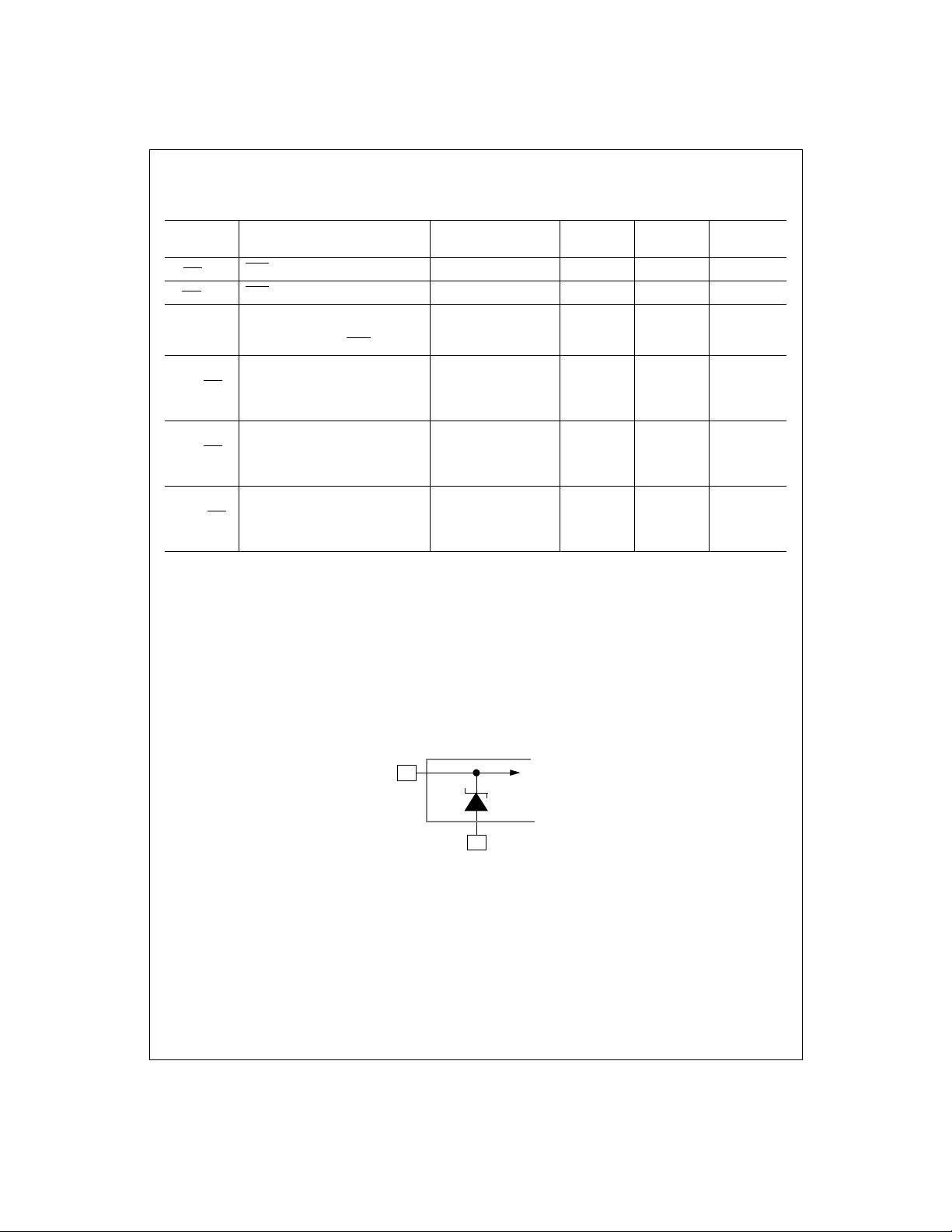
Note 7: A Zener diode c lamps the OS an alog inputs to AGND as shown below. This input prote ction, in combin ation with the exter nal clamp capaci tor and the outpu t
impedance of the se ns or, prevents dam age to the LM9812 fro m tran s ients during power-up.
(Gain Coefficient Write Phase = 0°),
GCLK falling edge to EOC falling edge
(Gain Coefficient Write Phase = 180°)
) at any pin exceeds the power supplies (VIN<GND or VIN>VA or VD), the current at that pin should be limited to 25mA. The 50mA max-
IN
= (TJmax - TA) / ΘJA. TJmax = 150°C for this device. The typical thermal resistance (ΘJA) of this part when board mounted
D
.
w/ext GCLK
=0V, unless otherwise specified.
I/O
max, ΘJA and the ambie nt temperature, TA. The maximum allow-
J
3*t
40ns
MCLK
ns (min)
ns (max)
OS Input
AGND
Note 8: To guarantee accuracy, it is required that V
Note 9: Typicals are at T
Note 10: Tested limits are guaranteed to Na t ional's AOQL (Average Outgoing Qualit y Level).
Note 11: Integral linearity error is defined as the deviation of the analog value, expressed in LSBs, from the straight line that best fits the actual transfer function of the ADC.
Note 12: V
a white (full scale) image with respect to the reference level, V
correctable range o f pixel-to-pixel V
is defined as the CCD OS voltage for the reference period f ollowing the reset feedthrough pulse. V
REF
J=TA
=25°C, f
MCLK
WHITE
and VD be connected together to the same power supply w it h s eparate bypass capacito rs at eac h supply pin.
A
= 24MHz, and represent most likely parametric norm.
is defined as the peak positive deviation above V
. V
REF
variation is defi ned as the maxim um variation in V
RFT
7
To Internal
Circuitry
is defined as the peak CCD pixel output voltage for
WHITE
of the reset feedthrough pulse. The maximum
(due to PRNU, light source intensity variation, optics, etc.) that the
WHITE
REF
http://www.national.com
LM9812 can correc t for using its internal PGA.
CCD Output Signal
V
RFT
V
Note 13: Reference voltages below 1.80V may decreas e SNR. Reference voltages above 2.20V may cause linearity (headroom) errors inside the LM9812. The
LM4041DIM3-A D J (SOT-23 package) or the LM4041DIZ-ADJ (TO-92 package) bandgap voltage references are recommended for this application.
Note 14: PGA Gain Error is the maximum difference between the measured gain for any PGA code and the ideal gain calculated by using the formula
V
--- -
Gain
PGA
V
PGA code
G0X
---------------- ---------- -+=XG
where .
32
32
–()
------=
31G0
31
V
REF
WHITE
8
http://www.national.com
Pin Descriptions
Sensor Driver Signals
ø1 Digital Output. Clock signal, phase 1.
ø2 Digital Output. Clock signal, phase 2.
RS Digital Output. Reset pulse.
TR1, TR2 Digital Output. Transfer pulses.
Analog I/O
OSR, OSG,
OS
,
B
V
REF IN
V
REF LO OUT,
V
REF LO IN
V
REF MID OUT,
V
REF MID IN
V
REF HI OUT,
V
REF HI IN
Analog Inputs. These inputs (for Red, Green,
and Blue) should be tied to the sensor’s OS
(Output Signal) through DC blocking capacitors.
Analog Input. This is the system reference voltage input and should be connected to a 2.0V
voltage source and bypassed to AGND wi th a
0.05µF monolithic capacit or.
Analog Output/Input. V
equal to 0.49V
=2V) developed by the LM9812. It should be
IN
tied to V
REF LO IN
a 0.05µF monolithic capacitor.
Analog Output/Input. V
equal to 0.49V
oped by the LM9812. It should be tied to V
and bypassed to AGND with a 0.05µF
MID IN
monolithic capacitor.
Analog Output/Input. V
equal to 0.49V
=2V) developed by the LM9812. It should be
IN
tied to V
REF HI IN
0.05µF monolithic capacit or.
REF LO OUT
- V
A
REF IN
and bypassed to AGND with
REF MID OUT
(2.45V for V
A
REF HI OUT
+ V
A
REF IN
and bypassed to AGND with a
is a voltage
/2 (1.45V for V
is a voltage
=2V) devel-
REF IN
is a voltage
/2 (3.45V for V
REF
REF
Configuration Register I/O
CS Digital Input. This is the Chip Select signal for
RD
WR
reading or writing to the Configuration Register
through the D0-D9 databus. This input must be
low in order to enable writing to or reading from
the Configuration Register.
Digital Input. A low signal on this input, when
SYNC and CS
the currently addressed Configuration Register on the D0-D9 databus. A RD
resets the internal address latching state
machine. NOTE: If this pin is taken low when
CS is high, the D0-D9 databus will come out of
tri-state and drive random data onto the bus.
Digital Input. This input, when simultaneously
asserted along with CS
the D0-D9 databus to the LM9812. If this is the
first write in the cycle, this data is the address
to be read or written to. If this is the second
write in the cycle, this data is the data to be
written to the Configuration Register at the currently latched address. Writing to the Configuration Register is independent of the state of
SYNC.
are also low, pl aces the data in
cycle also
, transfers the data on
REF
General Digital I/O
MCLK Digital Input. This is the 24MHz (typical) master
SYNC Digital Input (SYNC_IN mode) /
RUN/STOP
system clock.
Digital Output (SYNC_OUT mode).
In the SYNC_IN mode, a low-to-high transition
on this input begins a line scan operation. The
line scan operation terminates when SYNC is
taken low. In the SYNC_OUT mode, the rising
edge of this output indicates the start of a line
of data and the falling edge indicates the end of
a line of data.
Digital Input. In the SYNC_OUT mode, this
input should be taken high to begin converting
a series of lines, and taken low to stop converting a series of lines. In the SYNC_IN mode this
input is ignored.
Digital Coefficient I/O
CD0 (LSB) CD9 (MSB)
OCLK Digital Input/Output. This is the signal that is
GCLK Digital Input/Output. This is the signal that is
Digital Inputs. This is the 10 bit data path for
the pixel-rate gain coefficient and offset data.
used to clock the Offset coefficients into the
LM9812 through the CD0-CD9 databus. This
can be either an output or an input depending
on the state of bit 7 of Register 9. D ata is
latched on the rising edge of OCLK.
used to clock the Shading (gain) coefficients
into the LM9812 through the CD0-CD9 databus. Th is can be either an outpu t or an input
depending on the state of bit 7 of Register 9.
Data is latched on the rising edge of GCLK.
Digital Output I/O
D0 (LSB)D9 (MSB)
EOC
RD PIXEL
Digital Inputs/Outputs. When SYNC is high and
RD PIXEL
bit digital output data during line scan. This
databus is also used for reading or writing to
the Configuration Register using the RD
and CS
Register can occur at any time. Reading from
the Configuration Register can only occur
when SYNC is low.
Digital Output. This is the End Of Conversion
signal from the LM9812 indicating that new
pixel data is available on the D0-D9 databus.
Digital Input. When SYNC is high, taking this
input low places the digital pixel data stored in
the output latch onto the D0-D9 bus. This input
is ignored when SYNC is low.
is low, this data bus outputs the 10
, WR
signals. Writing to the Configuration
Test
TEST Analog Output. This pin can be used to view
the CDS and Clamp signals. See Register 27,
bits 6 and 7.
9
http://www.national.com
Analog Power
V
A
AGND This is the ground return for the analog supply.
This is the positive supply pin for the analog
supply. It should be connected to a voltage
source of +5V and bypassed to AGND with a
0.1µF monolithic capacitor in parallel with a
10µF tantalum capacitor.
Digital Power
V
D
DGND This is the ground return for the digital supply.
V
DI/O
DGND
This is the positive supply pin for the digital
supply. It should be connected to a voltage
source of +5V and bypassed to DGND with a
0.1µF monolithic capa citor.
This is the positive supply pin for the digital
supply for the LM9812’s I/O. It should be connected to a voltage source of +3V to +5V and
bypassed to DGND
capacitor. If the supply for this pin is different
than the supply for V
bypassed with a 10µF tantalum capacitor.
This is the ground return for the digital supply
I/O
for the LM9812’s I/O.
with a 0.1µF monolithic
I/O
and VD, it should also be
A
10
http://www.national.com
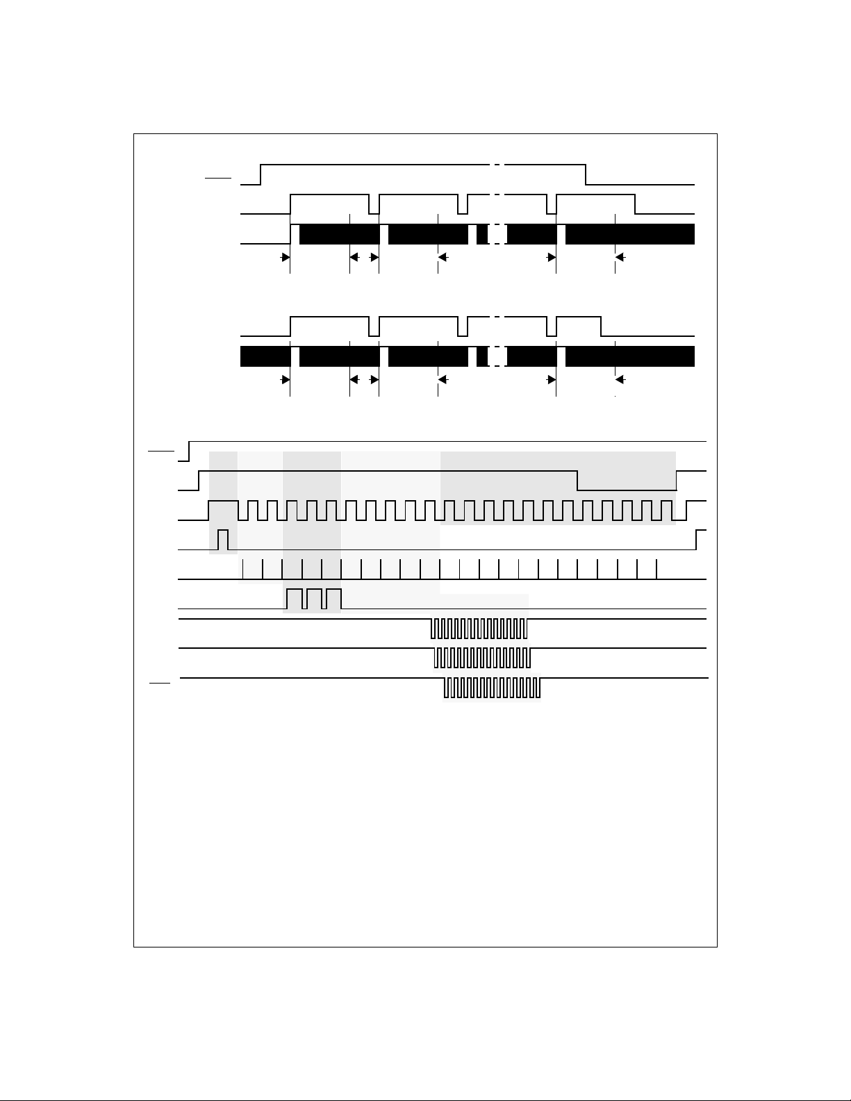
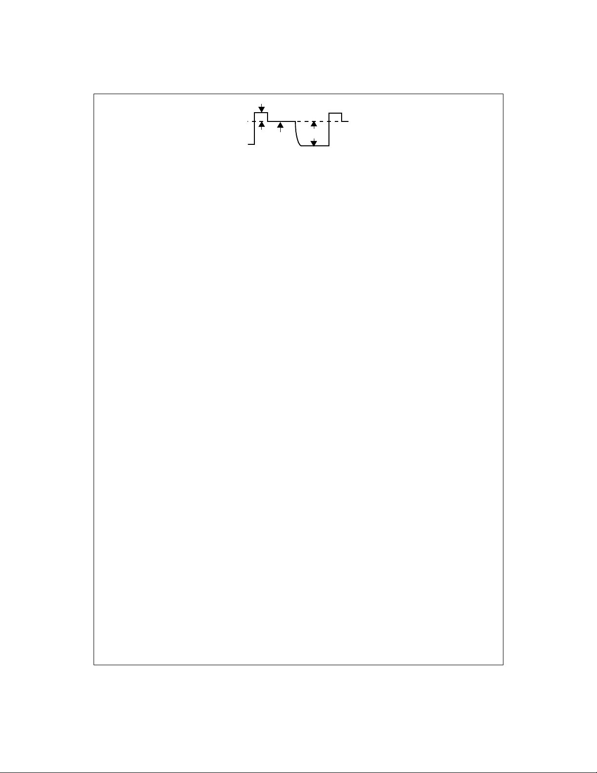
Timing Diagrams
RUN/STOP
SYNC (OUTPUT)
Ø1
SYNC (INPUT)
Ø1
RUN/
STOP
SYNC
(OUTPUT)
Ø1
TR1
Transfer
Dummy Black Valid Pix els
Line 1
Diagram 1: SYNC OUT Mode Timing, Multiple Lines
Line 1
Diagram 2: SYNC IN Mode Timing, Multiple Lines
Line 2 Line n
Line 2 Line n
Additional Integration Time
(truncated)
RS
CLAMP
OCLK
GLCK
EOC
123
Diagram 3: SYNC OUT Mode Timing, One Line
11
http://www.national.com
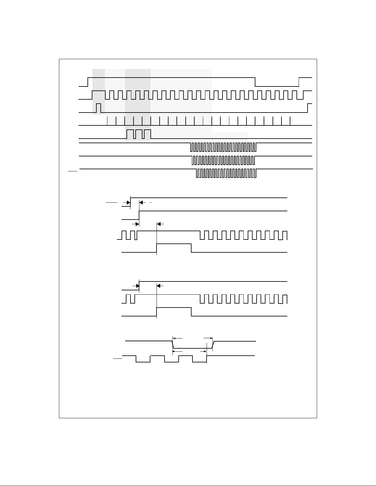
SYNC
(INPUT)
Ø1
TR1
RS
Transfer
Dummy Black Valid Pix els
CLAMP
OCLK
GLCK
EOC
RUN/STOP
SYNC (OUTPUT)
Ø1
TR1
SYNC (INPUT)
Ø1
TR1
123
Diagram 4: SYNC In Mode Timing, One Line
t
R/S START
t
START
Diagram 5: Start of Line Scan, SYNC OUT Mode, One TR Pulse
t
START
Diagram 6: Start of Line Scan, SYNC IN Mode, One TR Pulse
t
SYNC LOW
SYNC
t
SYNC END
8MCLK max
EOC
Diagram 7: Timing for End of Line/Start of Next Line
12
8MCLK min
http://www.national.com
 Loading...