

NSC LM9811CCV Datasheet
LM9811
10-Bit Greyscale/30-Bit Color
Linear CCD Sensor Processor
LM9811 10-Bit Greyscale/30-Bit Color Linear CCD Sensor Processor
April 1998
General Description
The LM9811 is a high performance integrated signal
processor/digitizer for linear CCD image scanners. The
LM9811 performs all the analog processing (correlated
double sampling for black level and offset compensation,
pixel-by-pixel gain (shading) correction, and 10-bit
analog-to-digital conversion) necessary to maximize the performance of a wide range of linear CCD sensors.
The LM9811 can be digitally programmed to work with a
wide variety of CCDs from different manufacturers. An internal configuration register sets CCD and sampling timing to
maximize performance, simplifying the design and manufacturing processes.
The LM9811 can be used with parallel output color CCDs. A
signal inversion mode eases use with CIS sensors. For
complementary voltage reference see the LM4041.
Applications
n Color and Greyscale Flatbed and Sheetfed Scanners
n Fax and Multifunction Peripherals
n Digital Copiers
n General Purpose Linear CCD Imaging
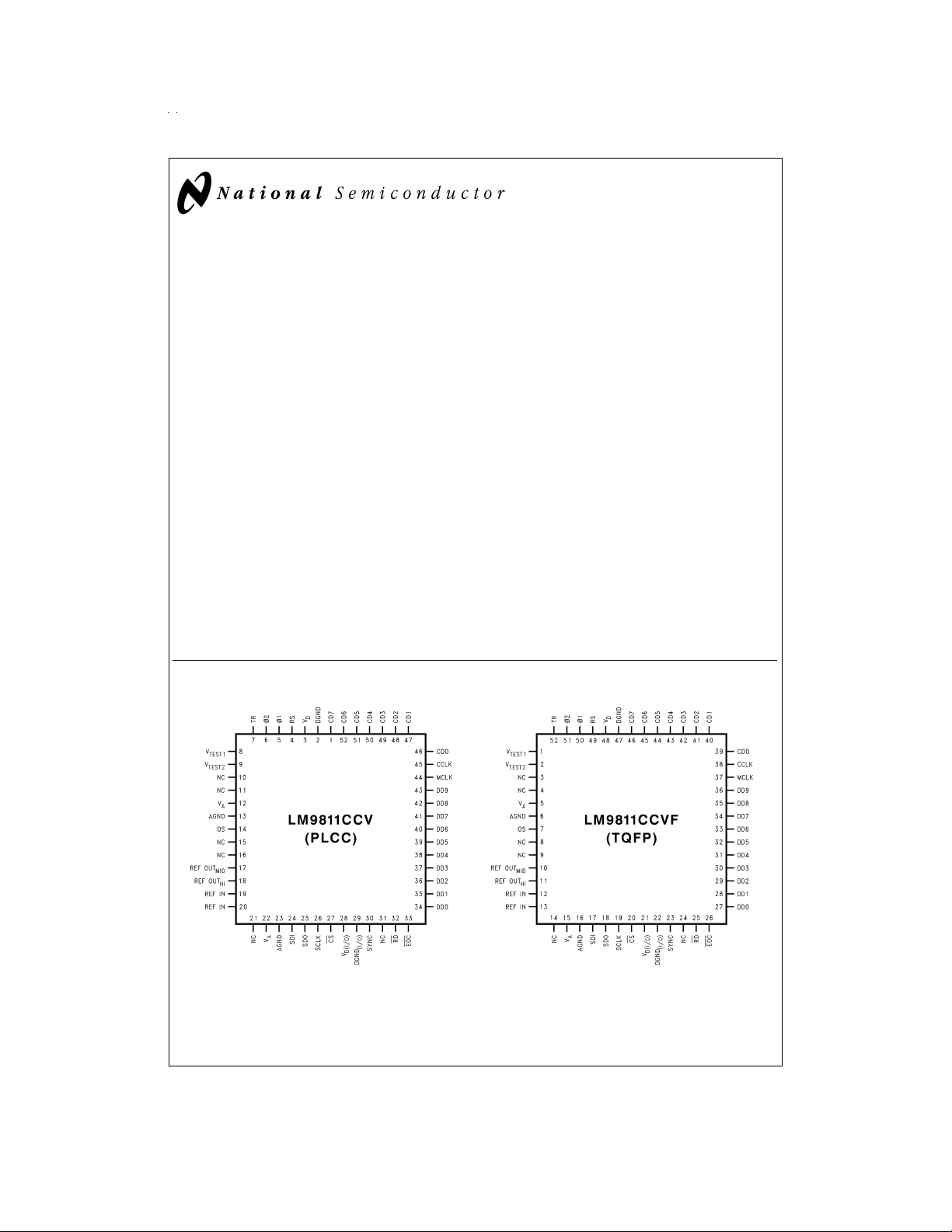
Connection Diagrams
Features
n 1.5 Million pixels/s conversion rate
n Pixel-rate shading correction for individual pixels
maximizes dynamic range and resolution, even on
“weak” pixels
n Implements Correlated Double Sampling for minimum
noise and offset error
n Reference and signal sampling points digitally controlled
in 40ns increments for maximum performance
n Generates all necessary CCD clock signals
n Compatible with a wide range of linear CCDs
n Supports some Contact Image Sensors (CIS)
n TTL/CMOS input/output compatible
Key Specifications
n Resolution: 10 Bits
n Pixel Conversion Rate: 1.5MHz
n Supply Voltage: +5V
n Supply Voltage
(Digital I/O): +3.3V
n Power Dissipation: 260mW (max)
±
10%or +5V±5
±
5
%
%
DS012813-1 DS012813-2
TRI-STATE®is a registeredtrademark of National Semiconductor Corporation.
™
MICROWIRE
SPI
© 1999 National Semiconductor Corporation DS012813 www.national.com
is a trademark of National Semiconductor Corporation.
™
is a trademark of Motorola, Inc.
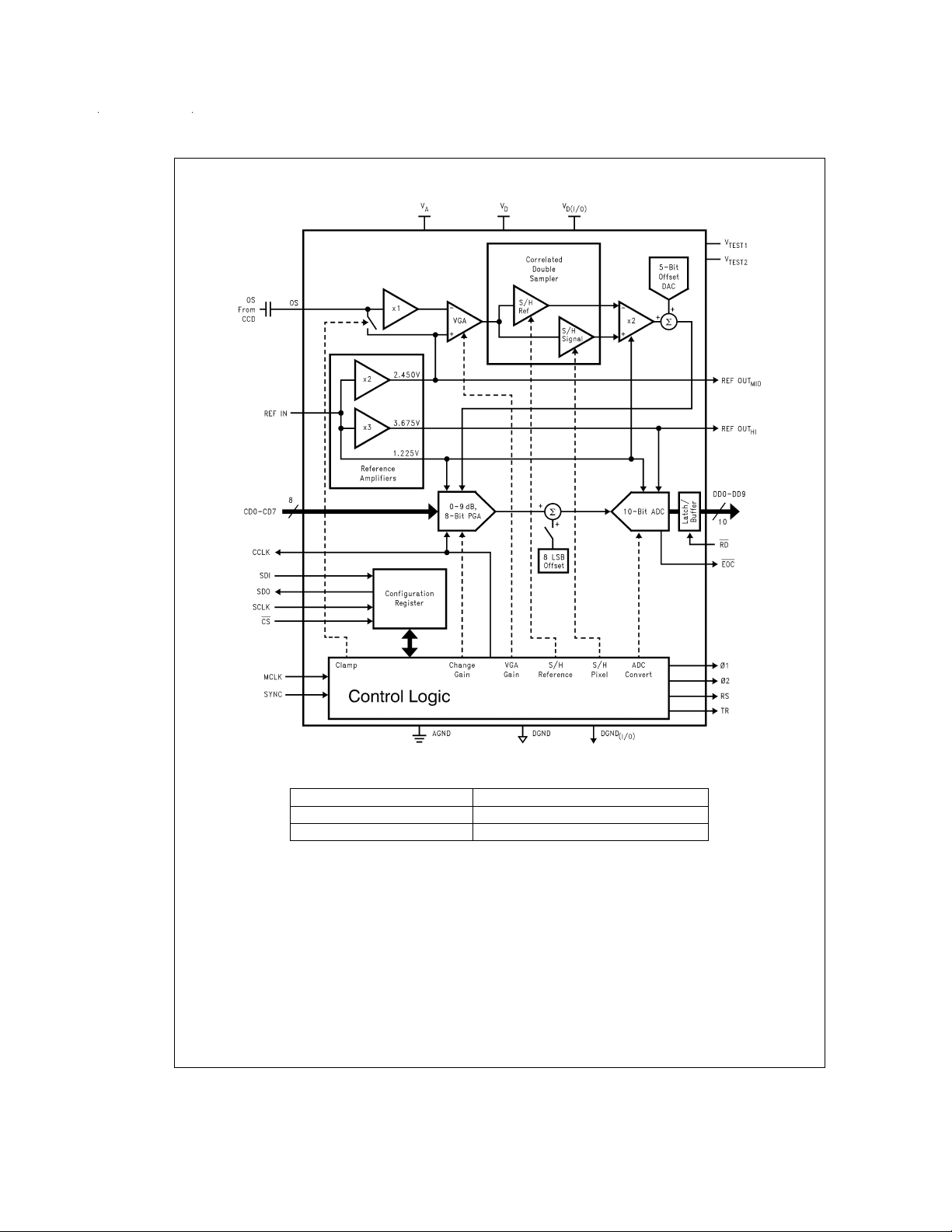
Block Diagram
Ordering Information
Commercial (0˚C ≤ TA≤ +70˚C) Package
LM9811CCV V52A 52-Pin Plastic Leaded Chip Carrier
LM9811CCVF VEG52A 52-Pin Thin Quad Flatpack
www.national.com 2
DS012813-3
Absolute Maximum Ratings (Notes 1, 2)
+
=
=
=
Positive Supply Voltage (V
V
V
A
D
with Respect to
GND=AGND=DGND=DGND
(I/O)
Voltage on any Input or Output Pin 0.3V to V
Input Current at any Pin (Note 3)
Package Input Current (Note 3)
=
Package Dissipation at T
25˚C (Note 4)
A
ESD Susceptibility (Note 5)
Human Body Model 2000V
Soldering Information (Note 6)
Infrared, 10 seconds
LM9811CCV 300˚C
)
V
D(I/O
6.5V
+
+0.3V
±
25 mA
±
50 mA
Operating Ratings (Notes 1, 2)
Operating Temperature
Range T
LM9811CCV, LM9811CCVF 0˚C ≤ TA≤ +70˚C
Supply Voltage +4.75V to +5.25V
V
A
Supply Voltage +4.75V to +5.25V
V
D
Supply Voltage +2.7V to +5.25V
V
D(I/O)
| ≤ 100 mV
|V
A–VD
V
A–VD(I/O)
OS, REF IN Voltage Range −0.05V to V
CD0–CD7, MCLK, SYNC,
SDI, SCLK, CS, RD,
Voltage Range −0.05V to V
MIN
D(I/O)
≤ TA≤ T
≥ −100 mV
+ 0.05V
A
+ 0.05V
LM9811CCVF 220˚C
Storage Temperature −65˚C to +150˚C
Electrical Characteristics
=
The following specifications apply for AGND=DGND=DGND(I/O)=0V, V
REF IN=+1.225V
apply for T
DC,fMCLK
=
=
T
A
J
=
20MHz, R
to T
T
MIN
MAX
=
25Ω. All LSB units are ADC LSBs unless otherwise specified. Boldface limits
S
; all other limits T
=
A
=
T
25˚C. (Note 8)
J
=
V
A
+5.0V
D
DC,VD(I/O)
Symbol Parameter Conditions Typical Limits Units
(Note 9) (Note 10) (Limits)
CCD SOURCE REQUIREMENTS FOR FULL SPECIFIED ACCURACY AND DYNAMIC RANGE (Note 11)
V
WHITE
Maximum Peak CCD Differential VGA Gain=0dB 1.1 V (min)
Signal Range VGA Gain=9dB 0.4 V (min)
V
RFT
Maximum CCD Reset FeedThrough
Amplitude
ADC CHARACTERISTICS (Note 16)
Resolution with No Missing Codes f
ILE Integral Linearity Error (Note 12) f
DNL Differential Non-Linearity f
=
12MHz 9 Bits (min)
MCLK
=
12MHz
MCLK
=
12MHz +2.0 LSB (max)
MCLK
PGA CHARACTERISTICS
Monotonicity 8 Bits (min)
=
+5.0 or +3.0V
,
DC
2 V (min)
+4.0 LSB (max)
−3.0 LSB (min)
MAX
PGA Adjustment Range
Gain Error at any Gain (Note 14) 1.4
VGA CHARACTERISTICS
Monotonicity 4 Bits (min)
VGA Adjustment Range
Gain Error at any Gain (Note 15)
OFFSET TRIM CHARACTERISTICS
Offset DAC LSB Size In Units of ADC LSBs 1.7 LSB
Offset DAC DNL In Units of Offset DAC LSBs
Offset Add Magnitude In Units of ADC LSBs 8
SYSTEM CHARACTERISTICS
Full Channel Gain Error VGA Gain=1, PGA Gain=1
Pre-PGA Offset Error (In ADC LSBs) VGA Gain=1, Offset DAC=0
Post-PGA Offset Error (In ADC LSBs) Offset Add=0
REFERENCE AND ANALOG INPUT CHARACTERSTICS (Note 7)
OS Input Capacitance 5 pF
2.95 2.8 V/V (min)
%
(max)
8.95 8.5 dB (min)
±
0.15 dB (max)
±
0.25
±
0.9 LSB
6.4 LSB (min)
10.0 LSB (max)
±
0.6
±
4 LSB
±
4 LSB
±
3.0
%
(max)
www.national.com3
Electrical Characteristics (Continued)
=
The following specifications apply for AGND=DGND=DGND(I/O)=0V, V
REF IN=+1.225VDC,f
apply for T
=
=
T
A
J
=
20MHz, R
MCLK
to T
T
MIN
MAX
=
25Ω. All LSB units are ADC LSBs unless otherwise specified. Boldface limits
S
; all other limits T
=
A
=
T
25˚C. (Note 8)
J
=
V
A
+5.0V
D
DC,VD(I/O)
Symbol Parameter Conditions Typical Limits Units
(Note 9) (Note 10) (Limits)
REFERENCE AND ANALOG INPUT CHARACTERSTICS (Note 7)
OS Input Leakage Current Measured with OS=2.45V
R
REF
ADC Reference Ladder (REF OUT
to REF IN) Impedance 2000 Ω (max)
HI
DC
950
REF IN Reference Voltage (Note 13) 1.225
=
+5.0 or +3.0V
,
DC
2 20 nA (max)
500 Ω (min)
1.19 V (min)
1.26 V (max)
DC and Logic Electrical Characteristics
The following specifications apply for AGND=DGND=DGND
IN=+1.225V
25˚C.
DC,fMCLK
=
20MHz, R
=
25Ω. Boldface limits apply for T
s
(I/O)
=
Symbol Parameter Conditions Typical Limits Units
CD0–CD7, MCLK, SYNC, SDI, SCLK, CS , RD DIGITAL INPUT CHARACTERISTICS
=
V
5.25V 2.0 V (min)
V
IN(1)
V
IN(0)
I
IN
C
IN
Logical “1” Input Voltage
Logical “0” Input Voltage
Input Leakage Current
Input Capacitance 5 pF
D(I/O)
=
V
3.6V 2.0 V (min)
D(I/O)
=
V
4.75V 0.8 V (max)
D(I/O)
=
V
2.7V 0.7 V (max)
D(I/O)
=
V
V
IN
D
=
V
DGND −0.1 µA
IN
DD0–DD9, EOC , CCLK, SDO DIGITAL OUTPUT CHARACTERISTICS
=
V
4.75V, I
V
V
I
C
OUT
OUT(1)
OUT(0)
OUT
D(I/O)
=
V
Logical “1” Output Voltage
Logical “0” Output Voltage
TRI-STATE®Output Current V
(DD0–DD9 only) V
D(I/O)
=
V
D(I/O)
=
V
D(I/O)
=
V
D(I/O)
=
V
D(I/O)
=
OUT
=
OUT
TRI-STATE Output Capacitance 5 pF
OUT
4.75V, I
OUT
2.7V, I
OUT
2.7V, I
OUT
5.25V, I
OUT
3.6V, I
OUT
DGND 0.1 µA
V
D
φ1, φ2, RS, TR DIGITAL OUTPUT CHARACTERISTICS
V
V
OUT(1)
OUT(0)
Logical “1” Output Voltage
Logical “0” Output Voltage V
=
V
4.75V, I
D
=
V
4.75V, I
D
=
5.25V, I
D
OUT
OUT
OUT
=
=
=
POWER SUPPLY CHARACTERISTICS
I
A
I
D
I
D(I/O)
Analog Supply Current
Digital Supply Current
Digital I/O Supply Current
Operating 25 38 mA (max)
Standby 50 µA
Operating 6 8 mA (max)
Standby 65 µA
Operating, V
Operating, V
Standby, V
=
D(I/O)
=
D(I/O)
=
5.0V or 3.0V 1.7 mA
D(I/O)
=
0V, V
=
V
A
A
+5.0V
D
=
=
T
J
DC,VD(I/O)
to T
T
MIN
=
; all other limits T
MAX
+5.0 or +3.0V
A
, REF
DC
=
=
T
J
(Note 9) (Note 10) (Limits)
0.1 µA
=
−360 µA 2.4 V (min)
=
−10 µA 4.4 V (min)
=
−360 µA 2.1 V (min)
=
−10 µA 2.5 V (min)
=
1.6 mA 0.4 V (max)
=
1.6 mA 0.4 V (max)
−0.1 µA
−360 µA 2.4 V (min)
−10 µA 4.4 V (min)
1.6 mA 0.4 V (max)
5.0V 3.1 6 mA (max)
3.0V 1.6 4 mA (max)
www.national.com 4
AC Electrical Characteristics, MCLK Independent
The following specifications apply for AGND=DGND=DGND
f
MCLK
=
T
MIN
=
20MHz, t
to T
MAX
=
1/f
MCLK
; all other limits T
MCLK,tr
=
=
t
f
=
=
T
A
J
5ns, R
25˚C.
s
=
25Ω,C
=
(I/O)
(databus loading)=50 pF/pin. Boldface limits apply for T
L
Symbol Parameter Conditions Typical Limits Units
f
MCLK
Maximum MCLK Frequency (Note 16) 20 MHz (min)
Minimum MCLK Frequency 1 MHz (max)
MCLK Duty Cycle
t
A
t
CDSETUP
t
CDHOLD
t
D1H,tD0H
t
DACC
f
SCLK
SYNC Setup of MCLK 5 10 ns (min)
Correction Data Valid to CLK Setup 14 20 ns (min)
Correction Data Valid to CLK Hold −12 0 ns (min)
RD High to DD0–DD9 TRI-STATE 5 15 ns (max)
Access Time Delay from RD Low to
DD0–DD9 Data Valid
Maximum SCLK Frequency 8 MHz (min)
SCLK Duty Cycle
t
SDI
t
HDI
t
DDO
t
HDO
t
DELAY
t
SETUP
t
S1H,tS0H
t
RDO
t
FDO
SDI Set-Up Time from SCLK
Rising Edge
SDI Hold Time from SCLK
Rising Edge
Delay from SCLK Falling Edge to
SDO Data Valid
SDO Hold Time from SCLK
Falling Edge
=
3k, C
R
L
DELAY from SCLK Falling Edge to CS
Rising or Falling Edge
Set-Up Time of CS Rising or Falling
Edge to SCLK Rising Edge
Delay from CS Rising Edge to SDO
TRI-STATE
SDO Rise Time, TRI-STATE to High
SDO Rise Time, Low to High 20 ns
SDO Fall Time, TRI-STATE to Low
SDO Fall Time, High to Low 20 ns
=
R
3k, C
L
=
3k, C
R
L
=
3k, C
R
L
=
=
0V, V
V
A
D
=
V
D(I/O)
, REF IN=+1.225VDC,
+5.0V
DC
(Note 9) (Note 10) (Limits)
30 40
70 60
15 30 ns (max)
40
60
3 10 ns (min)
2 15 ns (min)
25 55 ns (max)
=
25pF 30
L
55 ns (max)
5 ns (min)
5 10 ns (min)
0 10 ns (min)
=
50pF 25 50 ns (max)
L
=
50pF
L
=
50pF
L
20 ns
20 ns
%
%
%
%
=
A
(min)
(max)
(min)
(max)
T
J
AC Electrical Characteristics, MCLK Dependent
The following specifications apply for AGND=DGND=DGND
=
f
20MHz, t
MCLK
Register Parameters for limits labelled C.R. Boldface limits apply for T
25˚C.
MCLK
=
1/f
MCLK,tr
=
=
t
f
5ns, R
s
=
25Ω,C
=
(I/O)
(databus loading)=50 pF/pin. Refer to
L
Symbol Parameter Conditions Typical Limits Units
t
START
t
φ
t
TRWIDTH
t
GUARD
t
RSWIDTH
t
RS
MCLK to first φ1 High 50ns 1 t
φ1, φ2 Clock Period
Standard CCD Mode 400ns 8 t
Even/Odd CCD Mode 800ns 16 t
Transfer Pulse (TR) Width C.R. µs
φ1 to TR, TR to φ1 Guardband C.R. ns
Reset Pulse (RS) Width C.R. ns
Falling Edge of φ1 to RS Standard CCD Mode
Either Edge of φ1 to RS Even/Odd CCD Mode
0V, V
=
=
V
A
D
=
=
T
A
J
=
V
D(I/O)
to T
T
MIN
MAX
, REF IN=+1.225VDC,
+5.0V
DC
Table 2
; all other limits T
. Configuration
=
A
(Note 9) (Note 10) (Limits)
C.R. ns
www.national.com5
T
J
MCLK
MCLK
MCLK
=
AC Electrical Characteristics, MCLK Dependent (Continued)
The following specifications apply for AGND=DGND=DGND
=
f
20MHz, t
MCLK
Register Parameters for limits labelled C.R. Boldface limits apply for T
25˚C.
MCLK
=
1/f
MCLK,tr
=
=
t
f
5ns, R
=
s
25Ω,C
=
(I/O)
(databus loading)=50 pF/pin. Refer to
L
Symbol Parameter Conditions Typical Limits Units
t
S/HREF
t
S/HSIG
t
S/HWIDTH
t
SYNCLOW
t
B
t
CCLKWIDTH
t
DATAVALID
t
EOCWIDTH
Falling Edge of φ1 to Ref. Sample Standard CCD Mode
Either Edge of φ1 to Ref. Sample Even/Odd CCD Mode
Falling Edge of φ1 to Sig. Sample Standard CCD Mode
Either Edge of φ1 to Sig. Sample Even/Odd CCD Mode
Sample Pulse Width
(Acquisition Time)
SYNC Low Between Lines 100ns 2 t
SYNC Setup of φ1 to End Line 2 t
CCLK Pulse Width 250ns 5 t
Data Valid Time from EOC Low 300 ns (min)
EOC Pulse Width 250ns 5 t
φ1 and φ2 Frequency
Standard CCD Mode 2.5MHz f
Even/Odd CCD Mode 1.25MHz f
φ1 and φ2 Duty Cycle 50
0V, V
=
=
V
A
D
=
=
T
A
J
=
V
D(I/O)
to T
T
MIN
MAX
, REF IN=+1.225VDC,
+5.0V
DC
Table 2
; all other limits T
. Configuration
=
T
A
J
(Note 9) (Note 10) (Limits)
C.R. ns
C.R. ns
50ns 1 t
/8 Hz
MCLK
/16 Hz
MCLK
MCLK
MCLK
MCLK
MCLK
MCLK
%
Electrical Characteristics (Notes)
Note 1: Absolute Maximum Ratings indicate limits beyond which damage to the device may occur. Operating Ratings indicate conditions for which the device is
functional, but do not guarantee specific performance limits. For guaranteed specifications and test conditions, see the Electrical Characteristics. The guaranteed
specifications apply only for the test conditions listed. Some performance characteristics may degrade when the device is not operated under the listed test conditions.
Note 2: All voltages are measured with respect to GND=AGND=DGND=DGND
Note 3: When the input voltage (V
The 50 mA maximum package input current rating limits the number of pins that can simultaneously safely exceed the power supplies with an input current of 25
mA to two.
Note 4: The maximum power dissipation must be derated at elevated temperatures and is dictated by T
allowable power dissipation at any temperature is P
mounted is 52˚C/W for the V52A PLCC package, and 70˚C/W for the VEG52A TQFP package.
Note 5: Human body model, 100pF capacitor discharged through a 1.5 kΩ resistor.
Note 6: See AN450 “Surface Mounting Methods and Their Effect on Product Reliability” or the section titled “Surface Mount” found in any National Semiconductor
Linear Data Book for other methods of soldering surface mount devices.
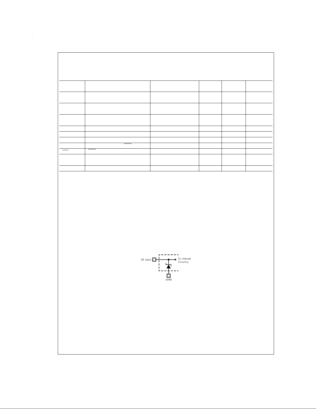
Note 7: AZener diode clamps the OS analog input to AGND as shown below. This input protection, in combination with the external clamp capacitor and the output
impedance of the CCD, prevents damage to the LM9811 from transients during power-up.
) at any pin exceeds the power supplies (V
IN
=
D
(T
Jmax–TA
)/θJA.T
Jmax
=
0V, unless otherwise specified.
(I/O)
<
GND or V
IN
=
150˚C for this device. The typical thermal resistance (θ
>
VAor VD), the current at that pin should be limited to 25 mA.
IN
, θJAand the ambient temperature, TA. The maximum
Jmax
) of this part when board
JA
=
(min)
(max)
Note 8: Toguarantee accuracy, it is required that V
Note 9: Typicals are at T
Note 10: Tested limits are guaranteed to National’s AOQL (Average Outgoing Quality Level).
=
=
T
25˚C, f
J
A
and VDbe connected together to the same power supply with separate bypass capacitors at each supply pin.
A
=
20MHz, and represent most likely parametric norm.
MCLK
www.national.com 6
DS012813-4
Electrical Characteristics (Notes) (Continued)
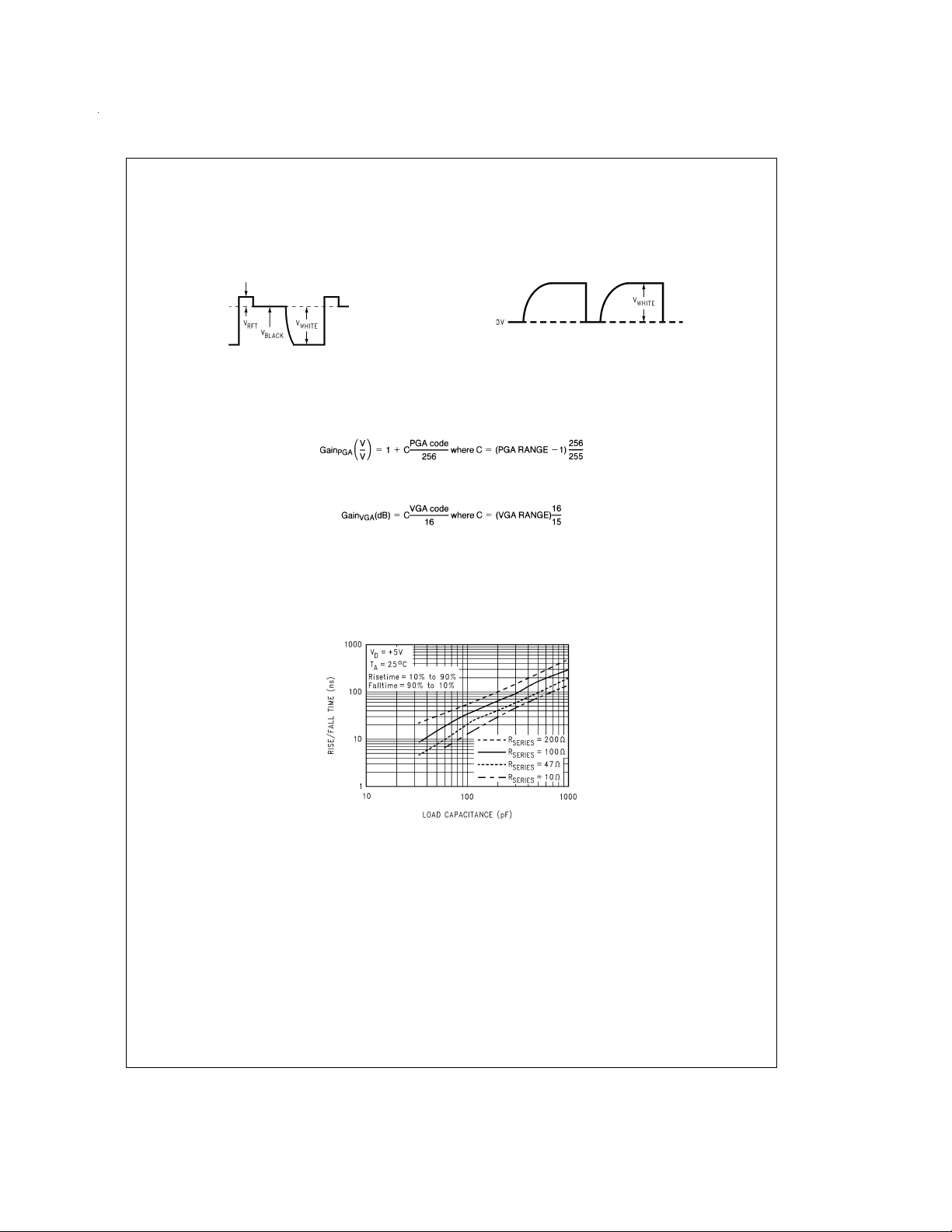
Note 11: For CCDs, V
pixel output voltage for a white (full scale) image with respect to the reference level, V
reset feedthrough pulse. For CIS, V
correctable range of pixel-to-pixel V
the LM9811 can correct for using its internal PGA.
is defined as the CCD OS voltage for the reference period following the reset feedthrough pulse. V
BLACK
is defined as the peak CCD pixel output voltage for a white (full scale) image with respect to GND (0V). The maximum
WHITE
variation is defined as the maximum variation in V
WHITE
BLACK-VRFT
WHITE
is defined as the peak CCD
is defined as the peak positive deviation above V
(due to PRNU, light source intensity variation, optics, etc.) that
WHITE
BLACK
of the
CCD Output Signal
DS012813-5
Note 12: Integral linearity error is defined as the deviation of the analog value, expressed in LSBs, from the straight line that best fits the actual transfer function
of the ADC.
Note 13: Reference voltages below 1.19V may decrease SNR. Reference voltages above 1.26V may cause clipping errors inside the LM9811. The
LM4041EIM3-1.2 (SOT-23 package) or the LM4041EIZ-1.2 (TO-92 package) bandgap voltage references are recommended for this application.
Note 14: PGA Gain Error is the maximum difference between the measured gain for any PGA code and the ideal gain calculated by using the formula
Note 15: VGA Gain Error is the maximum difference between the measured gain for any VGA code and the ideal gain calculated by using the formula
Note 16: ADC Characteristics (Resolution, INL and DNL) are guaranteed for f
except ADC Characteristics, which will be approximately 8 bits.
and PGA RANGE=the PGA adjustment range (in V/V) of the LM9811 under test.
and VGA RANGE=the VGA adjustment range (in dB) of the LM9811 under test.
up to 12MHz. For 12MHz<f
MCLK
CIS Output Signal
≤ 20 MHz, all specifications are guaranteed
MCLK
DS012813-6
Typical Performance Characteristics
φ1, φ2, RS, and TR Rise and Fall Times
Through a Series Resistance vs Load Capacitance
DS012813-8
www.national.com7
Pin Descriptions
CCD Driver Signals
φ1 Digital Output. CCD clock signal, phase
φ2 Digital Output. CCD clock signal, phase
RS Digital Output. Reset pulse for the CCD.
TR Digital Output. Transfer pulse for the
OS Analog Input. This is the OS (Output
REF IN Analog Inputs. These two pins are the
REF OUT
REF OUT
,
V
TEST1
V
TEST2
SDI Digital Input. Serial Data Input pin.
SDO Digital Output. Serial Data Output pin.
SCLK Digital Input. This is the serial data
CS
CD0 (LSB)–
CD7 (MSB)
1.
2.
CCD.
Analog I/O
Signal) from the CCD. The maximum
peak signal that can be accurately
digitized is equal to the voltage at REF
IN, typically 1.225V.
system reference voltage inputs and
should be tied together to a 1.225V
voltage source and bypassed to AGND
with a 0.1 µF monolithic capacitor.
Analog Output. This reference voltage is
HI
developed internally by the LM9811,
and is equal to 3 times REF IN. It
should be bypassed to AGND with a
0.1 µF monolithic capacitor.
Analog Output. This reference voltage is
MID
developed internally by the LM9811,
and is equal to 2 times REF IN. It
should be bypassed to AGND using a
0.1 µF monolithic capacitor.
Analog Inputs/Outputs. These pins are
used for testing the device during
manufacture and should be left
unconnected.
Configuration Register I/O
clock, used to clock data in through SDI
and out through SDO. SCLK is
asynchronous to MCLK. Input data is
latched and output data is changed on
the rising edge of SCLK.
Digital Input. This is the Chip Select
signal for writing to the Configuration
Register through the serial interface.
This input must be low in order to
communicate with the Configuration
Register. This pin is used for serial I/O
only–it has no effect on any other
section of the chip.
Digital Coefficient I/O
Digital Inputs. Correction Coefficient
Databus. This is the 8-bit data path for
the gain adjust PGA, used during line
scan.
CCLK Digital Output. This is the signal that is
used to clock the Gain coefficients into
the LM9811. Data is latched on the
rising edge of CCLK.
Digital Output I/O
DD0 (LSB)–
DD9 (MSB)
Digital Outputs. Pixel Output Databus.
This data bus outputs the 10-bit digital
output data during line scan.
EOC
Digital Output. This is the End of
Conversion signal from the ADC
indicating that new pixel data is
available.
RD
Digital Input. Taking this input low
places the data stored in the output
latch on the bus. When this input is high
the DD0–DD9 bus is in TRI-STATE.
General Digital I/O
MCLK Digital Input. This is the 12MHz (typical)
master system clock.
SYNC Digital Input. A low-to-high transition on
this input begins a line scan operation.
The line scan operation terminates
when this input is taken low.
Analog Power
V
A
This is the positive supply pin for the
analog supply. It should be connected
to a voltage source of +5V and
bypassed to AGND with a 0.1 µF
monolithic capacitor in parallel with a
10 µF tantalum capacitor.
AGND This is the ground return for the analog
supply.
Digital Power
V
D
This is the positive supply pin for the
digital supply. It should be connected to
a voltage source of +5V and bypassed
to DGND with a 0.1 µF monolithic
capacitor.
DGND This is the ground return for the digital
supply.
V
D(I/O)
This is the positive supply pin for the
digital supply for the LM9811’s I/O. It
should be connected to a voltage
source of +3V to +5V and bypassed to
DGND
capacitor. If the supply for this pin is
different than the supply for V
it should also be bypassed with a 10 µF
with a 0.1 µF monolithic
(I/O)
and VD,
A
tantalum capacitor.
DGND
(I/O)
This is the ground return for the digital
supply for the LM9811’s I/O.
NC
NC All pins marked NC (no connect) should
be left floating. Do not tie NC pins to
ground., power supplies, or any other
potential or signal.
www.national.com 8
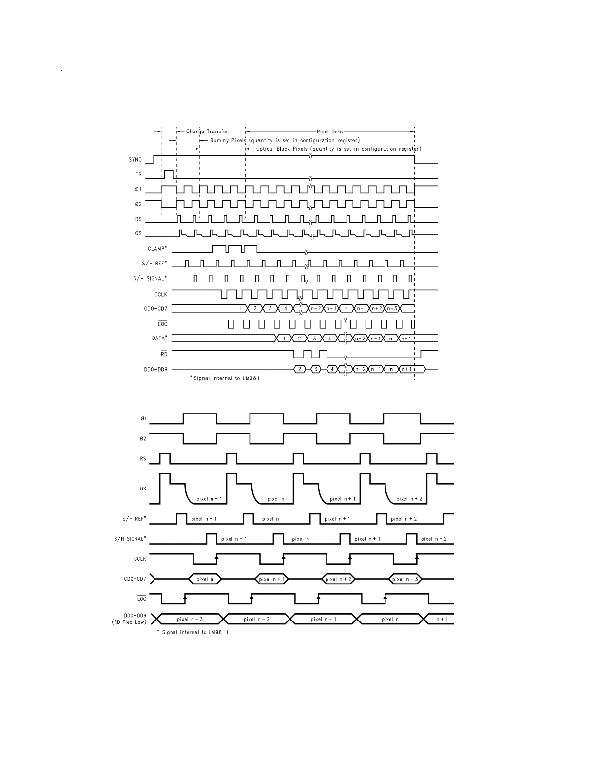
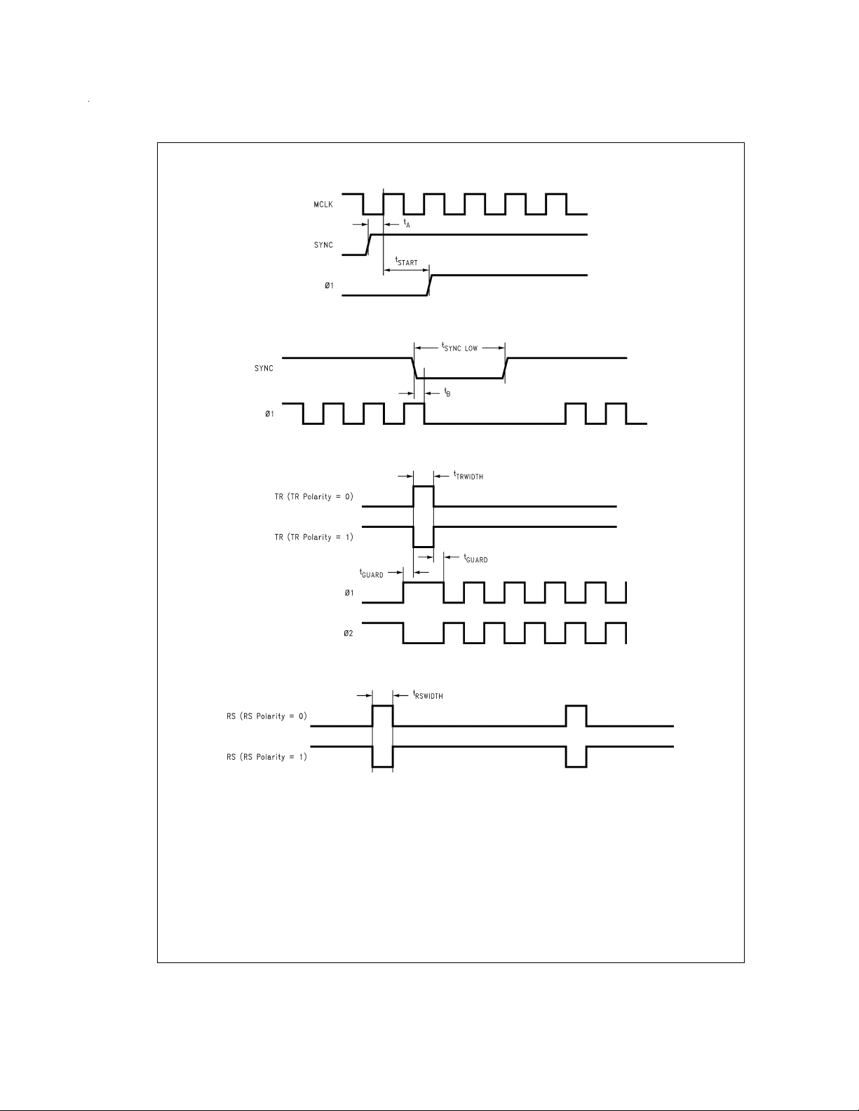
Timing Diagrams
DS012813-9
FIGURE 1. Line Scan Timing Overview
FIGURE 2. Pixel Pipeline Timing Overview
DS012813-10
www.national.com9
Timing Diagrams (Continued)
FIGURE 4. Timing for End of Line/Start of Next Line
DS012813-11
FIGURE 3. Timing for Start of Line Scan
DS012813-12
FIGURE 5. TR Pulse Timing
FIGURE 6. RS Pulse Polarity
www.national.com 10
DS012813-13
DS012813-14
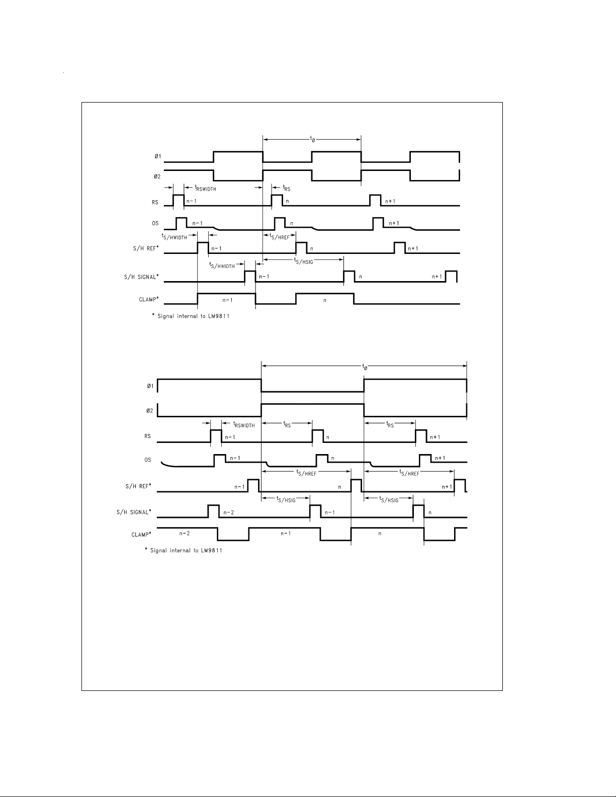
Timing Diagrams (Continued)
Note: Clamp signal only active during optical black pixels at beginning of line.
FIGURE 7. CCD Timing
Note: Clamp signal only active during optical black pixels at beginning of line.
FIGURE 8. CCD Timing (Even/Odd CCDs)
DS012813-15
DS012813-16
www.national.com11
 Loading...