

NSC LM9810CCWM Datasheet
N
LM9810/20 10/12-Bit Image Sensor Processor Analog Front End
General Description
The LM9810 and LM 9820 are high performance Ana log Front
Ends (AFEs) for image sensor processing systems. The
LM9810/20 perform s all the analog and mixed signal func tions
(correlated double s ampling, color s pecific gain and offset correction, and analog to digital conversion) necessar y to digitize
the output of a wide variety of CIS and CCD sensors. The
LM9810 has a 10 bit 6M Hz ADC, and the LM982 0 has a 12 bit
6MHz ADC. The LM98 10 and L M9820 a re pin-for-pin and functionally compatible.
Applications
•
Color Flatbed Document Scanners
•
Color Sheetfed Scanners
•
Multifunction Imaging Product s
•
Digital Copiers
•
General Purpose Linear CCD Imaging
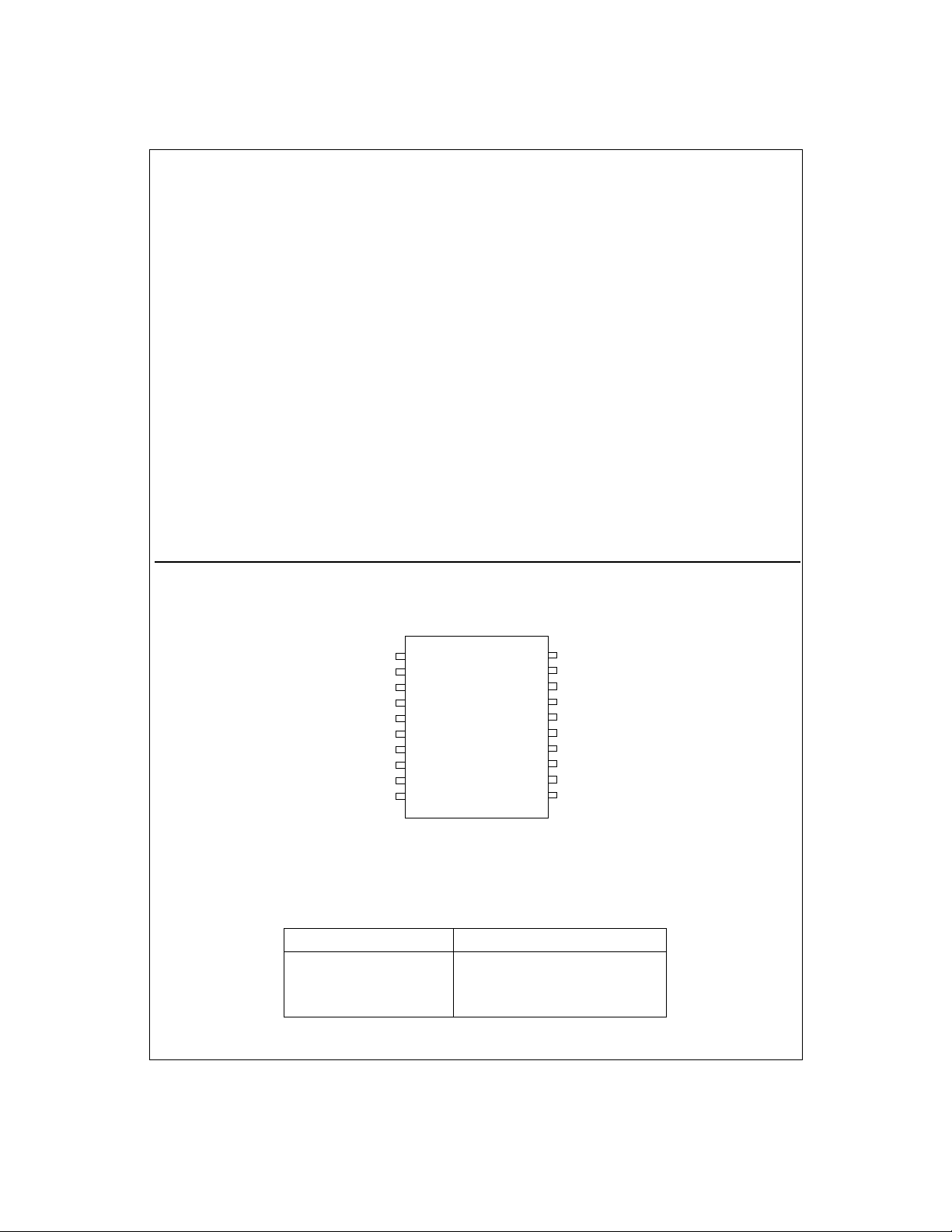
Connection Diagrams
Features
•
6 million pixels/s conversion rate
•
Digitally programm ed gain and offset for red, green and blue
pixels
•
Correlated Double Sampling for lowest noise
•
TTL/CMOS input/output compatible
Key Specifications
•
Output Data Resolution 10/12 Bits
•
Pixel Conversion Rate 6MHz
•
Supply Voltage 5V±5%
•
Power Dissi pation 300mW
LM9810/20 10/12-Bit Image Sensor Processor Analog Front End
July 1998
V
1
REF-
V
REFMID
RefBypass
SampCLK
V
REF+
OS
OS
OS
AGND
2
3
LM9810
4
5
R
6
G
7
B
VA
8
9
10
LM9820
Ordering Information
Commercial (0°C ≤ TA ≤ +70°C) Package
LM9810CCWM
LM9810CCWMX
LM9820CCWM
LM9820CCWMX
TRI-STATE® is a registered trademark of National Semiconductor Corporation.
©1997,1998 National Semiconductor Corporation
DGND
20
VD
19
MCLK
18
D5
17
D4
&
20 Pin Wide SOIC
20 Pin Wide SOIC, Tape & Reel
20 Pin Wide SOIC
20 Pin Wide SOIC, Tape & Reel
16
15
14
13
12
11
D3
D2 (SCLK)
D1 (Latch)
D0 (SDI)
NewLine
1
http://www.national.com
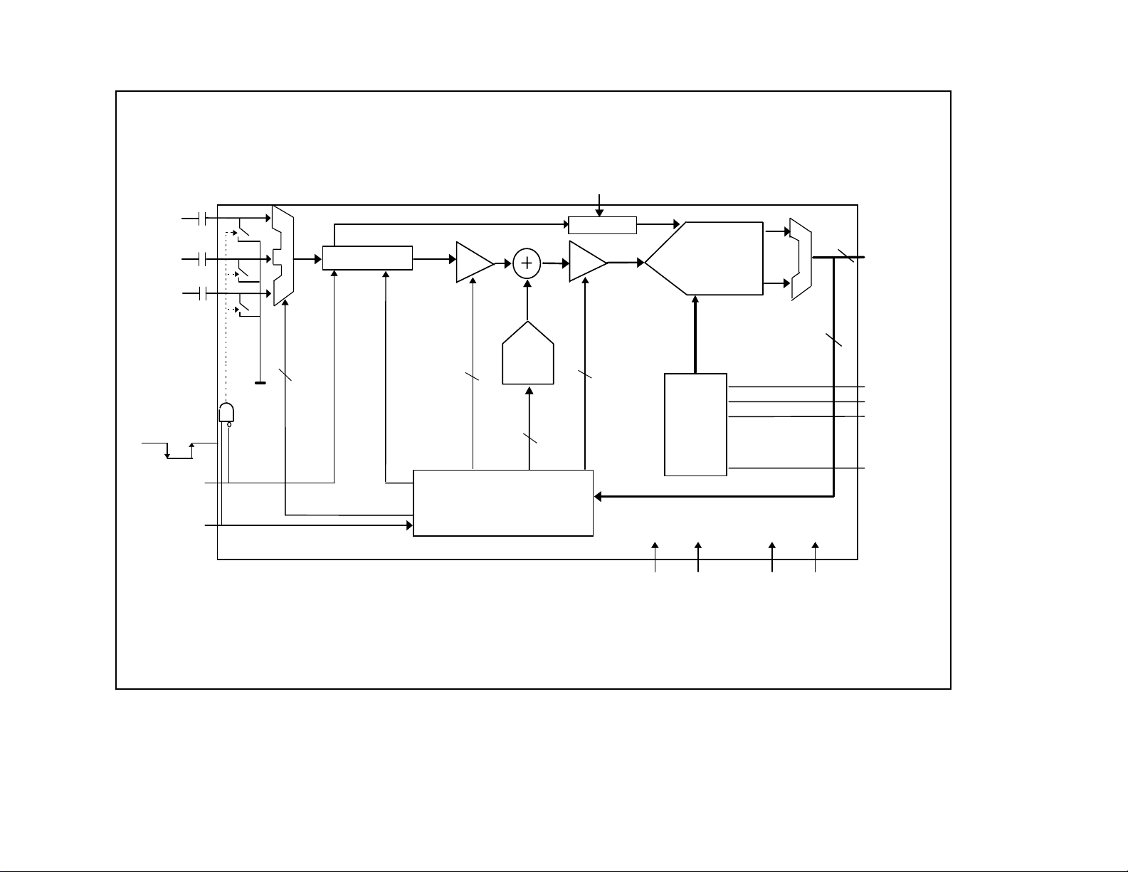
Block Diagram
MCLK
OS
R
OS
G
OS
B
V
signal
V
SampCLK
NewLine
SampCLK
M
U
X
2
V
REF+
or
V
Mux
Select
-
Sampler
0 to 2V
V
Sampling
Mode
SIG
x3 Boost
Gain of
1 or 3
x3
Offset
1
DAC
Offset
6
ADC Clock
PGA
.93 to 3
PGA Gain
5
10/12 bit
6MH z
ADC
Bandgap
Voltage
Reference
M
U
D2,D1,D0
programming
interface
6
D5-D0
3
V
REF+
V
REFMID
V
REF-
RefBypass
Configuration Register
Sampling Mode,
Offset & Gain for R,G,B
VA
AGNDDGND
VD
http://www.national.com
(
)
(
)
(
)
Absolute Maximum Ratings
(Notes 1 & 2)
Positive Supply Voltage (V+=VA=VD)
With Respect to GND=
Voltage On Any Input or Output Pin -0.3V to V
Input Current at any pin
Package Input Current
Package Dissipation at T
ESD Susceptibility
AGND=DGND
(Note 3)
(Note 3)
A
(Note 5)
= 25°C
+
±25mA
±50mA
(Note 4)
Human Body Model 2000V
+0.3V
Operating Ratings
Operating Temperature Range T
6.5V
VA
Supply Voltage +4.75V to +5.25V
VD
Supply Voltage +4.75V to +5.25V
VA-VD
|
|
OS
, OSG, OS
R
Input Voltage Range -0.05V to VA + 0.05V
NewLine, SampCLK, D0-D2, MCLK
Input Voltage Range -0.05V to
Soldering Information
Infrared, 10 second s
(Note 6)
300°C
Storage Temperature -65°C to +150°C
Electrical Characteristics
The following specifications apply for
T
A=TJ=TMIN
to T
; all other limits TA=TJ=25°C.
MAX
AGND=DGND
=0V, VA=VD=+5.0V
(Notes 7, 8, & 12)
Symbol Parameter Conditions
CCD/CIS Source Requirements for Full Specified Accuracy and Dynamic Range
V
OS
Sensor’s Maximum Peak Differential
PEAK
Signal Range
Gain = 0.933
Gain = 3.0
Gain = 9.0
Analog Input Characteristics
OS
OS
OS
,
,
R
Input Capacitance 5 pF
G
B
Measured with OS = 3.5V
OS
OS
OS
,
,
R
Input Leakage Current
G
B
CDS disabled, selected OS input
CDS disabled, unselected OS
input
Coarse Color Balance PGA Characteristics
Monotonicity 5 bits (min)
G
(Minimum PGA Gain) PGA Setting = 0 0.93
0
(Maximum PGA Gain) PGA Setting = 31 3.0
G
31
x3 Boost Gain
Gain Error at any gain
(Note 13)
x3 Boost Setting On
(bit B5 of Gain Register is set)
Internal Reference Characteristics
V
REFMID
V
V
∆
Mid Supply Output Voltage 2.5 V
Positive Reference Output Voltage 3.5 V
REF+
Negative Reference Output Voltage 1.5 V
REF-
Differential Reference Voltage
V
REF
V
- V
REF+
REF-
, f
=24MHz, Rs=25Ω. Boldface limits apply for
DC
MCLK
B
DC
Note 12
(Notes 1 & 2)
≤
Typical
Note 9
MIN
=0°C≤T
Limits
Note 10
T
=+70°C
A
MAX
≤
100mV
VD
+ 0.05V
Units
(Limits)
2.1
0.65
0.21
20 25 µA (max)
10 nA
3.0
.90
.96
2.96
3.15
2.93
3.05
V/V (min)
V/V (max)
V/V (min)
V/V (max)
V/V (min)
V/V (max)
±0.4 1.67 % (max)
2.0 V
V
V
V
3
http://www.national.com
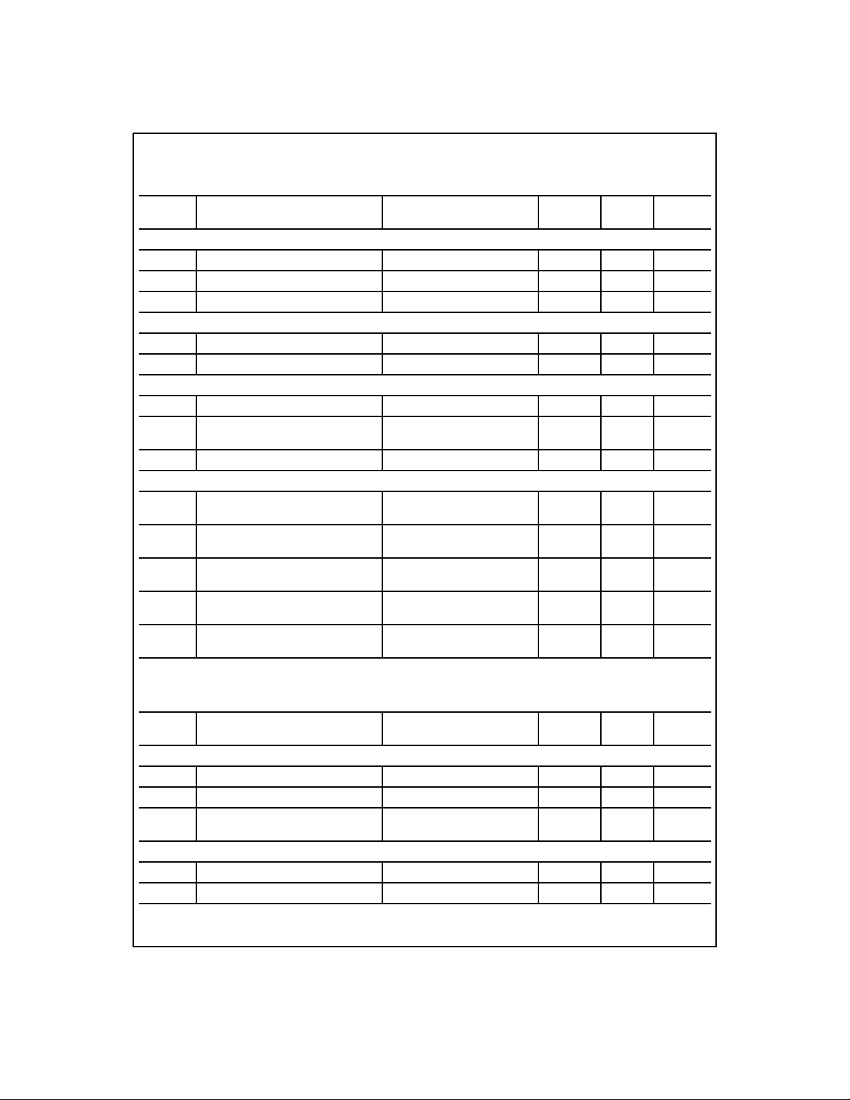
LM9810 Electrical Characteristics
(
)
(
)
(
)
(
)
(
)
(
)
The following specifications apply for
T
A=TJ=TMIN
to T
; all other limits TA=TJ=25°C. All LSB limits are in units of the LM9810’s 10 bit ADC.
MAX
AGND=DGND
=0V, VA=VD=+5.0V
Symbol Parameter Conditions
ADC Characteristics
Resolution with No Missing Codes 10 bits (min)
INL Integral Non-Linearity Error
(Note 11)
DNL Differential Non-Linearity ±0.25 ±1.0 LSB (max)
Full Channel Linearity
INL Integral Non-Linearity Error
Note 14
(Note 11)
DNL Differential Non-Linearity ±0.40 LSB
Static Offset DAC Characteristics
Monotonicity 6 bits (min)
Offset DAC LSB size PGA gain = 1 5
Offset DAC Adjustment Range PGA gain = 1 ±150 ±140 LSB (min)
System Characteristics (see section 1.7.1, Internal Offsets)
Analog Channel Gain Constant
C
(ADC Codes/V)
V
V
V
V
Pre-Boost Analog Channel Offset Error,
OS1
CCD Mode
Pre-Boost Analog Channel Offset Error,
OS1
CIS Mode
Pre-PGA Analog Channel Offset Error -10
OS2
Post-PGA Analog Channel Offset Error -11
OS3
Includes voltage reference
variation, gain setting = 1
, f
=24MHz, Rs=25Ω. Boldface limits apply for
DC
MCLK
(Notes 7, 8, & 12)
Typical
Note 9
±0.35 ±1.5 LSB (max)
±0.9 LSB
502
4.4
4.5
Limits
Note 10
3.4
6.4
468
532
-7.2
+15.7
-6.5
+15.2
-28
+5.3
-30.6
+7.3
LSB (min)
LSB (max)
LSB (min)
LSB (max)
LSB (min)
LSB (max)
LSB (min)
LSB (max)
LSB (min)
LSB (max)
LSB (min)
LSB (max)
Units
(Limits)
LM9820 Electrical Characteristics
The following specifications apply for
T
A=TJ=TMIN
to T
; all other limits TA=TJ=25°C. All LSB limits are in units of the LM9820’s 12 bit ADC.
MAX
AGND=DGND
=0V, VA=VD=+5.0V
Symbol Parameter Conditions
ADC Characteristics
Resolution with No Missing Codes 12 bits (min)
INL Integral Non-Linearity Error
(Note 11)
DNL Differential Non-Linearity ±0.6
Full Channel Linearity
INL Integral Non-Linearity Error
Note 14
(Note 11)
DNL Differential Non-Linearity ±0.65 LSB
, f
=24MHz, Rs=25Ω. Boldface limits apply for
DC
MCLK
(Notes 7, 8, & 12)
Typical
Note 9
Limits
Note 10
±1.1 ±4.0 LSB (max)
+1.75
-1.0
±3.4 LSB
4
http://www.national.com
Units
(Limits)
LSB (max)
(
)
(
)
(
)
(
)
)
)
)
)
LM9820 Electrical Characteristics
The following specifications apply for
T
A=TJ=TMIN
to T
; all other limits TA=TJ=25°C. All LSB limits are in units of the LM9820’s 12 bit ADC.
MAX
AGND=DGND
(Continued)
=0V, VA=VD=+5.0V
,
f
DC
MCLK
Symbol Parameter Conditions
Static Offset DAC Characteristics
Monotonicity
Offset DAC LSB size PGA gain = 1 20
Offset DAC Adjustment Range PGA gain = 1 ±590
System Characteristics (see section 1.7.1, Internal Offsets)
Analog Channel Gain Constant
C
(ADC Codes/V)
V
V
V
V
Pre-Boost Analog Channel Offset Error,
OS1
CCD Mode
Pre-Boost Analog Channel Offset Error,
OS1
CIS Mode
Pre-PGA Analog Channel Offset Error -40
OS2
Post-PGA Analog Channel Offset Error -44
OS3
Includes voltage reference
variation, gain setting = 1
DC and Logic Electrical Characteristics
The following specifications apply for
T
A=TJ=TMIN
to T
; all other limits TA=TJ=25°C.
MAX
AGND=DGND
=0V, VA=VD=+5.0V
(Notes 7 & 8)
Symbol Parameter Conditions
D0-D2, MCLK, NewLine, SampCLK Digital Input Characteristics
V
V
C
Logical “1” Input Voltage
IN(1
Logical “0” Input Voltage
IN(0
I
Input Leakage Current
IN
Input Capacitance 5 pF
IN
VD
VD
V
IN
VIN=
=5.25V
=4.75V
=
D0-D5 Digital Output Characteristics
VD
V
V
OUT(1
OUT(0
I
OUT
Logical “1” Output Voltage
Logical “0” Output Voltage
TRI-STATE® Output Current
D0-D5
(
only)
=4.75V, I
VD
=4.75V, I
VD
=5.25V, I
V
OUT
V
OUT
Power Supply Characteristics
Operating
Analog Supply Current
I
A
Standby with input clocks stopped
Standby with input clocks running
Operating
Digital Supply Current
I
D
(Note 15)
Standby with input clocks stopped
Standby with input clocks running
VD
DGND
DGND
=
VD
=
DC
OUT
OUT
OUT
,
f
MCLK
=-360µA
=-10µA
=1.6mA
=24MHz, Rs=25Ω.
=24MHz, Rs=25Ω.
Boldface limits apply for
(Notes 7, 8, & 12)
Typical
Note 9
Limits
Note 10
6
14
26
±575
2008
17.6
18
1873
2129
-32.1
+68.9
-22.2
+57
-94.3
+16.4
-121
+28
Boldface limits apply for
Typical
Note 9
Limits
Note 10
2.0
0.8
0.1
-0.1
2.4
4.4
0.4
0.1
-0.1
45
0.8
57
0.9
3.0
220
110
320
200
220
Units
(Limits)
bits (min)
LSB (min)
LSB (max)
LSB (min)
LSB (min)
LSB (max)
LSB (min)
LSB (max)
LSB (min)
LSB (max)
LSB (min)
LSB (max)
LSB (min)
LSB (max)
Units
(Limits)
V (max)
V (min)
µA(max)
µA(max)
V (min)
V (min)
V (max)
µA
µA
mA (max)
mA (max)
mA
µA (max)
µA (max)
µA
5
http://www.national.com
AC Electrical Characteristics
The following specifications apply for
limits apply for T
A=TJ=TMIN
Symbol Parameter Conditions
AGND=DGND
to T
; all other limits TA=TJ=25°C.
MAX
=0V, VA=VD=+5.0V
(Notes 7 & 8)
=24MHz
,
t
MCLK
Typical
(Note 9)
=1/f
CLK
M
,
=5ns, Rs=25Ω.
t
r=tf
Limits
(Note 10)
,
f
DC
MCLK
Boldface
Units
(Limits)
f
MCLK
t
MCLK
t
SCNL
t
SampCLK
t
SampLo
t
SampHi
t
SampSU
t
DDO
t
HDO
t
SCLK
t
DSU
t
DH
t
SCLKLA
t
LASCLK
t
LA
t
LANL
Maximum
MCLK
MCLK
SampCLK
MCLK
Frequency
Duty Cycle
period 41 ns (min)
falling edge before
NewLine
falling edge
SampCLK
period
Low time for
High time for
SampCLK
edge of
falling edge of
SampCLK
SampCLK
falling edge before rising
MCLK
MCLK
before new valid
50 ns (min)
50 ns (min)
data
hold time of current data from falling
MCLK
edge of
D2
(SCLK) Serial Clock Period 1 t
Input data setup time before
D2
(SCLK) rising edge
Input data hold time after D2(SCLK)
rising edge
D2
(SCLK) rising edge after bit B0
D1
before
(Latch) rising edge
D1
(Latch) rising edge before next
D2
(SCLK) rising edge
High time for D1(Latch)
D1
(Latch) rising edge before
NewLine
falling edge
24
40
60
3
4
4
40
15
0
3
3
3
3
3
MHz (min)
% (min)
% (max)
t
(min)
MCLK
t
(min)
MCLK
ns (min)
ns (max)
ns (min)
(min)
MCLK
ns (min)
ns (min)
ns (min)
ns (min)
t
(min)
MCLK
t
SampCLK
(min)
Note 1: Absolute Max im um R atings indicate limits beyond wh ic h damage to the device may occur. Operating R atings indicate condit ions for which the device is functional,
but do not guarantee specific perfor m ance limits. For guaranteed specifications an d test conditions, see the Electrical C haracteristics. The guaranteed specifications apply
only for the test condition s lis te d. Some performance ch arac t eristics may degrade when th e devi ce is not operated under the listed te s t conditions.
Note 2: All voltages are measured with respect to GND=
Note 3: When the input voltage (V
maximum package inp ut c urrent rating limits the num ber of pins that can simultan eously safely exceed the power suppli es w it h an input current of 25mA t o two.
Note 4: The maximum power dissipation must be derated at elevated temperatures and is dictated by T
able power dissipation at any temperature is P
is 84°C/W for the M20B SOI C package
Note 5: Human body m odel, 100pF capacit or discharged through a 1. 5kΩ resistor.
Note 6: See AN450 “Surface M ount ing M et hods and T heir Effect o n Prod uct Re liabilit y” o r the sect ion ti tled “ Surface M oun t” found in any N ation al Se mic ondu cto r Linea r
Data Book for other methods of soldering surface mount devices.
) at any pin exceed s the p ower su ppl ies (VIN<GND or VIN>VA or VD), the current at that pin sho uld be limite d to 25mA . The 50mA
IN
.
AGND=DGND
= (TJmax - TA) / ΘJA. TJmax = 150°C for this device. The typical thermal resistance (ΘJA) of this part when board moun te d
D
=0V, unless otherwise specified.
6
max, ΘJA and the ambient temperatu re, TA. The maximum a llow -
J
http://www.national.com
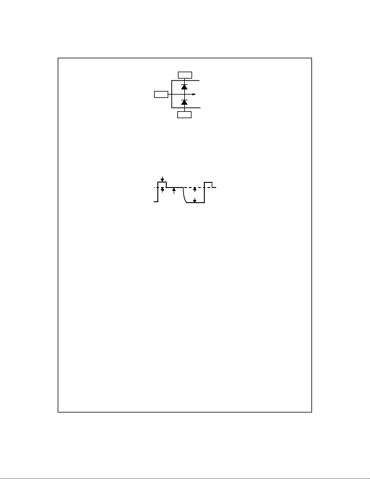
Note 7: Two diodes clamp the OS analo g inputs to
impedance of the sens or, prevents damage to the LM9810/2 0 f rom t ransients during power-u p.
AGND
and VA as shown below. This input protection, in co m bination with the external clamp capa c it or and the output
VA
OS Input
TO INTERNAL
CIRCUITRY
AGND
Note 8: To guarantee accuracy, it is required that VA and VD be connected together to the same power supply with separate bypass capacitors at each supply pin.
Note 9: Typicals are at T
J=TA
=25°C, f
= 24MHz, and repre s ent most likely parametric norm.
MCLK
Note 10: Tested limits are guaranteed to Nat ional's AOQL (Average Outgoing Quali ty Level).
Note 11: Integral non-linearity error is defined as the deviation of the analog value, expressed in LSBs, from the straight line th at best fits the actual transfer function of the
ADC.
Note 12: V
a white (full scale) image with respect to the reference level, V
correctable range of pixel-to-pixel V
LM9810/20 can corr ec t for using its internal PGA .
Note 13: PGA Gain Error is the maximum difference between the measured gain for any PGA code and the ideal gain calculated by using the formula
Gain
is defined as the CCD OS voltage for the reference period f ollowing the reset feedthrough pulse. V
PGA
REF
V
--- -
V
variation is define d as the maximu m variation in V
WHITE
PGA code
G0X
where .
-------------- ------------ -+=XG
32
31G0
.
REF
32
–()
------=
31
V
is defined as the peak positive deviation above V
RFT
CCD Output Signal
V
RFT
V
V
REF
WHITE
(due to PRNU, light source intensity variation, optics, etc.) that the
WHITE
is defined as the peak CCD pixel output voltage for
WHITE
of the reset feedthrough pulse. The maximum
REF
Note 14: Full C hannel INL and DNL are tested with CDS disabled, negative signal polarity, and a single OS input with a gain register setting of 1 (000001b) and an offset
register setting of 0 (000000b).
Note 15: The digital supply current (I
The current required to switch the digital data bus can be calculated from: Isw = 2*Nd*Psw*CL*
of each data bit switchin g, C L is t he capacitive loading on each data pin,
6, Psw should be .5, and
ital output pin (
will be drawn through the
VD
D5
- D0) is 20pF and the period of tSampCLK is 1/6MHz or 167ns , then the digital switching current would be 7.2mA. The calculated digital switching current
VD
) does not include the load, data and switching frequency dependent current required to drive the digital output bus on pins (D5 - D0).
D
VD
is the digital suppl y volta ge and tSampCLK i s the period of the
VD
/tSampCLK where N d is total number of data pins, Psw is the probability
SampCLK
signal. Since Nd is
is nominally 5V, the switching current can usually be calculated from: Isw = 30*CL/tSampCLK. For example, if the capacitive load on each dig-
pin and should be con s idered as part of the total power budget for he LM9810/20.
7
http://www.national.com
 Loading...