

NSC LM7915MWC, LM7915CK, LM7912MWC, LM7912MDC, LM7912CK Datasheet
...
LM79XX Series
3-Terminal Negative Regulators
General Description
The LM79XX series of 3-terminal regulators is available with
fixed output voltagesof−5V, −12V,and −15V. These devices
need only one external component —a compensation capacitor at the output. The LM79XX series is packaged in the
TO-220 power package and is capable of supplying 1.5A of
output current.
These regulators employ internal current limiting safe area
protection and thermal shutdown for protection against virtually all overload conditions.
Low ground pin current of the LM79XX series allows output
voltage to be easily boosted above the preset value with a
resistor divider. The low quiescent current drain of these
devices with a specified maximum change with line and load
ensures good regulation in the voltage boosted mode.
For applications requiring other voltages, see LM137
datasheet.
Features
n Thermal, short circuit and safe area protection
n High ripple rejection
n 1.5A output current
n 4% tolerance on preset output voltage
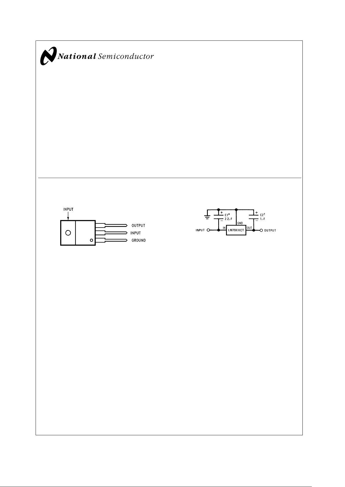
Connection Diagrams Typical Applications
*
Required if regulator is separated from filter capacitor by
more than 3". For value given, capacitor must be solid
tantalum. 25µF aluminum electrolytic may be substituted.
†
Required for stability. For value given, capacitor must be
solid tantalum. 25µF aluminum electrolytic may be substituted. Values given may be increased without limit.
For output capacitance in excess of 100µF, a high current
diode from input to output (1N4001, etc.) will protect the
regulator from momentary input shorts.
TO-220 Package
DS007340-14
Front View
Order Number LM7905CT, LM7912CT or LM7915CT
See NS Package Number TO3B
Fixed Regulator
DS007340-3
September 2001
LM79XX Series 3-Terminal Negative Regulators
© 2001 National Semiconductor Corporation DS007340 www.national.com
Absolute Maximum Ratings (Note 1)
If Military/Aerospace specified devices are required,
please contact the National Semiconductor Sales Office/
Distributors for availability and specifications.
Input Voltage
(V
o
= −5V) −25V
(V
o
= −12V and −15V) −35V
Input-Output Differential
(V
o
= −5V) 25V
(V
o
= −12V and −15V) 30V
Power Dissipation (Note 2) Internally Limited
Operating Junction Temperature Range 0˚C to +125˚C
Storage Temperature Range −65˚C to +150˚C
Lead Temperature (Soldering, 10 sec.) 230˚C
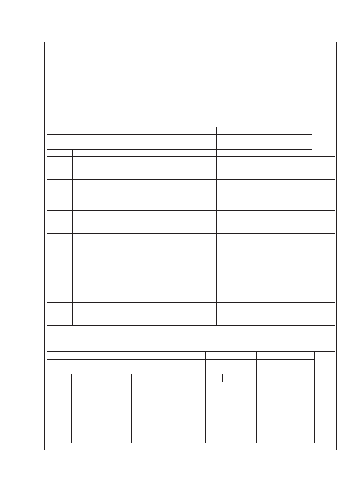
Electrical Characteristics
Conditions unless otherwise noted: I
OUT
= 500mA, CIN= 2.2µF, C
OUT
= 1µF, 0˚C ≤ TJ≤ +125˚C, Power Dissipation ≤ 1.5W.
Part Number LM7905C Units
Output Voltage −5V
Input Voltage (unless otherwise specified) −10V
Symbol Parameter Conditions Min Typ Max
V
O
Output Voltage TJ= 25˚C −4.8 −5.0 −5.2 V
5mA ≤ I
OUT
≤ 1A, −4.75 −5.25 V
P ≤ 15W (−20 ≤ V
IN
≤ −7) V
∆V
O
Line Regulation TJ= 25˚C, (Note 3) 8 50 mV
(−25 ≤ V
IN
≤ −7) V
215mV
(−12 ≤ V
IN
≤ −8) V
∆V
O
Load Regulation TJ= 25˚C, (Note 3)
5mA ≤ I
OUT
≤ 1.5A 15 100 mV
250mA ≤ I
OUT
≤ 750mA 5 50 mV
I
Q
Quiescent Current TJ= 25˚C 1 2 mA
∆I
Q
Quiescent Current With Line 0.5 mA
Change (−25 ≤ V
IN
≤ −7) V
With Load, 5mA ≤ I
OUT
≤ 1A 0.5 mA
V
n
Output Noise Voltage TA= 25˚C, 10Hz ≤ f ≤ 100Hz 125 µV
Ripple Rejection f = 120Hz 54 66 dB
(−18 ≤ V
IN
≤ −8) V
Dropout Voltage T
J
= 25˚C, I
OUT
= 1A 1.1 V
I
OMAX
Peak Output Current TJ= 25˚C 2.2 A
Average Temperature I
OUT
= 5mA, 0.4 mV/˚C
Coefficient of 0 C ≤ T
J
≤ 100˚C
Output Voltage
Electrical Characteristics
Conditions unless otherwise noted: I
OUT
= 500mA, CIN= 2.2µF, C
OUT
= 1µF, 0˚C ≤ TJ≤ +125˚C, Power Dissipation ≤ 1.5W.
Part Number LM7912C LM7915C Units
Output Voltage −12V −15V
Input Voltage (unless otherwise specified) −19V −23V
Symbol Parameter Conditions Min Typ Max Min Typ Max
V
O
Output Voltage TJ= 25˚C −11.5 −12.0 −12.5 −14.4 −15.0 −15.6 V
5mA ≤ I
OUT
≤ 1A, −11.4 −12.6 −14.25 −15.75 V
P ≤ 15W (−27 ≤ V
IN
≤ −14.5) (−30 ≤ VIN≤ −17.5) V
∆V
O
Line Regulation TJ= 25˚C, (Note 3) 5 80 5 100 mV
(−30 ≤ V
IN
≤ −14.5) (−30 ≤ VIN≤ −17.5) V
3 30 3 50 mV
(−22 ≤ V
IN
≤ −16) (−26 ≤ VIN≤−20) V
∆V
O
Load Regulation TJ= 25˚C, (Note 3)
LM79XX Series
www.national.com 2
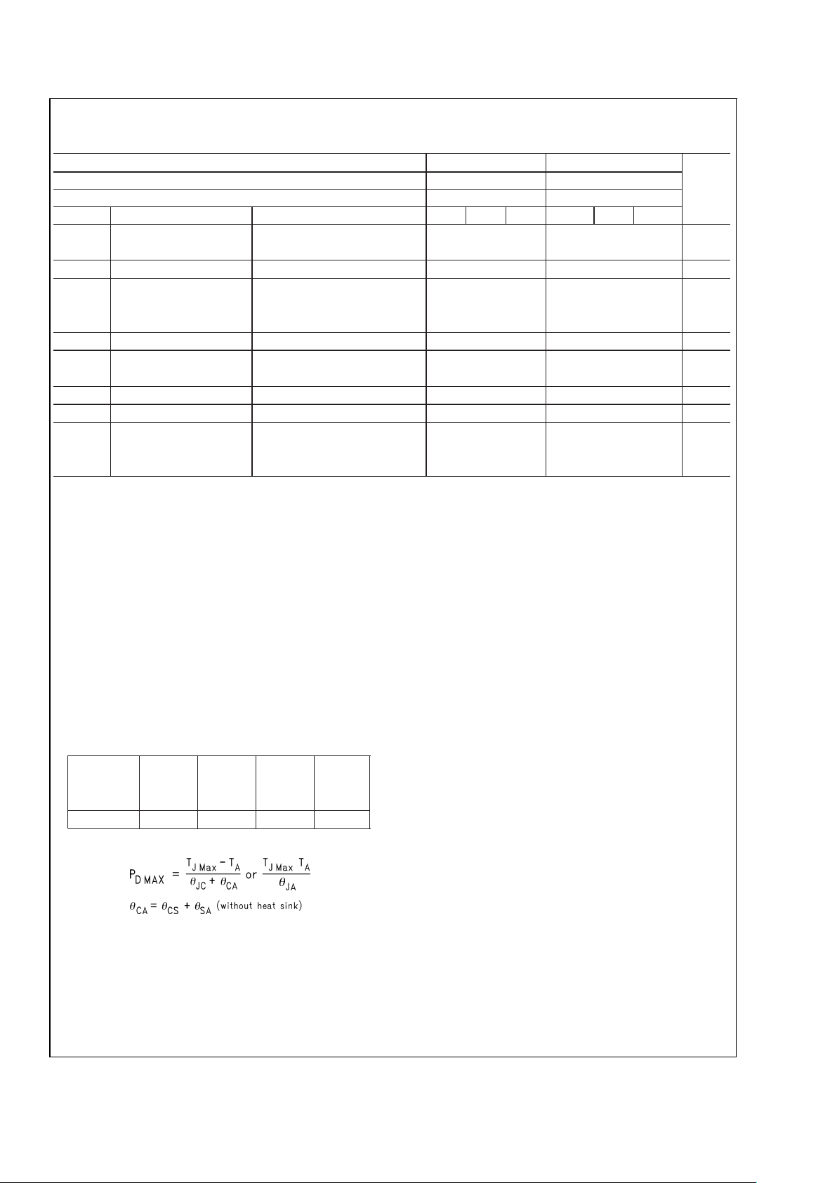
Electrical Characteristics (Continued)
Conditions unless otherwise noted: I
OUT
= 500mA, CIN= 2.2µF, C
OUT
= 1µF, 0˚C ≤ TJ≤ +125˚C, Power Dissipation ≤ 1.5W.
Part Number LM7912C LM7915C Units
Output Voltage −12V −15V
Input Voltage (unless otherwise specified) −19V −23V
Symbol Parameter Conditions Min Typ Max Min Typ Max
5mA ≤ I
OUT
≤ 1.5A 15 200 15 200 mV
250mA ≤ I
OUT
≤ 750mA 5 75 5 75 mV
I
Q
Quiescent Current TJ= 25˚C 1.5 3 1.5 3 mA
∆I
Q
Quiescent Current With Line 0.5 0.5 mA
Change (−30 ≤ V
IN
≤ −14.5) (−30 ≤VIN≤ −17.5) V
With Load, 5mA ≤ I
OUT
≤ 1A 0.5 0.5 mA
V
n
Output Noise Voltage TA= 25˚C, 10Hz ≤ f ≤ 100Hz 300 375 µV
Ripple Rejection f = 120 Hz 54 70 54 70 dB
(−25 ≤ V
IN
≤ −15) (−30 ≤ VIN≤ −17.5) V
Dropout Voltage T
J
= 25˚C, I
OUT
= 1A 1.1 1.1 V
I
OMAX
Peak Output Current TJ= 25˚C 2.2 2.2 A
Average Temperature I
OUT
= 5mA, −0.8 −1.0 mV/˚C
Coefficient of 0 C ≤ T
J
≤ 100˚C
Output Voltage
Note 1: Absolute Maximum Ratings indicate limits beyond which damage to the device may occur. Operating Ratings indicate conditions for which the device is
intended to be functional, but do not guarantee Specific Performance limits. For guaranteed specifications and test conditions, see the Electrical Characteristics.
Note 2: Refer to Typical Performance Characteristics and Design Considerations for details.
Note 3: Regulation is measured at a constant junction temperature by pulse testing with a low duty cycle. Changes in output voltage due to heating effects must
be taken into account.
Design Considerations
The LM79XX fixed voltage regulator series has thermal
overload protection from excessive power dissipation, internal short circuit protection which limits the circuit’s maximum
current, and output transistor safe-area compensation for
reducing the output current as the voltage across the pass
transistor is increased.
Although the internal power dissipation is limited, the junction temperature must be kept below the maximum specified
temperature (125˚C) in order to meet data sheet specifications. To calculate the maximum junction temperature or
heat sink required, the following thermal resistance values
should be used:
Typ Max Typ Max
Package θ
JC
θ
JC
θ
JA
θ
JA
˚C/W ˚C/W ˚C/W ˚C/W
TO-220 3.0 5.0 60 40
Solving for TJ:
T
J=TA+PD(θJC
+ θCA)or
=T
A+PDθJA
(without heat sink)
Where:
T
J
= Junction Temperature
T
A
= Ambient Temperature
P
D
= Power Dissipation
θ
JA
= Junction-to-Ambient Thermal Resistance
θ
JC
= Junction-to-Case Thermal Resistance
θ
CA
= Case-to-Ambient Thermal Resistance
θ
CS
= Case-to-Heat Sink Thermal Resistance
θ
SA
= Heat Sink-to-Ambient Thermal Resistance
LM79XX Series
www.national.com3
 Loading...