

NSC LM78MGCP, LM78M08CT, LM78GCP, LM78CCVFX, LM78M08CH Datasheet
...
LM78
Microprocessor System Hardware Monitor
General Description
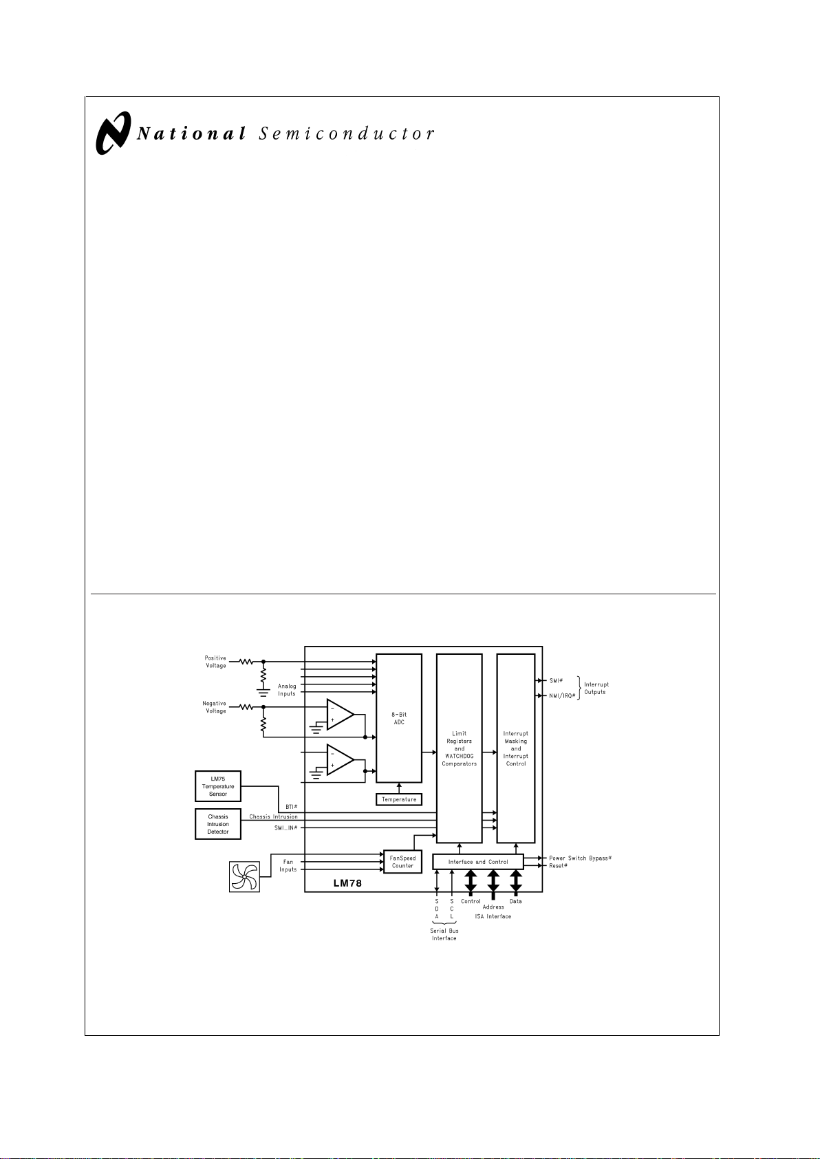
The LM78 is a highly integrated Data Acquisition system for
hardware monitoring of servers, Personal Computers, or
virtually any microprocessor based system. In a PC, the
LM78 can be used to monitor power supply voltages, temperatures, and fan speeds. Actual values for these inputs
can be read at any time, and programmable WATCHDOG
limits in the LM78 activate a fully programmable and
maskable interrupt system with two outputs.
The LM78 has an on-chip temperature sensor, 5 positive
analog inputs, two inverting inputs (for monitoring negative
voltages), and an 8-bit ADC. An input is provided for the
overtemperature outputs of additional temperature sensors
and this is linked to the interrupt system. The LM78 provides
inputs for three fan tachometer outputs. Additional inputs are
provided for Chassis Intrusion detection circuits, VID monitor
inputs, and chainable interrupt. The LM78 provides both ISA
and Serial Bus interfaces. A 32-byte auto-increment RAM is
provided for POST (Power On Self Test) code storage.
Applications
n System Hardware Monitoring for Servers and PCs
n Office Electronics
n Electronic Test Equipment and Instrumentation
Features
n Temperature sensing
n 5 positive voltage inputs
n 2 op amps for negative voltage monitoring
n 3 fan speed monitoring inputs
n Input for additional temperature sensors
n Chassis Intrusion Detector input
n WATCHDOG comparison of all monitored values
n POST code storage RAM
n ISA and I
2
C™Serial Bus interfaces
Key Specifications
j
Voltage monitoring
accuracy
±
1% (max)
j
Temperature Accuracy
−10˚C to +100˚C
±
3˚C (max)
j
Supply Voltage 5V
j
Supply Current Operating: 1 mA typ
Shutdown: 10 µA typ
j
ADC Resolution 8 Bits
Typical Application
I2C®is a registered trademark of the Phillips Corporation.
DS012873-1
#
indicates Active Low (”Not“)
February 2000
LM78 Microprocessor System Hardware Monitor
© 2001 National Semiconductor Corporation DS012873 www.national.com
Ordering Information
Temperature Range
Package
−10˚C ≤ T
A
≤ +100˚C
Order Number Device Marking
LM78CCVF LM78CCVF-J VGZ44A
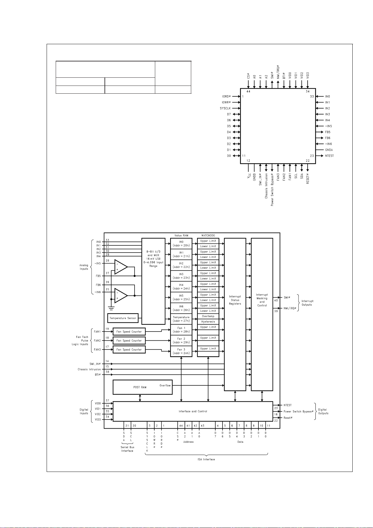
Connection Diagram
Block Diagram
DS012873-2
DS012873-3
LM78
www.national.com 2
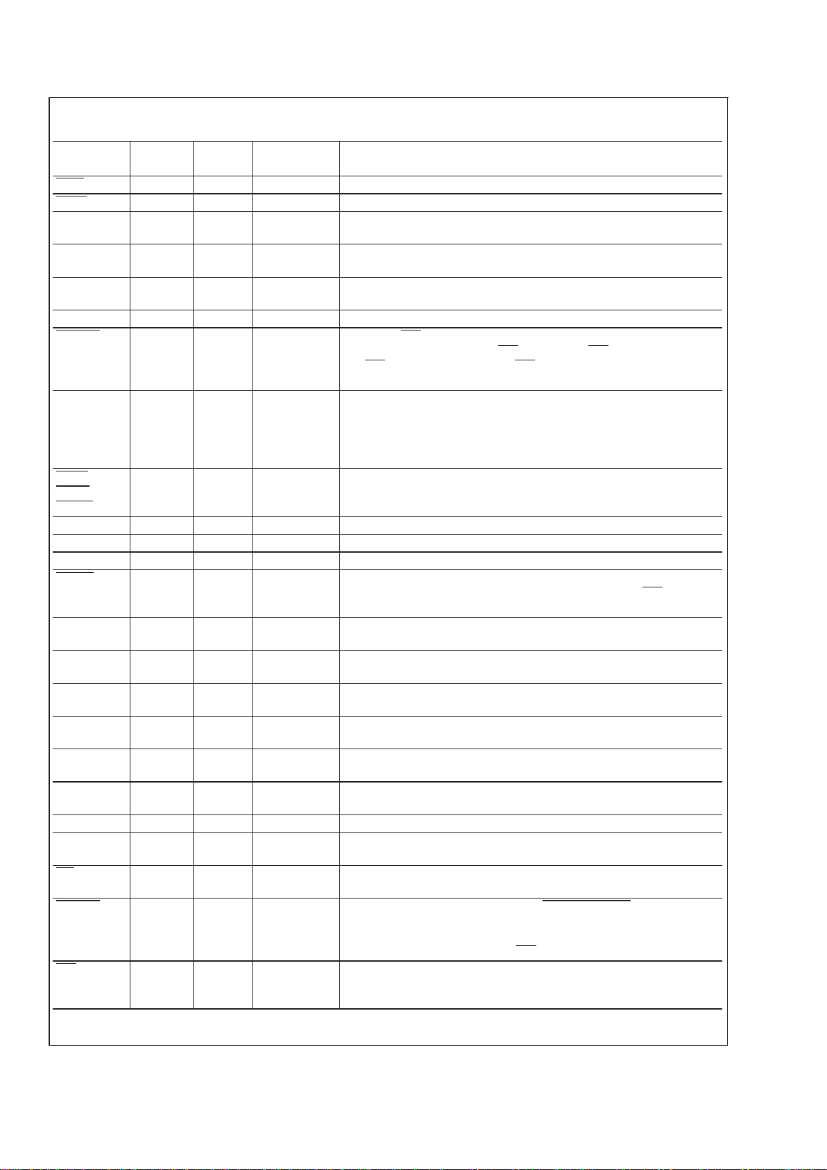
Pin Descriptions
Pin
Name(s)
Pin
Number
Number
of Pins
Type Description
IORD
1 1 Digital Input An active low standard ISA bus I/O Read Control.
IOWR
2 1 Digital Input An active low standard ISA bus I/O Write Control.
SYSCLK 3 1 Digital Input The reference clock for the ISA bus. Typically ranges from 4.167 MHz to
8.33 MHz. The minimum clock frequency this input can handle is 1 Hz.
D7–D0 4–11 8 Digital I/O Bi-directional ISA bus Data lines. D0 corresponds to the low order bit,
with D7 the high order bit.
V
CC
(+5V) 12 1 POWER +5V VCCpower. Bypass with the parallel combination of 10 µF
(electolytic or tantalum) and 0.1 µF (ceramic) bypass capacitors.
GNDD 13 1 GROUND Internally connected to all digital circuitry.
SMI__IN
14 1 Digital Input Chainable SMI (System Management Interrupt) Input. This is an active
low input that propagates the SMI signal to the SMI output of the LM78
via SMI Mask Register Bit 6 and SMI enable Bit 1 of the Configuration
Register.
Chassis
Intrusion
15 1 Digital I/O An active high input from an external circuit which latches a Chassis
Intrusion event. This line can go high without any clamping action
regardless of the powered state of the LM78. The LM78 provides an
internal open drain on this line, controlled by Bit 7 of NMI Mask Register
2, to provide a minimum 20 ms reset of this line.
Power
Switch
Bypass
16 1 Digital Output An active low push-pull output intended to drive an external P-channel
power MOSFET for software power control.
FAN3–FAN1 17–19 3 Digital Input 0V to +5V amplitude fan tachometer input.
SCL 20 1 Digital Input Serial Bus Clock.
SDA 21 1 Digital I/O Serial Bus bidirectional Data.
RESET
22 1 Digital Output Master Reset, 5 mA driver (open drain), active low output with a 20 ms
minimum pulse width. Available when enabeld via Bit 7 in SMI Mask
Register 2.
NTEST 23 1 Test Output NAND Tree totem-pole output that provides board-level connectivity
testing. Refer to Section 11.0 on NAND Tree testing.
GNDA 24 1 GROUND Internally connected to all analog circuitry. The ground reference for all
analog inputs.
−IN6 25 1 Analog Input Ground-referred inverting op amp input. Refer to Section 4.0, “ANALOG
INPUTS”.
FB6 26 1 Analog Output Output of inverting op amp for Input 6. Refer to section 4.0, “ANALOG
INPUTS”.
FB5 27 1 Analog Output Output of inverting op amp for Input 5. Refer to section 4.0, “ANALOG
INPUTS”.
−IN5 28 1 Analog Input Ground-referred inverting op amp input. Refer to Section 4.0, “ANALOG
INPUTS”.
IN4–IN0 29–33 5 Analog Input 0V to 4.096V FSR Analog Inputs.
VID3–VID0 34–37 4 Digital Input Voltage Supply readouts from P6. This value is read in the VID/Fan
Divisor Register.
BTI
38 1 Digital Input Board Temperature Interrupt driven by O.S. outputs of additional
temperature sensors such as LM75. Provides internal pull-up of 10 kΩ.
NMI/IRQ
39 1 Digital Output Non-Maskable Interrupt (open source)/Interrupt Request (open drain).
The mode is selected with Bit 5 of the Configuration Register and the
output is enabled when Bit 2 of the Configuration Register is set to 1.
The default state is disabled and IRQ mode.
SMI 40 1 Digital Output System Management Interrupt (open drain). This output is enabled when
Bit 1 in the Configuration Register is set to 1. The default state is
disabled.
LM78
www.national.com3
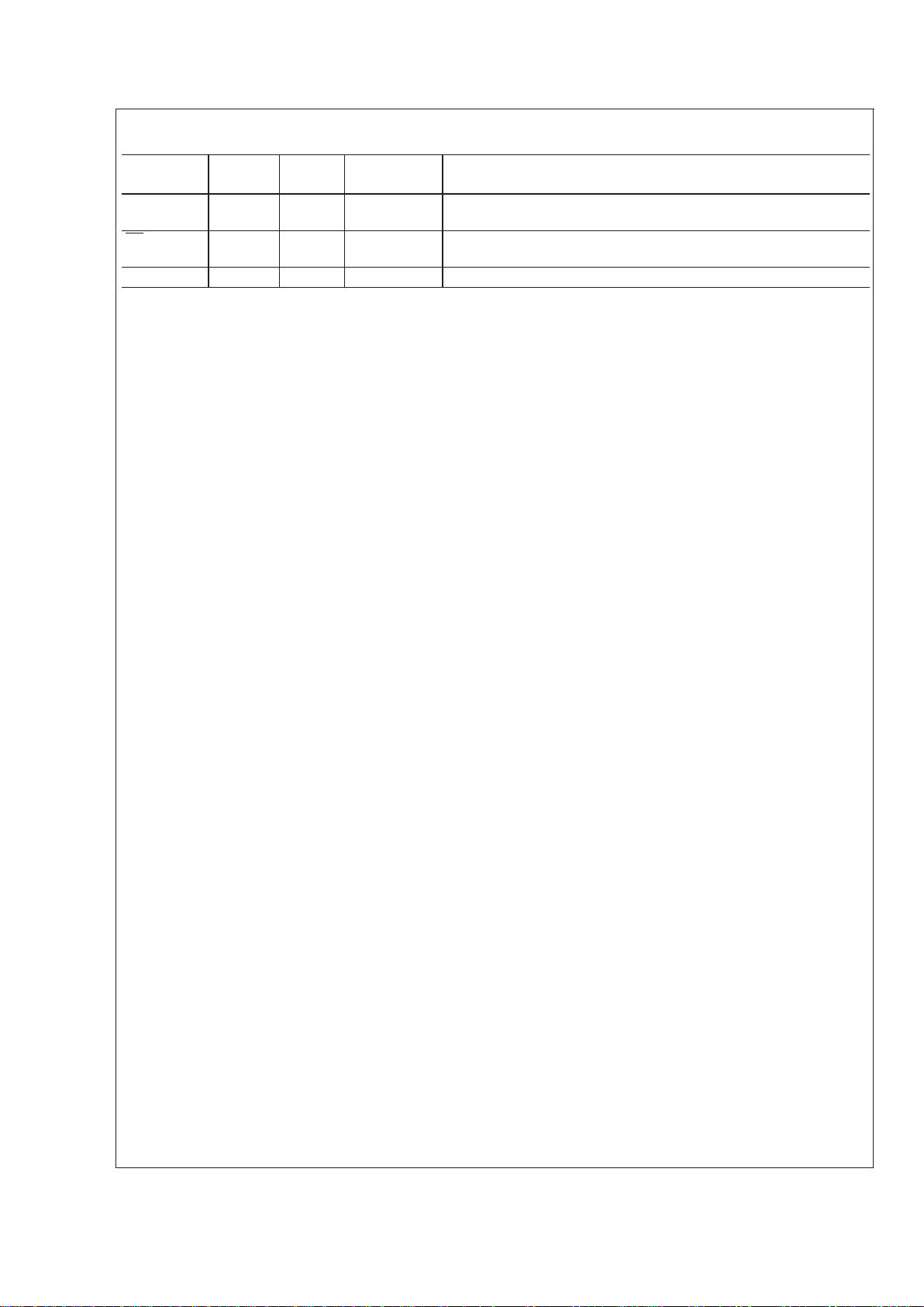
Pin Descriptions (Continued)
Pin
Name(s)
Pin
Number
Number
of Pins
Type Description
A2–A0 41–43 3 Digital Input The three lowest order bits of the 16-bit ISA Address Bus. A0
corresponds to the lowest order bit.
CS
44 1 Digital Input Chip Select input from an external decoder which decodes high order
address bits on the ISA Address Bus. This is an active low input.
TOTAL PINS 44
LM78
www.national.com 4
Absolute Maximum Ratings (Notes 1, 2)
If Military/Aerospace specified devices are required,
please contact the National Semiconductor Sales Office/
Distributors for availability and specifications.
Positive Supply Voltage (V
CC
) 6.5V
Voltage on Any Input or Output Pin −0.3V to (V
CC
+0.3V)
Ground Difference (GNDD–GNDA)
±
300 mV
Input Current at any Pin (Note 3)
±
5mA
Package Input Current (Note 3)
±
20 mA
Maximum Junction Temperature
(T
J
max) 150˚C
ESD Susceptibility(Note 5)
Human Body Model 2000V
Machine Model 175V
Soldering Information
PQFP Package (Note 6) :
Vapor Phase (60 seconds) 215˚C
Infrared (15 seconds) 220˚C
Storage Temperature −65˚C to +150˚C
Operating Ratings(Notes 1, 2)
Operating Temperature Range T
MIN
≤ TA≤ T
MAX
LM78 −55˚C ≤ TA≤ +125˚C
Specified Temperature Range T
MIN
≤ TA≤ T
MAX
LM78 −10˚C ≤ TA≤ +100˚C
Junction to Ambient Thermal Resistance (θ
JA
(Note 4) )
NS Package ID: VGZ44A 62˚C/W
Supply Voltage (V
CC
) +4.25V to +5.75V
Ground Difference
(IGNDD–GNDAI) ≤100 mV
V
IN
Voltage Range −0.05V to VCC+ 0.05V
DC Electrical Characteristics(Note 7)
The following specifications apply for +4.25 VDC≤VCC≤ +5.75 VDC,f
SYSCLK
= 8.33 MHz, RS=25Ω, unless otherwise speci-
fied. Boldface limits apply for T
A=TJ=TMIN
to T
MAX
; all other limits TA=TJ= 25˚C.
Symbol Parameter Conditions Typical Limits Units
(Note 8) (Note 9) (Limits)
POWER SUPPLY CHARACTERISTICS
I
CC
Supply Current Interface Inactive 1.0 2 mA (max)
Shutdown Mode 10 µA
TEMPERATURE-TO-DIGITAL CONVERTER CHARACTERISTICS
Accuracy −10˚C ≤ T
A
≤ +100˚C
±
3 ˚C (max)
Resolution 1 ˚C (min)
ANALOG-TO-DIGITAL CONVERTER CHARACTERISTICS
Resolution (8 bits with full-scale at 4.096V) 16 mV
TUE Total Unadjusted Error (Note 10)
±
1 % (max)
DNL Differential Non-Linearity
±
1 LSB
PSS Power Supply Sensitivity
±
1 %/V
t
C
Total Monitoring Cycle Time (Note 11) 1.0 1.5 sec (max)
OP AMP CHARACTERISTICS
Output Current (Sourcing) 50 µA
Input Offset Voltage I
OUT
=50µA
±
1mV
Input Bias Current
±
0.1 nA
PSRR 60 dB
DC Open Loop Gain 70 dB
Gain Bandwidth Product 500 kHz
MULTIPLEXER/ADC INPUT CHARACTERISTICS
On Resistance 400 2000 Ω (max)
Off Channel Leakage Current
±
0.1 nA
Input Current (On Channel Leakage Current)
±
0.1 nA
FAN RPM-TO-DIGITAL CONVERTER
Accuracy +25˚C ≤ T
A
≤ +75˚C
±
10 % (max)
−10˚C ≤ T
A
≤ +100˚C
±
15 % (max)
Full-scale Count 255 (max)
LM78
www.national.com5
DC Electrical Characteristics(Note 7) (Continued)
The following specifications apply for +4.25 VDC≤VCC≤ +5.75 VDC,f
SYSCLK
= 8.33 MHz, RS=25Ω, unless otherwise speci-
fied. Boldface limits apply for T
A=TJ=TMIN
to T
MAX
; all other limits TA=TJ= 25˚C.
Symbol Parameter Conditions Typical Limits Units
(Note 8) (Note 9) (Limits)
FAN RPM-TO-DIGITAL CONVERTER
FAN1 and FAN2 Nominal Input
RPM (See Section 6.0)
Divisor = 1, Fan Count = 153
(Note 12)
8800 RPM
Divisor = 2, Fan Count = 153
(Note 12)
4400 RPM
Divisor = 3, Fan Count = 153
(Note 12)
2200 RPM
Divisor = 4, Fan Count = 153
(Note 12)
1100 RPM
FAN3 Design Nominal Input RPM Fan Count = 153 (Note 12) 4400 RPM
Internal Clock Frequency +25˚C ≤ T
A
≤ +75˚C 22.5 20.2 kHz (min)
24.8 kHz (max)
−10˚C ≤ T
A
≤ +100˚C 22.5 19.1 kHz (min)
25.9 kHz (max)
DIGITAL OUTPUTS (Power Switch Bypass, NTEST, NMI/IRQ)
V
OUT(1)
Logical “1” Output Voltage I
OUT
=±5.0 mA 2.4 V (min)
V
OUT(0)
Logical “0” Output Voltage I
OUT
=±5.0 mA 0.4 V (max)
ISA D0–D7 DIGITAL OUTPUTS
V
OUT(1)
Logical “1” Output Voltage I
OUT
=±12.0 mA 2.4 V (min)
V
OUT(0)
Logical “0” Output Voltage I
OUT
=±12.0 mA 0.4 V (max)
I
OUT
TRI-STATE®Output Current V
OUT
=0V
DC
0.005 1 µA (max)
V
OUT
=V
CC
−0.005 −1 µA (min)
OPEN DRAIN DIGITAL OUTPUTS (SDA, RESET, SMI, Chassis Intrusion)
V
OUT(0)
Logical “0” Output Voltage I
OUT
= −5.0 mA 0.4 V (min)
I
OH
High Level Output Current V
OUT
=V
CC
0.1 100 µA (max)
RESET and Chassis Intrusion
45 20 ms (min)
Pulse Width
DIGITAL INPUTS: SMI__IN, VID0–VID3, BTI, CS, A0, A1, A2, Mode Control and Interface Inputs (IORD, IOWR, SYSCLK),
Data Lines (D0–D7), Chassis Intrusion, and Tach Pulse Logic Inputs (FAN1, FAN2, FAN3)
V
IN(1)
Logical “1” Input Voltage 2.0 V (min)
V
IN(0)
Logical “0” Input Voltage 0.8 V (max)
SERIAL BUS DIGITAL INPUTS (SCL, SDA)
V
IN(1)
Logical “1” Input Voltage 0.7xV
CC
V (min)
V
IN(0)
Logical “0” Input Voltage 0.3xV
CC
V (max)
ALL DIGITAL INPUTS EXCEPT FOR BTI
I
IN(1)
Logical “1” Input Current VIN=V
CC
−0.005 −1 µA (min)
I
IN(0)
Logical “0” Input Current VIN=0V
DC
0.005 1 µA (max)
C
IN
Digital Input Capacitance 20 pF
BIT DIGITAL INPUT
I
IN(1)
Logical “1” Input Current VIN=V
CC
1 10 µA (max)
I
IN(0)
Logical “0” Input Current VIN=0V
DC
−500 −2000 µA (max)
C
IN
Digital Input Capacitance 20 pF
LM78
www.national.com 6
AC Electrical Characteristics(Note 13) The following specifications apply for +4.25 V
DC
≤ VCC≤
+5.75 V
DC
unless otherwise specified. Boldface limits apply for TA=TJ=T
MIN
to T
MAX
; all other limits TA=TJ=
25˚C.
Symbol Parameter Conditions Typical Limits Units
(Note 8) (Note 9) (Limits)
ISA TIMING CHARACTERISTICS
f
SYSCLK
System Clock (SYSCLK) Input Frequency 8.33 MHz
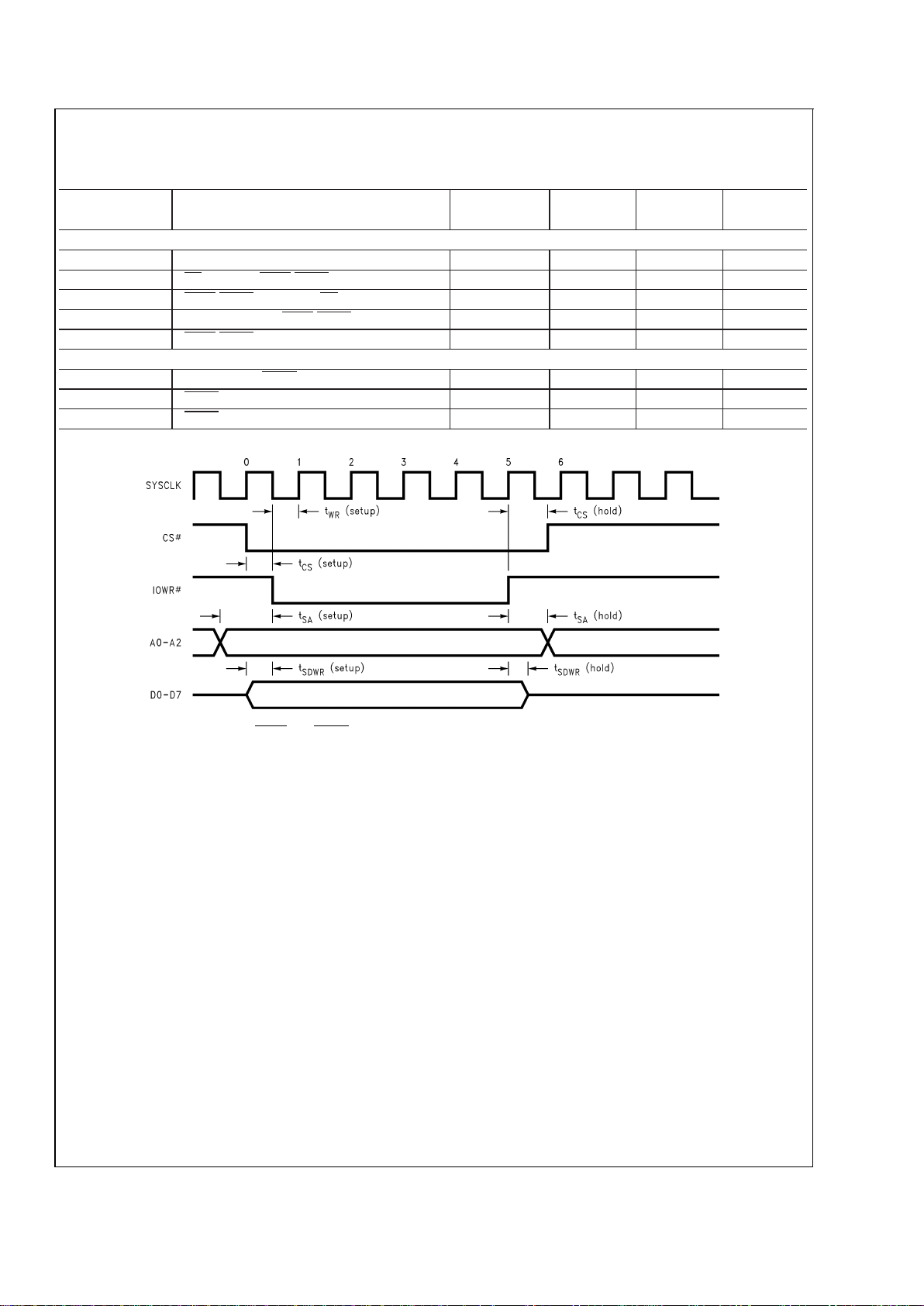
t
CS
(setup) CS Active to IORD/IOWR Active 10 ns (min)
t
CS
(hold) IORD/IOWR Inactive to CS Inactive 10 ns (min)
t
SA
(setup) Address Valid to IORD/IOWR Active 30 ns (min)
t
SA
(hold) IORD/IOWR Inactive to Address Invalid 10 ns (min)
ISA WRITE TIMING
t
SDWR
(setup) Data Valid to IOWR Active 5 ns (min)
t
SDWR
(hold) IOWR Inactive to Data Invalid 5 ns (min)
t
WR
(setup) IOWR Active to Rising Edge of SYSCLK 20 ns (min)
DS012873-4
The delay between consecutive IORD and IOWR pulses should be greater than 50 ns to ensure that an Power-on reset does not
occur unintentionally. (See Section 3.2 ‘Resets’ )
FIGURE 1. ISA Bus Write Timing Diagram
LM78
www.national.com7
AC Electrical Characteristics(Note 13) The following specifications apply for +4.25 V
DC
≤ VCC≤ +5.75 V
DC
unless otherwise specified. Boldface limits apply for TA=TJ=T
MIN
to T
MAX
; all other limits TA=TJ= 25˚C. (Continued)
Symbol Parameter Conditions Typical Limits Units
(Note 8) (Note 9) (Limits)
ISA READ TIMING
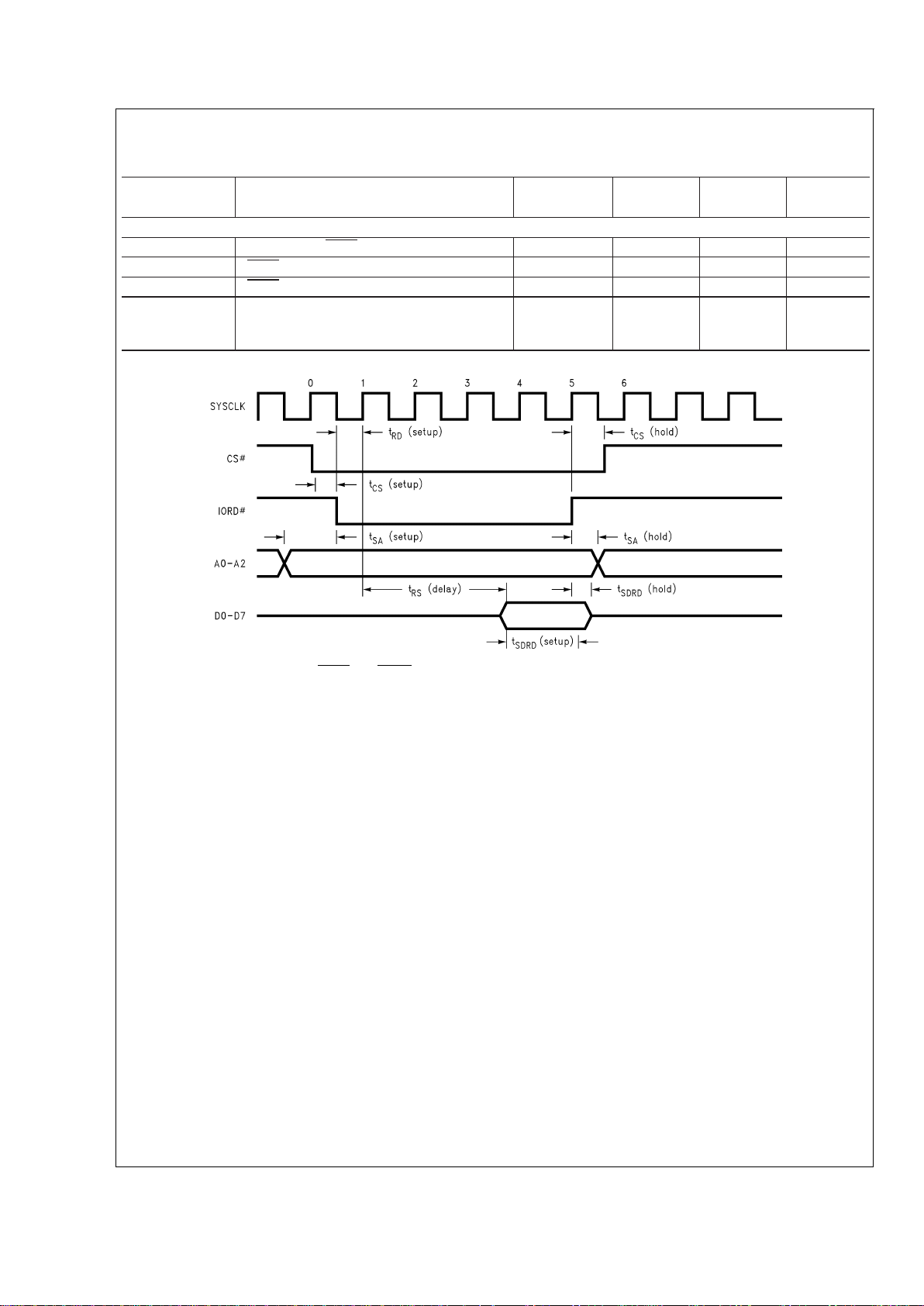
t
SDRD
(setup) Data Valid to IORD Inactive 120 ns (min)
t
SDRD
(hold) IORD Inactive to Data Invalid 5 ns (min)
t
RD
(setup) IORD Active to Rising Edge of SYSCLK 20 ns (min)
t
RS
(delay) Rising Edge of SYSCLK number 1 to Data
Valid
With 8.33
MHz
SYSCLK
360 ns (max)
DS012873-5
The delay between consecutive IORD and IOWR pulses should be greater than 50 ns to ensure that an Power-on reset does not
occur unintentionally. (SeeSection 3.2‘Resets’ )
FIGURE 2. ISA Bus Read Timing Diagram
LM78
www.national.com 8
AC Electrical Characteristics(Note 13) The following specifications apply for +4.25 V
DC
≤ VCC≤ +5.75 V
DC
unless otherwise specified. Boldface limits apply for TA=TJ=T
MIN
to T
MAX
; all other limits TA=TJ= 25˚C. (Continued)
Symbol Parameter Conditions Typical Limits Units
(Note 8) (Note 9) (Limits)
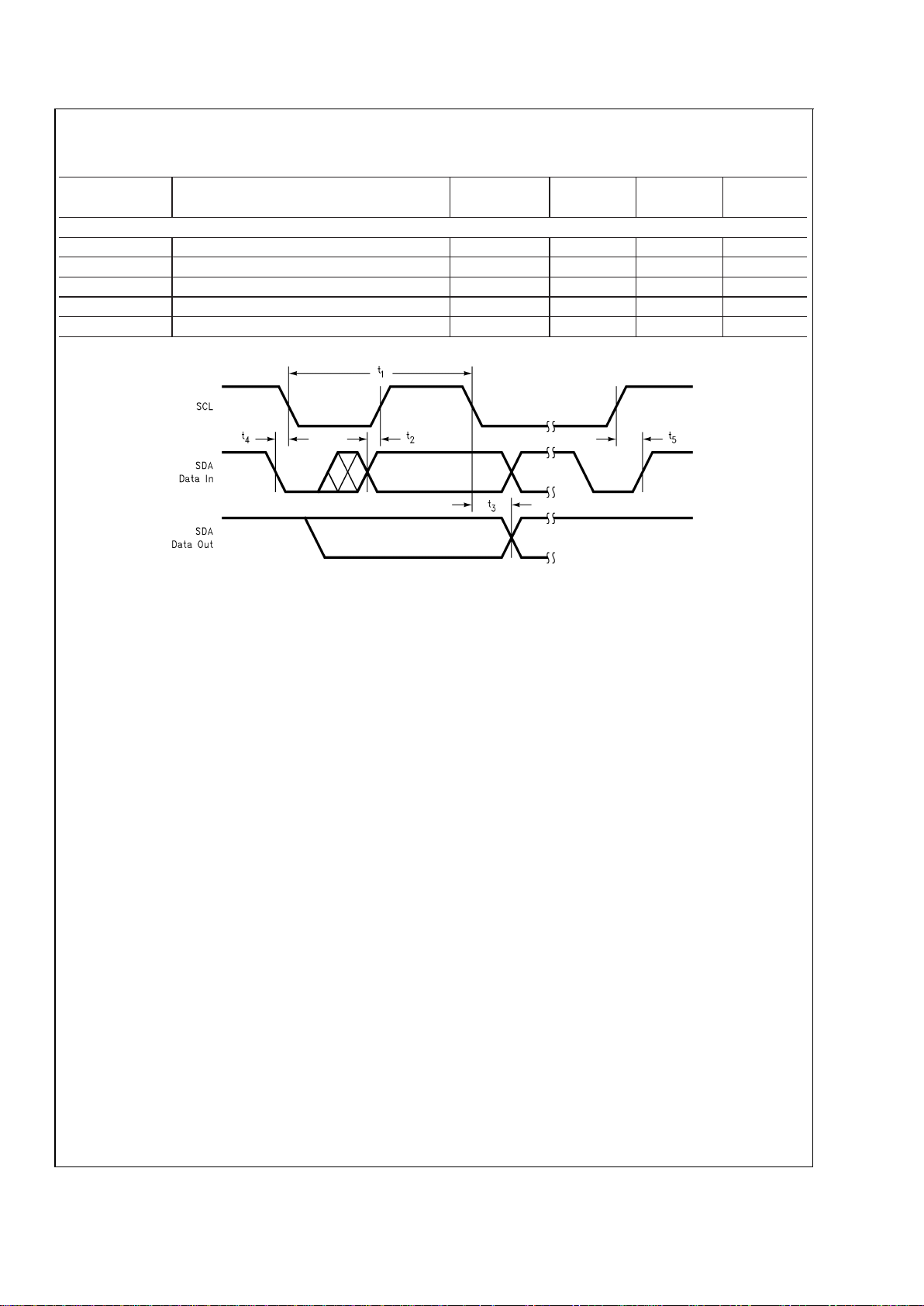
SERIAL BUS TIMING CHARACTERISTICS
t
1
SCL (Clock) Period 2.5 µs (min)
t
2
Data In Setup Time to SCL High 100 ns (min)
t
3
Data Out Stable After SCL Low 0 ns (min)
t
4
SDA Low Setup Time to SCL Low (start) 100 ns (min)
t
5
SDA High Hold Time After SCL High (stop) 100 ns (min)
DS012873-6
FIGURE 3. Serial Bus Timing Diagram
LM78
www.national.com9
Electrical Characteristics (Continued)
Note 1: Absolute Maximum Ratings indicate limits beyond which damage to the device may occur. Operating Ratings indicate conditions for which the device is
functional, but do not guarantee specific performance limits. For guaranteed specifications and test conditions, see the Electrical Characteristics. The guaranteed
specifications apply only for the test conditions listed. Some performance characteristics may degrade when the device is not operated under the listed test
conditions.
Note 2: All voltages are measured with respect to GND, unless otherwise specified
Note 3: When the input voltage (V
IN
) at any pin exceeds the power supplies (V
IN
<
(GNDD or GNDA) or V
IN
>
VCC), the current at that pin should be limited to 5 mA.
The 20 mA maximum package input current rating limits the number of pins that can safely exceed the power supplies with an input current of 5 mA to four.
Note 4: The maximum power dissipation must be derated at elevated temperatures and is dictated by T
J
max, θJAand the ambient temperature, TA. The maximum
allowable power dissipation at any temperature is P
D
=(TJmax−TA)/θJA.
Note 5: The human body model is a 100 pF capacitor discharged through a 1.5 kΩ resistor into each pin. The machine model is a 200 pF capacitor discharged
directly into each pin.
Note 6: See the section titled “Surface Mount” found in any post 1986 National Semiconductor Linear Data Book for other methods of soldering surface mount
devices.
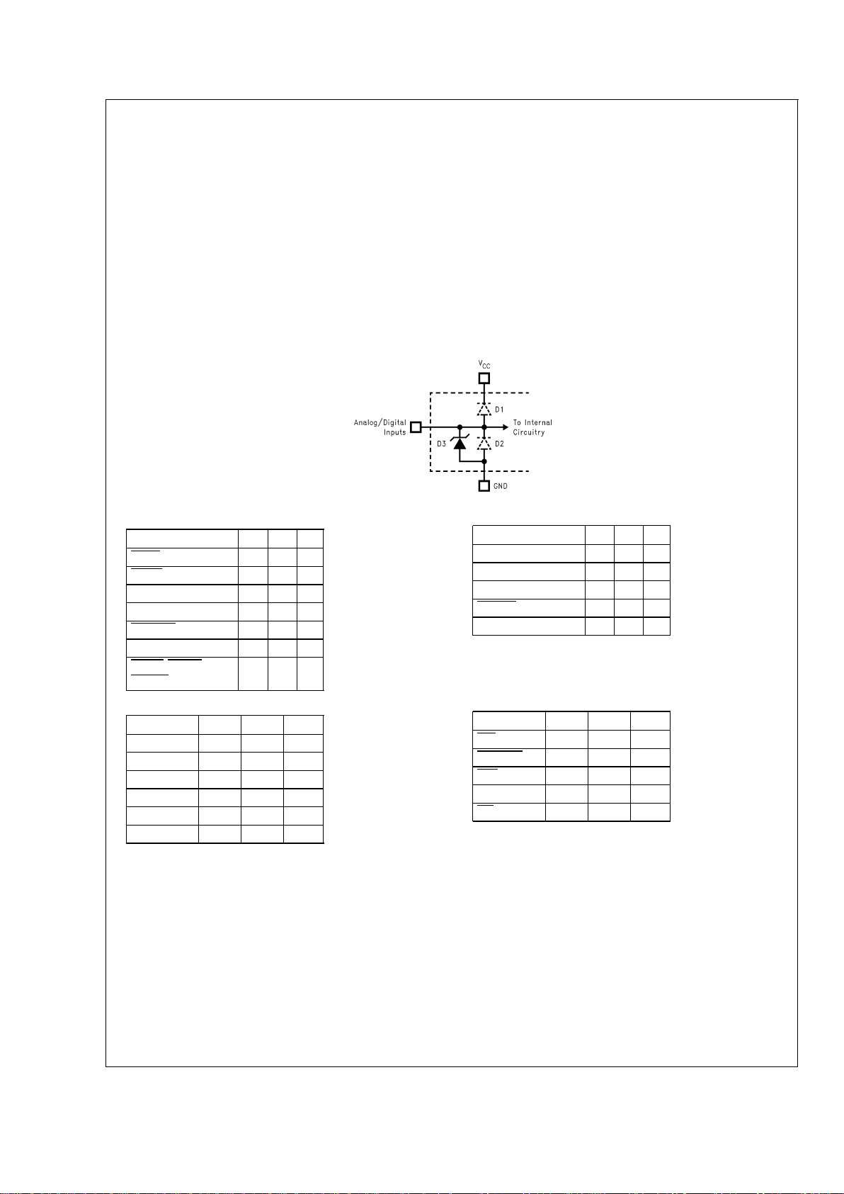
Note 7: Each input and output is protected by a nominal 6.5V breakdown voltage zener diode to GND; as shown below, input voltage magnitude up to 0.3V above
V
CC
or 0.3V below GND will not damage the LM78. There are parasitic diodes that exist between the inputs and the power supply rails. Errors in the ADC conversion
can occur if these diodes are forward biased by more than 50 mV. As an example, if V
CC
is 4.50 VDC, input voltage must be ≤ 4.55 VDC, to ensure accurate
conversions.
Note 8: Typicals are at T
J=TA
=25˚C and represent most likely parametric norm.
Note 9: Limits are guaranteed to National’s AOQL (Average Outgoing Quality Level).
Note 10: TUE (Total Unadjusted Error) includes Offset, Gain and Linearity errors of the ADC and any error introduced by the amplifiers as shown in the circuit of
Figure 13
.
Note 11: TotalMonitoring Cycle Time includes temperature conversion, 7 analog input voltage conversions and 3 tachometer readings. Each temperature and input
voltage conversion takes 100 ms typical and 112 ms maximum. Fan tachometer readings take 20 ms typical, at 4400 rpm, and 200 ms max.
Note 12: The total fan count is based on 2 pulses per revolution of the fan tachometer output.
Note 13: Timing specifications are tested at the TTL logic levels, V
IL
=0.4V for a falling edge and VIH=2.4V for a rising edge. TRI-STATE output voltage is forced
to 1.4V.
DS012873-7
An x indicates that the diode exists.
Pin Name D1 D2 D3
IORD
x
IOWR
x
SYSCLK x
D0–D7 xxx
SMI__IN
x
Chassis Intrusion x x
Power Switch
Bypass
xxx
Pin Name D1 D2 D3
FAN1–FAN3 x
SCL x
SDA x x
RESET
xx
NTEST x x x
Pin Name D1 D2 D3
−IN6 x x
FB6 x x x
FB5 x x x
−IN5 x x
IN4–IN0 x x x
VID3–VID0 x x x
Pin Name D1 D2 D3
BTI
xx
NMI/IRQ
xxx
SMI
xx
A0–A2 x
CS
x
FIGURE 4. ESD Protection Input Structure
LM78
www.national.com 10
 Loading...