

NSC LM77000CP, LM759CP, LM759CH, LM759MH, LM759H-883 Datasheet
LM759/LM77000
Power Operational Amplifiers
LM759/LM77000 Power Operational Amplifiers
November 1994
General Description
The LM759 and LM77000 are high performance operational
amplifiers that feature high output current capability. The
LM759 is capable of providing 325 mA and the LM77000
providing 250 mA. Both amplifiers feature small signal characteristics that are better than the LM741. The amplifiers
are designed to operate from a single or dual power supply
with an input common mode range that includes the negative supply. The high gain and high output power provide
superior performance. Internal current limiting, thermal shutdown, and safe area compensation are employed making
the LM759 and LM77000 essentially indestructible.
Features
Y
Output current
LM759Ð325 mA minimum
LM77000Ð250 mA minimum
Y
Internal short circuit current limiting
Y
Internal thermal overload protection
Y
Internal output transistors safe-area protection
Y
Input common mode voltage range includes ground or
negative supply
Applications
Y
Voltage regulators
Y
Audio amplifiers
Y
Servo amplifiers
Y
Power drivers
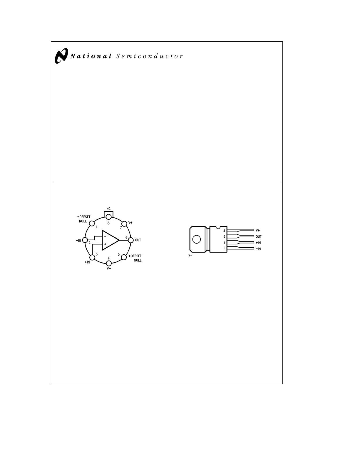
Connection Diagrams and Ordering Information
Lead 4 connected to case.
TL/H/10075– 1
Top View
Order Number LM759MH, LM759CH or LM759H/883
See NS Package Number H08C
Order Number LM759CP or LM77000CP
See NS Package Number P04A
Top View
TL/H/10075– 2
C
1995 National Semiconductor Corporation RRD-B30M115/Printed in U. S. A.
TL/H/10075
Absolute Maximum Ratings
If Military/Aerospace specified devices are required,
please contact the National Semiconductor Sales
Office/Distributors for availability and specifications.
Storage Temperature Range
Metal Can
Plastic Package
Operating Junction Temperature Range
Military (LM759M)
Commercial (LM759C, LM77000C) 0
b
65§Ctoa175§C
b
65§Ctoa150§C
b
55§Ctoa150§C
Ctoa125§C
§
Lead Temperature
Metal Can (soldering, 60 sec) 300
Plastic Package (soldering, 10 sec) 265
§
§
Internal Power Dissipation (Note 1) Internally Limited
Supply Voltage
Differential Input Voltage 30V
Input Voltage (note 2)
C
C
g
18V
g
15V
LM759
Electrical Characteristics
e
T
25§C, V
J
Symbol Parameter Conditions Min Typ Max Units
V
IO
I
IO
I
IB
Z
I
I
CC
V
IR
I
OS
I
O PEAK
A
VS
TR Transient Response Rise Time R
Input Offset Voltage R
S
Input Offset Current 5.0 30 nA
Input Bias Current 50 150 nA
Input Impedance 0.25 1.5 MX
Supply Current 12 18 mA
Input Voltage Range V
Output Short Circuit Current
VCC–V
l
Peak Output Current 3.0V
Large Signal Voltage Gain R
L
L
Overshoot 5.0 %
SR Slew Rate R
BW Bandwidth A
The following specifications apply forb55§CsT
V
IO
I
IO
I
IB
Input Offset Voltage R
Input Offset Current 60 nA
Input Bias Current 300 nA
CMRR Common Mode Rejection Ratio R
PSRR Power Supply Rejection Ratio R
A
VS
V
OP
Large Signal Voltage Gain R
Output Voltage Swing R
L
V
s
J
S
S
S
L
L
e
g
15V, unless otherwise specified
CC
s
10 kX 1.0 3.0 mV
a
b
2V to VbV
e
30V
l
O
s
VCC–V
l
t
50X,V
e
50X,A
e
50X,A
e
1.0 1.0 MHz
a
150§C
s
10 kX 4.5 mV
s
10 kX 80 100 dB
s
10 kX 80 100 dB
t
50X,V
e
50X
s
10V
l
O
e
g
10V 50 200 V/mV
O
e
1.0 300 ns
V
e
1.0 0.6 V/ms
V
e
g
10V 25 200 V/mV
O
g
325
g
10
a
b
b
2V to V
g
200 mA
g
500 mA
g
12.5 V
V
2
LM759C
Electrical Characteristics
e
T
25§C, V
J
Symbol Parameter Conditions Min Typ Max Units
V
IO
I
IO
I
IB
Z
I
I
CC
V
IR
I
OS
I
O PEAK
A
VS
TR Transient Response Rise Time R
Input Offset Voltage R
S
Input Offset Current 5.0 50 nA
Input Bias Current 50 250 nA
Input Impedance 0.25 1.5 MX
Supply Current 12 18 mA
Input Voltage Range V
Output Short Circuit Current
VCC–V
l
Peak Output Current 3.0V
Large Signal Voltage Gain R
L
L
Overshoot 10 %
SR Slew Rate R
BW Bandwidth A
The following specifications apply for 0
V
IO
I
IO
I
IB
Input Offset Voltage R
Input Offset Current 100 nA
Input Bias Current 400 nA
s
§
CMRR Common Mode Rejection Ratio R
PSRR Power Supply Rejection Ratio R
A
VS
V
OP
Large Signal Voltage Gain R
Output Voltage Swing R
L
V
s
a
T
125§C
J
S
S
S
L
L
e
g
15V, unless otherwise specified
CC
s
10 kX 1.0 6.0 mV
a
b
2V to VbV
e
30V
l
O
s
VCC–V
l
t
50X,V
e
50X,A
e
50X,A
e
1.0 1.0 MHz
s
10 kX 7.5 mV
s
10 kX 70 100 dB
s
10 kX 80 100 dB
t
50X,V
e
50X
s
10V
l
O
e
g
10V 25 200 V/mV
O
e
1.0 300 ns
V
e
1.0 0.5 V/ms
V
e
g
10V 25 200 V/mV
O
g
325
g
10
a
b
b
2V to V
g
200 mA
g
500 mA
g
12.5 V
V
3
LM77000
Electrical Characteristics
e
T
25§C, V
J
Symbol Parameter Conditions Min Typ Max Units
V
IO
I
IO
I
IB
Z
I
I
CC
V
IR
I
OS
I
O PEAK
A
VS
Input Offset Voltage R
Input Offset Current 5.0 50 nA
Input Bias Current 50 250 nA
Input Impedance 0.25 1.5 MX
Supply Current 12 18 mA
Input Voltage Range
Output Short Circuit Current
Peak Output Current 3.0V
Large Signal Voltage Gain R
TR Transient Response Rise Time R
Overshoot 10 %
SR Slew Rate R
BW Bandwidth A
s
s
The following specifications apply for 0
V
IO
I
IO
I
IB
Input Offset Voltage R
Input Offset Current 100 nA
Input Bias Current 400 nA
a
T
§
125§C
J
CMR Common Mode Rejection R
PSRR Power Supply Rejection Ratio R
A
VS
V
OP
Note 1: Although the internal power dissipation is limited, the junction temperature must be kept below the maximum specified temperature in order to meet data
sheet specifications. To calculate the maximum junction temperature or heat sink required, use the thermal resistance values which follow the Equivalent Circuit
Schematic.
Note 2: For a supply voltage less than 30V between V
Note 3: For military electrical specifications RETS759X are available for LM759H.
Large Signal Voltage Gain R
Output Voltage Swing R
a
and Vb, the absolute maximum input voltage is equal to the supply voltage.
e
g
15V, unless otherwise specified
CC
s
10 kX 1.0 8.0 mV
S
b
a
13 to V
VCC–V
l
e
30V
l
O
s
VCC–V
l
t
50X,V
L
e
50X,A
L
e
50X,A
L
e
1.0 1.0 MHz
V
s
10 kX 10 mV
S
s
10 kX 70 100 dB
S
s
10 kX 80 100 dB
S
t
50X,V
L
e
50X
L
s
10V
l
O
e
g
10V 25 200 V/mV
O
e
1.0 300 ns
V
e
1.0 0.5 V/ms
V
e
g
10V 25 200 V/mV
O
g
250
g
10
b
a
13 to V
g
200 mA
g
400 mA
g
12.5 V
V
4
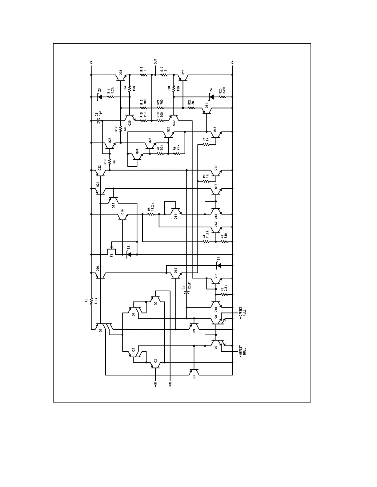
Equivalent Circuit
TL/H/10075– 3
Note: All resistor values in ohms.
5
 Loading...