

NSC LM75CIMM-3, LM75CIM-5, LM75CIM-3, LM75B-5.0MDC, LM75CIMM-5 Datasheet
LM75
Digital Temperature Sensor and Thermal WATCHDOG
™
with Two-Wire Interface
General Description
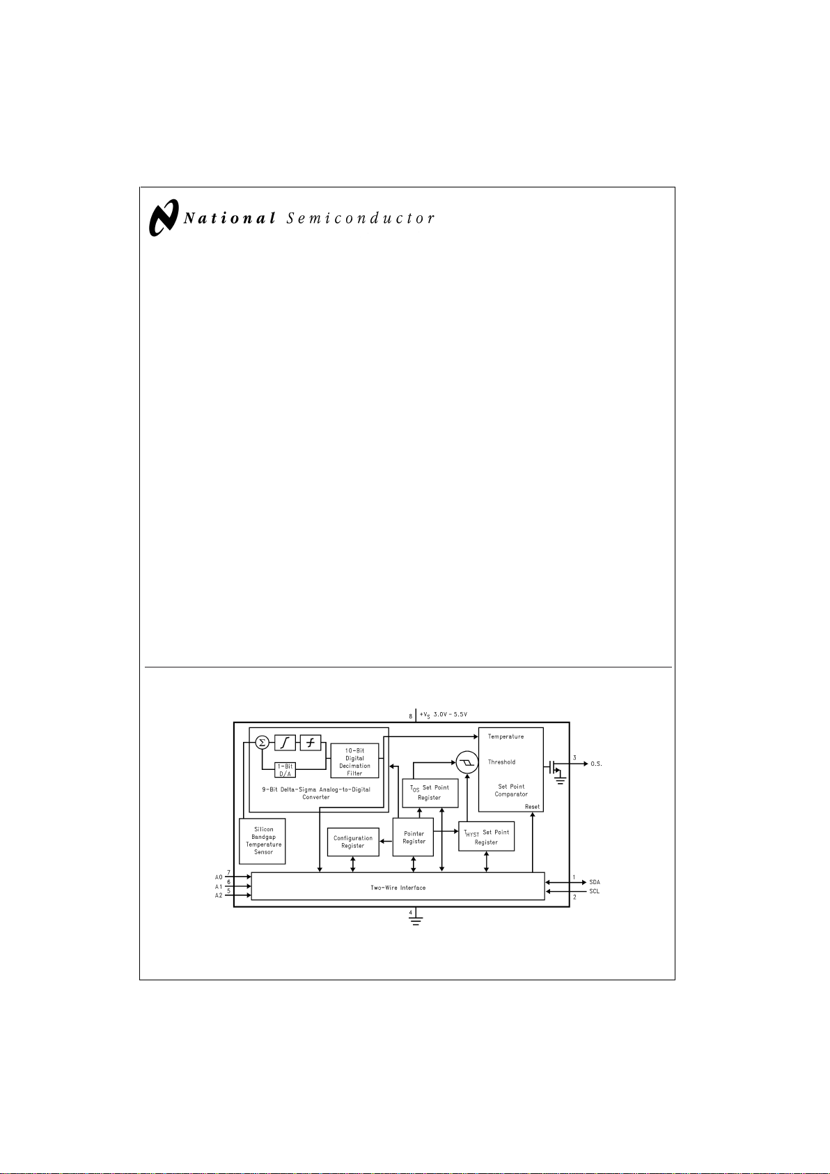
The LM75 is a temperature sensor, Delta-Sigma
analog-to-digital converter, and digital over-temperature detector with I
2
C®interface. The host can query the LM75 at
any time to read temperature. The open-drain Overtemperature Shutdown (O.S.) output becomes active when the temperature exceeds a programmable limit. This pin can operate
in either “Comparator” or “Interrupt” mode.
The host can program both the temperature alarm threshold
(T
OS
) and the temperature at which the alarm condition goes
away (T
HYST
). In addition, the host can read back the contents of the LM75’s T
OS
and T
HYST
registers. Three pins (A0,
A1,A2) are available for address selection. The sensor powers up in Comparator mode with default thresholds of 80˚C
T
OS
and 75˚C T
HYST
.
The LM75’s 3.0V to 5.5V supply voltage range, low supply
current and I
2
C interface make it ideal for a wide range of applications. These include thermal management and protection applications in personal computers, electronic test
equipment, and office electronics.
Features
n SOP-8 and Mini SOP-8 (MSOP) packages save space
n I
2
C Bus interface
n Separate open-drain output pin operates as interrupt or
comparator/thermostat output
n Register readback capability
n Power up defaults permit stand-alone operation as
thermostat
n Shutdown mode to minimize power consumption
n Up to 8 LM75s can be connected to a single bus
Key Specifications
n Supply Voltage 3.0V to 5.5V
n Supply Current operating 250 µA (typ)
1 mA (max)
shutdown 4 µA (typ)
n Temperature Accuracy −25˚C to 100˚C
±
2˚C(max)
−55˚C to 125˚C
±
3˚C(max)
Applications
n System Thermal Management
n Personal Computers
n Office Electronics
n Electronic Test Equipment
Simplified Block Diagram
WATCHDOG™is a trademark of National Semiconductor Corporation.
I2C
®
is a registered trademark of Philips Corporation.
DS012658-1
January 2000
LM75 Digital Temperature Sensor and Thermal WATCHDOG with Two-Wire Interface
© 2000 National Semiconductor Corporation DS012658 www.national.com
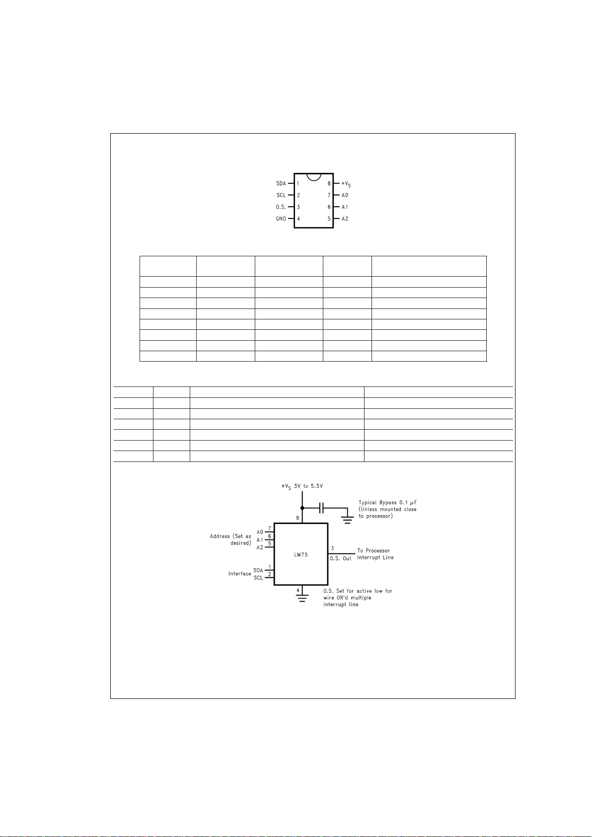
Connection Diagram
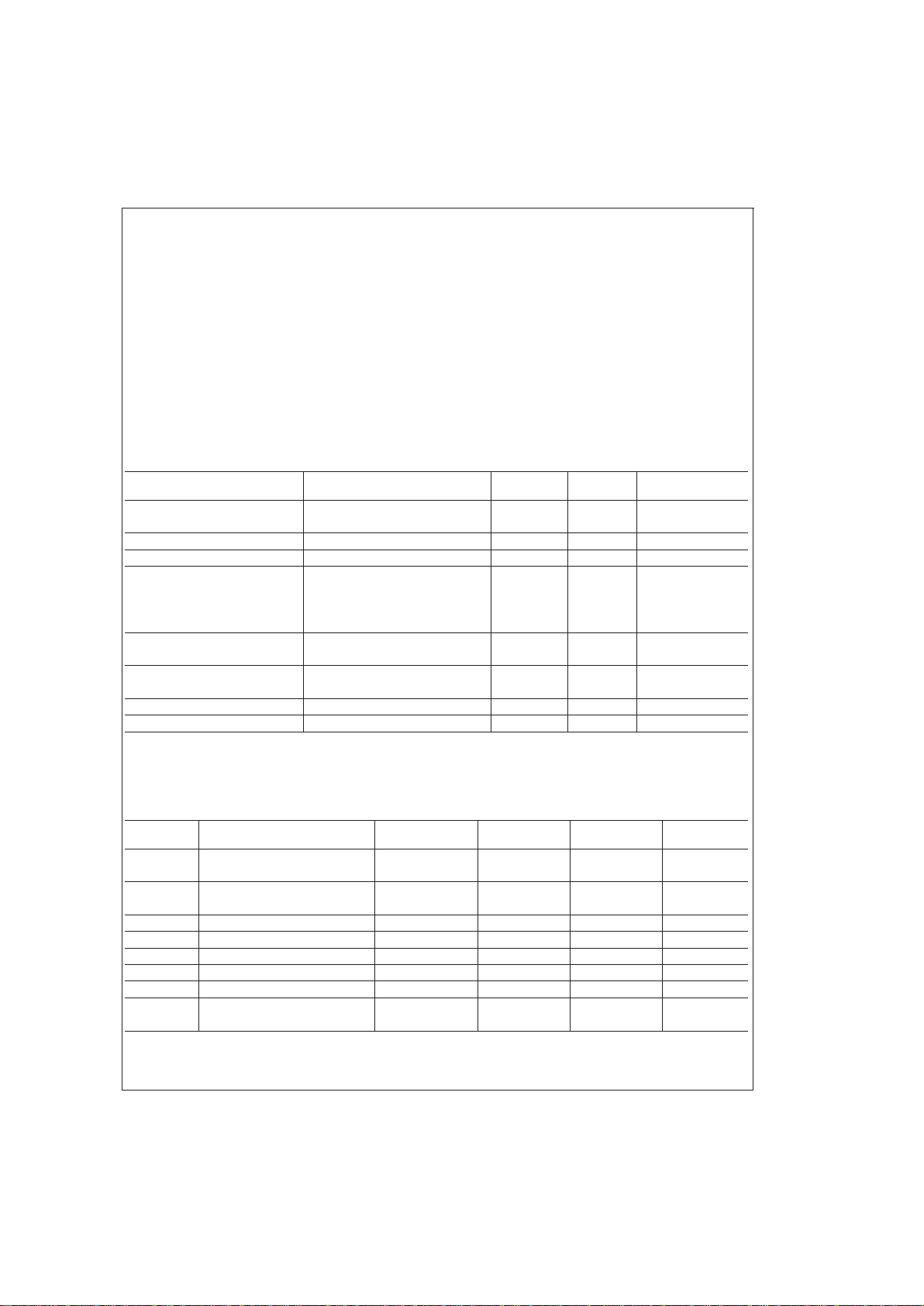
Ordering Information
Order Number
Package
Marking
NS Package
Number
Supply
Voltage
Transport Media
LM75CIM-3 LM75CIM-3 M08A (SOP-8) 3.3V
LM75CIMX-3 LM75CIM-3 M08A (SOP-8) 3.3V 2500 Units on Tape and Reel
LM75CIMM-3 T01C MUA08A (MSOP-8) 3.3V 250 Units in Rail
LM75CIMMX-3 T01C MUA08A (MSOP-8) 3.3V 3500 Units on Tape and Reel
LM75CIM-5 LM75CIM-5 M08A (SOP-8) 5V
LM75CIMX-5 LM75CIM-5 M08A (SOP-8) 5V 2500 Units on Tape and Reel
LM75CIMM-5 T00C MUA08A (MSOP-8) 5V 250 Units in Rail
LM75CIMMX-5 T00C MUA08A (MSOP-8) 5V 3500 Units on Tape and Reel
Pin Description
Label Pin
#
Function Typical Connection
SDA 1 I
2
C Serial Bi-Directional Data Line. Open Drain. From Controller, tied to a pull-up
SCL 2 I
2
C Clock Input From Controller
O.S. 3 Overtemperature Shutdown Open Drain Output Pull Up Resistor, Controller Interrupt Line
GND 4 Power Supply Ground Ground
+V
S
8 Positive Supply Voltage Input DC Voltage from 3V to 5.5V
A0–A2 7,6,5 User-Set I
2
C Address Inputs Ground (Low, “0”) or +VS(High, “1”)
SOP-8 and Mini SOP-8
DS012658-2
DS012658-3
FIGURE 1. Typical Application
LM75
www.national.com 2
Absolute Maximum Ratings (Note 1)
Supply Voltage −0.3V to 6.5V
Voltage at any Pin −0.3V to +V
S
+ 0.3V
Input Current at any Pin (Note 2) 5 mA
Package Input Current (Note 2) 20 mA
O.S. Output Sink Current 10 mA
O.S. Output Voltage 6.5V
Storage Temperature −65˚C to +150˚C
Soldering Information, Lead Temperature
SOP and MSOP Package (Note 3)
Vapor Phase (60 seconds)
Infrared (15 seconds)
215˚C
220˚C
ESD Susceptibility (Note 4)
Human Body Model 950V
Machine Model 100V
Operating Ratings
Specified Temperature Range T
MIN
to T
MAX
(Note 5) −55˚C to +125˚C
Supply Voltage Range (+V
S
) +3.0V to +5.5V
Temperature-to-Digital Converter Characteristics
Unless otherwise noted, these specifications apply for +V
S
=
+5 Vdc for LM75CIM-5 and LM75CIMM-5 and +V
S
=
+3.3 Vdc for
LM75CIM-3 and LM75CIMM-3 (Note 6). Boldface limits apply for T
A
=
T
J
=
T
MIN
to T
MAX
; all other limits T
A
=
T
J
=
+25˚C,
unless otherwise noted.
Parameter Conditions
Typical
(Note 12)
Limits
(Note 7)
Units
(Limit)
Accuracy T
A
=
−25˚C to +100˚C
±
2.0 ˚C (max)
T
A
=
−55˚C to +125˚C
±
3.0
Resolution 9 Bits
Temperature Conversion Time (Note 8) 100 ms
Quiescent Current I
2
C Inactive 0.25 mA
I
2
C Active 1.0 mA (max)
Shutdown Mode, +V
S
=
3V 4 µA
Shutdown Mode, +V
S
=
5V 6 µA
O.S. Output Saturation Voltage I
OUT
=
4.0 mA 0.8 V (max)
(Note 9)
O.S. Delay (Note 10) 1 Conversions (min)
6 Conversions (max)
T
OS
Default Temperature (Note 11) 80 ˚C
T
HYST
Default Temperature (Note 11) 75 ˚C
Logic Electrical Characteristics
DIGITAL DC CHARACTERISTICS
Unless otherwise noted, these specifications apply for +V
S
=
+5 Vdc for LM75CIM-5 and LM75CIMM-5 and +V
S
=
+3.3 Vdc for
LM75CIM-3 and LM75CIMM-3. Boldface limits apply for T
A
=
T
J
=
T
MIN
to T
MAX
; all other limits T
A
=
T
J
=
+25˚C, unless
otherwise noted.
Symbol Parameter Conditions
Typical
(Note 12)
Limits
(Note 7)
Units
(Limit)
V
IN(1)
Logical “1” Input Voltage +VSx 0.7 V (min)
+V
S
+0.5 V (max)
V
IN(0)
Logical “0” Input Voltage −0.3 V (min)
+V
S
x 0.3 V (max)
I
IN(1)
Logical “1” Input Current V
IN
=
5V 0.005 1.0 µA (max)
I
IN(0)
Logical “0” Input Current V
IN
=
0V −0.005 −1.0 µA (max)
C
IN
All Digital Inputs 20 pF
I
OH
High Level Output Current V
OH
=
5V 100 µA (max)
V
OL
Low Level Output Voltage I
OL
=
3mA 0.4 V (max)
t
OF
Output Fall Time C
L
=
400 pF 250 ns (max)
I
O
=
3mA
LM75
www.national.com3
Logic Electrical Characteristics (Continued)
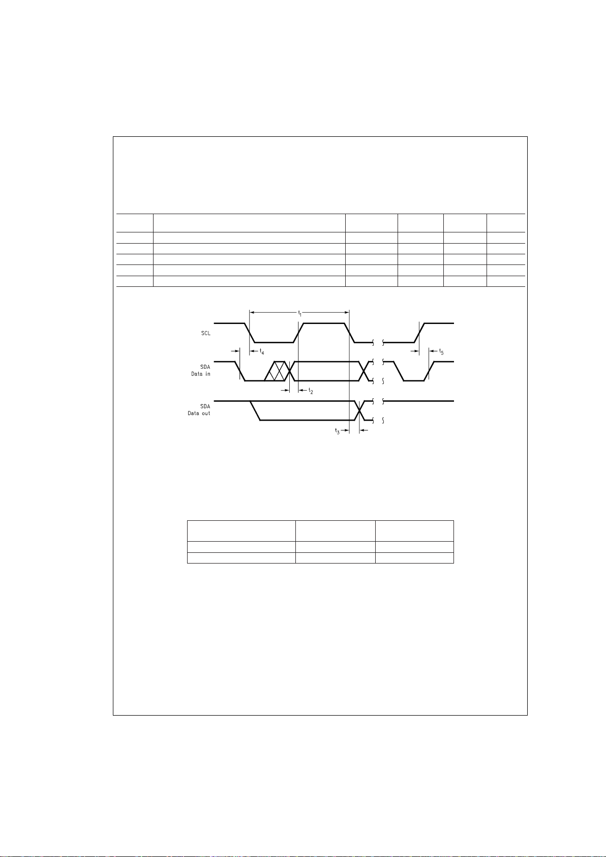
I2C DIGITAL SWITCHING CHARACTERISTICS
Unless otherwise noted, these specifications apply for+V
S
=
+5 Vdc for LM75CIM-5 and LM75CIMM-5 and +V
S
=
+3.3 Vdc for
LM75CIM-3 and LM75CIMM-3 , C
L
(load capacitance) on output lines=80 pF unless otherwise specified. Boldface limits
apply for T
A
=
T
J
=
T
MIN
to T
MAX
; all other limits T
A
=
T
J
=
+25˚C, unless otherwise noted.
The switching characteristics of the LM75 fully meet or exceed the published specifications of the I
2
C bus. The following pa-
rameters are the timing relationships between SCL and SDA signals related to the LM75. They are not the I
2
C bus specifica-
tions.
Symbol Parameter Conditions
Typical
(Note 12)
Limits
(Note 7)
Units
(Limit)
t
1
SCL (Clock) Period 2.5 µs(min)
t
2
Data in Set-Up Time to SCL High 100 ns(min)
t
3
Data Out Stable after SCL Low 0 ns(min)
t
4
SDA Low Set-Up Time to SCL Low (Start Condition) 100 ns(min)
t
5
SDA High Hold Time after SCL High (Stop Condition) 100 ns(min)
Note 1: AbsoluteMaximumRatingsindicate limits beyond which damage to the device may occur. DC and AC electrical specifications do not apply when operating
the device beyond its rated operating conditions.
Note 2: When the input voltage (V
I
) at any pin exceeds the power supplies (V
I
<
GND or V
I
>
+VS) the current at that pin should be limited to 5 mA. The 20 mA
maximum package input current rating limits the number of pins that can safely exceedthe power supplies with an input current of 5 mA to four.
Note 3: SeeAN-450 “Surface Mounting Methods and Their Effect on Product Reliability” or the section titled “Surface Mount” found in a current National Semicon-
ductor Linear Data Book for other methods of soldering surface mount devices.
Note 4: Human body model, 100 pF discharged through a 1.5 kΩ resistor. Machine model, 200 pF discharged directly into each pin.
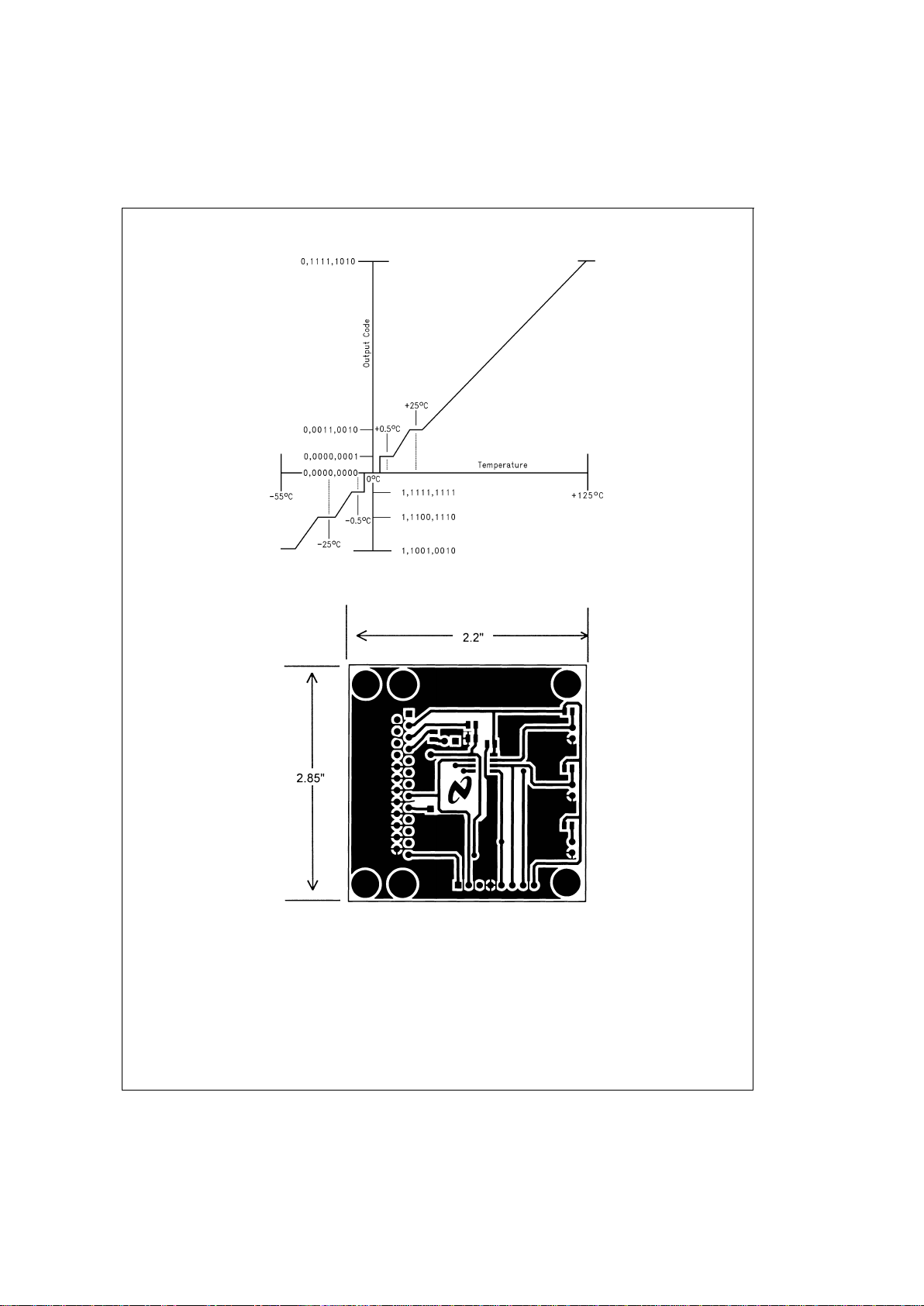
Note 5: LM75θ
JA
(thermal resistance, junction-to-ambient) when attached to a printed circuit board with 2 oz. foil similar to the one shown in
Figure 3
is summarized
in the table below:
Device Number
NS Package
Number
Thermal
Resistance (θ
JA
)
LM75CIM-3, LM75CIM-5 M08A 200˚C/W
LM75CIMM-3, LM75CIMM-5 MUA08A 250˚C/W
Note 6: Both part numbers of the LM75 will operate properly over the +VSsupply voltage range of 3V to 5.5V.The devices are tested and specified for rated ac-
curacy at their nominal supply voltage. Accuracy will typically degrade 1˚C/V of variation in +V
S
as it varies from the nominal value.
Note 7: Limits are guaranteed to National’s AOQL (Average Outgoing Quality Level).
Note 8: Thisspecification is provided only to indicate how often temperature data is updated. The LM75 can be read at any time without regard to conversion state
(and will yield last conversion result). If a conversion is in process it will be interrupted and restarted after the end of the read.
Note 9: Forbest accuracy, minimize output loading. Higher sink currents can affect sensor accuracy with internal heating. This can cause an error of 0.64˚C at full
rated sink current and saturation voltage based on junction-to-ambient thermal resistance.
Note 10: O.S. Delay is user programmable up to 6 “over limit” conversions before O.S. is set to minimize false tripping in noisy environments.
Note 11: Default values set at power up.
Note 12: Typicals are at T
A
=
25˚C and represent most likely parametric norm.
DS012658-4
LM75
www.national.com 4
Logic Electrical Characteristics (Continued)
DS012658-5
FIGURE 2. Temperature-to-Digital Transfer Function (Non-linear scale for clarity)
DS012658-6
FIGURE 3. Printed Circuit Board Used for Thermal Resistance Specifications
LM75
www.national.com5
 Loading...