NSC LM733CN, LM733H, LM733CH Datasheet

LM733/LM733C Differential Amplifier
LM733/LM733C Differential Amplifier
August 1989
General Description
The LM733/LM733C is a two-stage, differential input, differential output, wide-band video amplifier. The use of internal
series-shunt feedback gives wide bandwidth with low phase
distortion and high gain stability. Emitter-follower outputs
provide a high current drive, low impedance capability. Its
120 MHz bandwidth and selectable gains of 10, 100 and
400, without need for frequency compensation, make it a
very useful circuit for memory element drivers, pulse amplifiers, and wide band linear gain stages.
The LM733 is specified for operation over the
a
125§C military temperature range. The LM733C is speci-
fied for operation over the 0
Ctoa70§C temperature range.
§
b
55§Cto
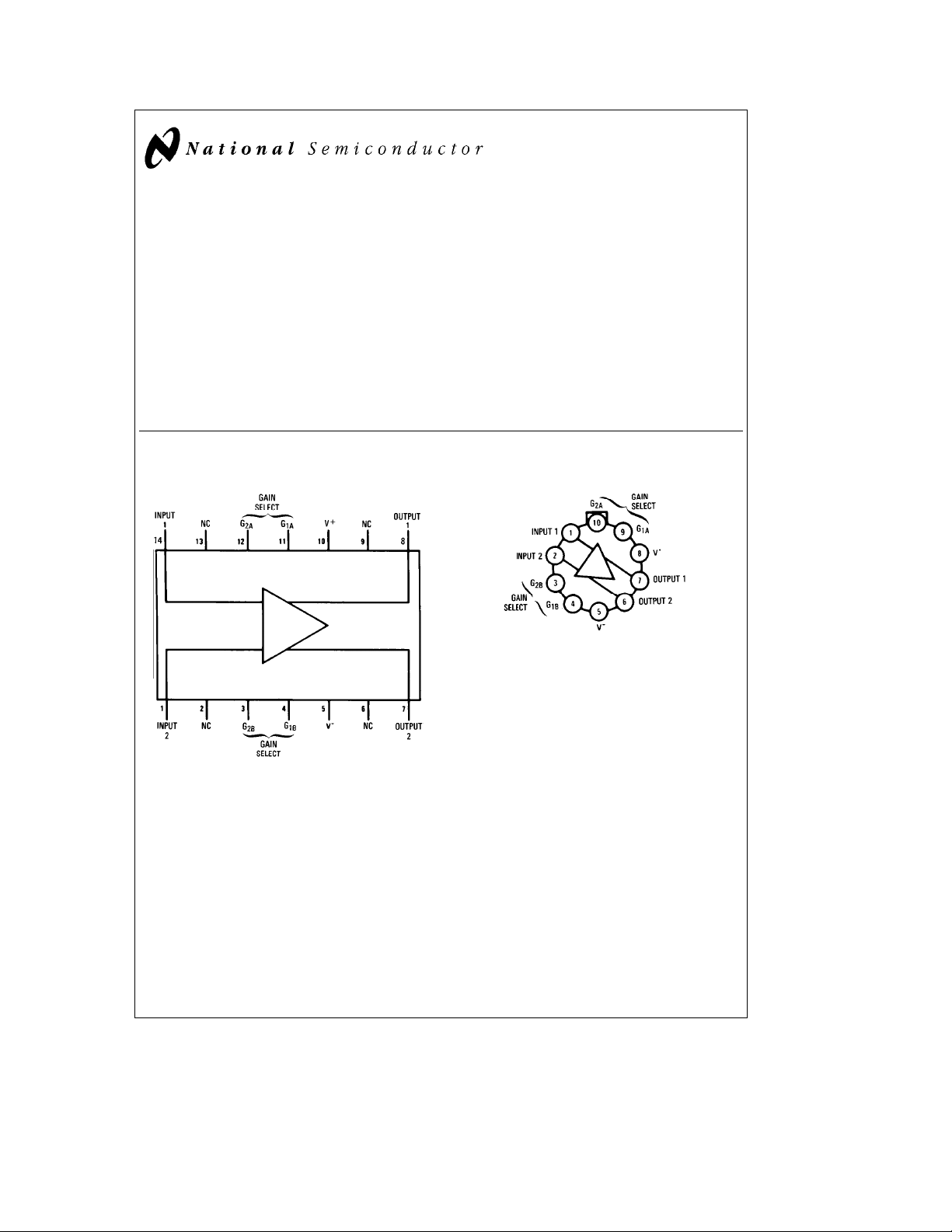
Connection Diagrams
Dual-In-Line Package
Features
Y
120 MHz bandwidth
Y
250 kX input resistance
Y
Selectable gains of 10, 100, 400
Y
No frequency compensation
Y
High common mode rejection ratio at high frequencies
Applications
Y
Magnetic tape systems
Y
Disk file memories
Y
Thin and thick film memories
Y
Woven and plated wire memories
Y
Wide band video amplifiers
Metal Can Package
Note: Pin 5 connected to case.
Top View
Order Number LM733H or LM733CH
See NS Package Number H10D
TL/H/7866– 2
Top View
TL/H/7866– 1
Order Number LM733CN
See NS Package Number N14A
C
1995 National Semiconductor Corporation RRD-B30M115/Printed in U. S. A.
TL/H/7866

Absolute Maximum Ratings
If Military/Aerospace specified devices are required,
please contact the National Semiconductor Sales
Office/Distributors for availability and specifications.
Diffential Input Voltage
Common Mode Input Voltage
V
CC
Output Current 10 mA
g
5V
g
6V
g
8V
Power Dissipation (Note 1) 500 mW
Junction Temperature
Storage Temperature Range
Operating Temperature Range
LM733
LM733C 0
b
b
a
150§C
65§Ctoa150§C
55§Ctoa125§C
Ctoa70§C
§
Lead Temperature (Soldering, 10 sec.) 260§C
Electrical Characteristics (T
Characteristics
Test
Circuit
e
25§C, unless otherwise specified, see test circuits, V
A
Test Conditions
LM733 LM733C
Min Typ Max Min Typ Max
e
g
6.0V)
S
Units
Differential Voltage Gain
Gain 1 (Note 2) 300 400 500 250 400 600
Gain 2 (Note 3) 1 90 100 110 80 100 120
Gain 3 (Note 4) R
L
e
2kXV
e
3 Vp-p 9.0 10 11 8.0 10 12
OUT
Bandwidth
Gain 1 40 40 MHz
Gain 2 2 90 90 MHz
Gain 3 120 120 MHz
Rise Time
Gain 1 V
Gain 2 2 4.5 10 4.5 12 ns
e
1 Vp-p 10.5 10.5 ns
OUT
Gain 3 2.5 2.5 ns
Propagation Delay V
Gain 1 7.5 7.5 ns
OUT
e
1 Vp-p
Gain 2 2 6.0 10 6.0 10 ns
Gain 3 3.6 3.6 ns
Input Resistance
Gain 1 4.0 4.0 kX
Gain 2 20 30 10 30 kX
Gain 3 250 250 kX
Input Capacitance Gain 2 2.0 2.0 pF
Input Offset Current 0.4 3.0 0.4 5.0 mA
Input Bias Current 9.0 20 9.0 30 mA
Input Noise Voltage BWe1 kHz to 10 MHz 12 12 mVrms
Input Voltage Range 1
g
1.0
g
1.0 V
Common Mode Rejection Ratio
e
Gain 2 1 V
Gain 2 V
g
1V fs100 kHz 60 86 60 86 dB
CM
e
g
1V fe5 MHz 60 60 dB
CM
Supply Voltage Rejection Ratio
e
Gain 2 1 DV
g
0.5V 50 70 50 70 dB
S
Output Offset Voltage
Gain 1 1 R
Gain 2 and 3 0.35 1.0 0.35 1.5 V
Output Common Mode Voltage 1 R
Output Voltage Swing 1 R
e %
L
e %
L
e
2k 3.0 4.0 3.0 4.0
L
0.6 1.5 0.6 1.5 V
2.4 2.9 3.4 2.4 2.9 3.4 V
Output Sink Current 2.5 3.6 2.5 3.6 mA
Output Resistance 20 20 X
Power Supply Current 1 R
L
e %
18 24 18 24 mA
2
 Loading...