

LM7121
235 MHz Tiny Low Power Voltage Feedback Amplifier
General Description
The LM7121 is a high performance operational amplifier
which addresses the increasing AC performance needs of
video and imaging applications, and the size and power constraints of portable applications.
The LM7121 can operate over a wide dynamic range of supply voltages, from5V(singlesupply) up to
±
15V (see the Application Information section for more details). It offers an excellent speed-power product delivering 1300V/µs and 235
MHz Bandwidth (−3 dB,A
V
=
+1).Another key feature of this
operational amplifier is stability while driving unlimited capacitive loads.
Due to its Tiny SOT23-5 package, the LM7121 is ideal for
designs where space and weight are the critical parameters.
The benefits of the Tiny package are evident in small portable electronic devices, such as cameras, and PC video
cards. Tiny amplifiers are so small that they can be placed
anywhere on a board close to the signal source or near the
input to an A/D converter.
Features
(Typical unless otherwise noted) V
S
=
±
15V
n Easy to use voltage feedback topology
n Stable with unlimited capacitive loads
n Tiny SOT23-5 package—typical circuit layout takes half
the space of SO-8 designs
n Unity gain frequency: 175 MHz
n Bandwidth (−3 dB, A
V
=
+1, R
L
=
100Ω): 235 MHz
n Slew rate: 1300V/µs
n Supply Voltages SO-8: 5V to
±
15V
SOT23-5: 5V to
±
5V
n Characterized for: +5V,
±
5V,±15V
n Low supply current: 5.3 mA
Applications
n Scanners, color fax, digital copiers
n PC video cards
n Cable drivers
n Digital cameras
n ADC/DAC buffers
n Set-top boxes
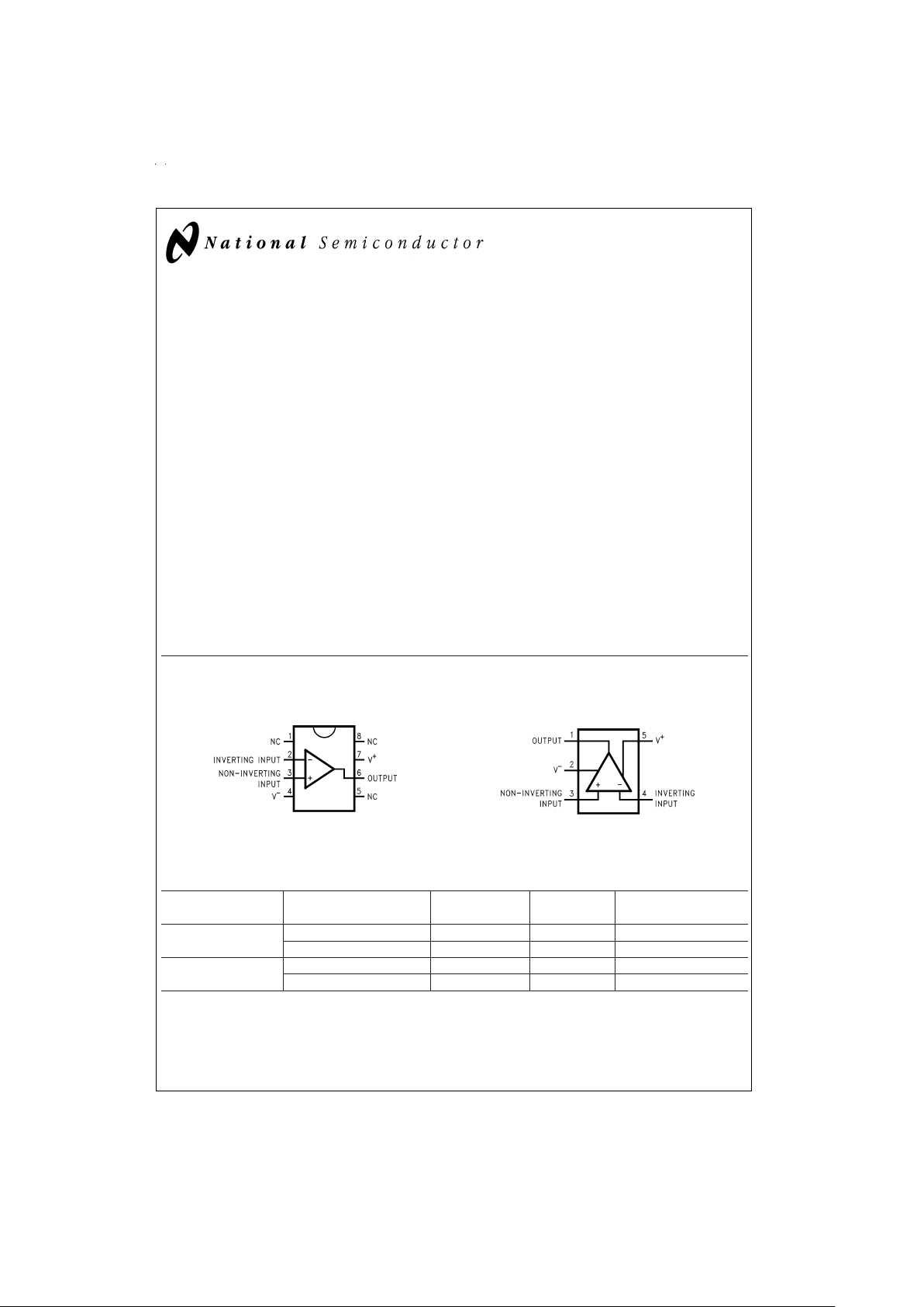
Connection Diagrams
Ordering Information
Package Ordering Information NSC Drawing Package Supplied As
Number Marking
8-Pin SO-8 LM7121IM M08A LM7121IM Rails
LM7121IMX M08A LM7121IM 2.5k Tape and Reel
5-Pin SOT23-5 LM7121IM5 MA05A A03A 1k Tape and Reel
LM7121IM5X MA05A A03A 3k Tape and Reel
8-Pin SO-8
DS012348-2
Top View
5-Pin SOT23
DS012348-1
Top View
August 1999
LM7121 235 MHz Tiny Low Power Voltage Feedback Amplifier
© 1999 National Semiconductor Corporation DS012348 www.national.com
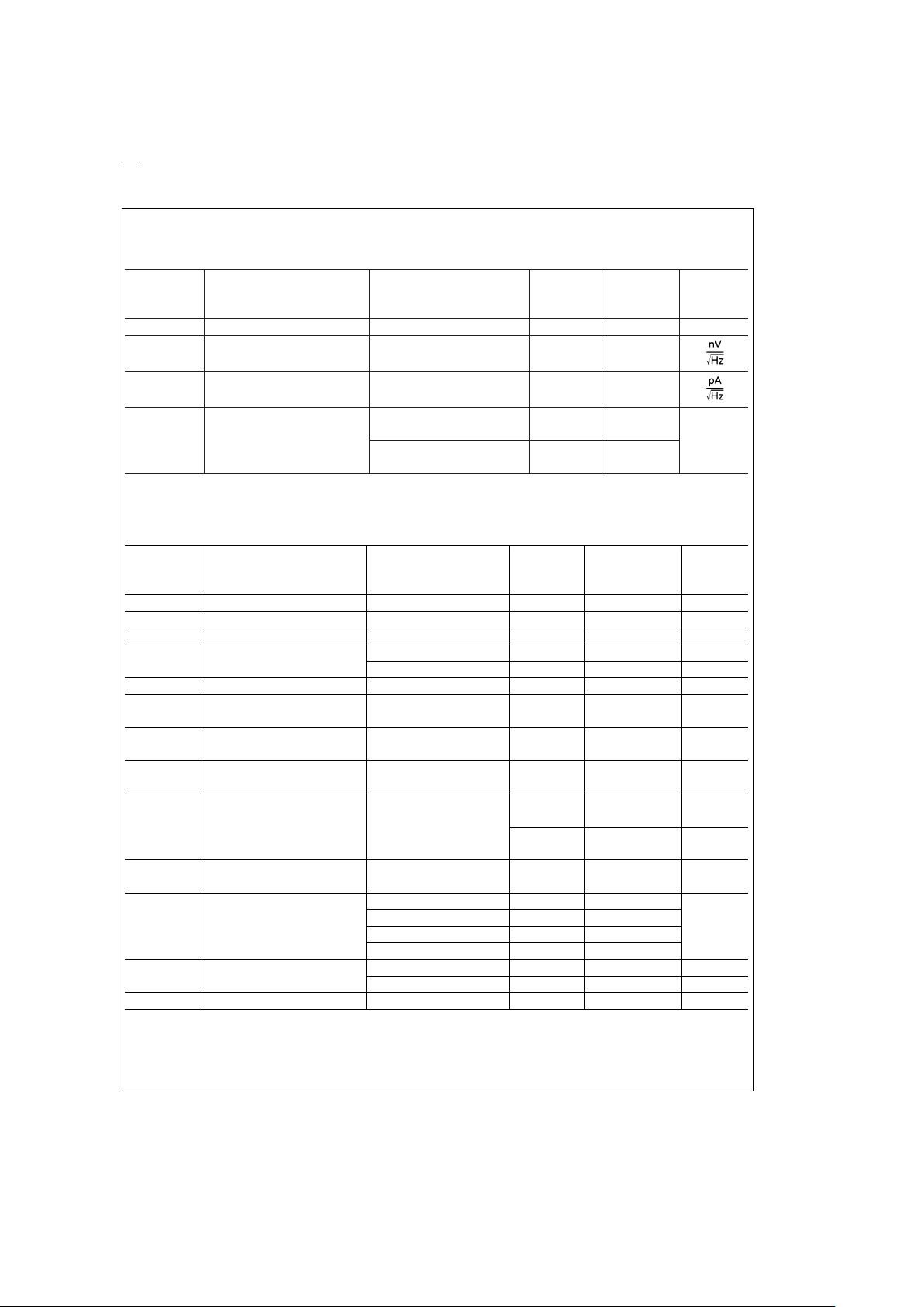
Absolute Maximum Ratings (Note 1)
If Military/Aerospace specified devices are required,
please contact the National Semiconductor Sales Office/
Distributors for availability and specifications.
ESD Tolerance (Note 2) 2000V
Differential Input Voltage (Note 7)
±
2V
Voltage at Input/Output Pin (V
+
)−1.4V, (V−)+1.4V
Supply Voltage (V
+–V−
) 36V
Output Short Circuit to Ground
(Note 3) Continuous
Lead Temperature 260˚C
(soldering, 10 sec) 260˚C
Storage Temperature Range −65˚C to +150˚C
Junction Temperature (Note 4) 150˚C
Operating Ratings (Note 1)
Supply Voltage: SO-8 4.5V ≤ V
S
≤ 33V
SOT23-5 4.5V ≤ V
S
≤ 11V
Junction Temperature Range −40˚C ≤ T
J
≤ +85˚C
Thermal Resistance (θ
JA
)
M Package, 8-pin Surface Mount 165˚C/W
SOT23-5 Package 325˚C/W
±
15V DC Electrical Characteristics
Unless otherwise specified, all limits guaranteed for T
J
=
25˚C, V
+
=
+15V, V
−
=
−15V, V
CM
=
V
O
=
0V and R
L
>
1MΩ.
Boldface limits apply at the temperature extremes.
Symbol Parameter Conditions Typ
(Note 5)
LM7121I Units
Limit
(Note 6)
V
OS
Input Offset Voltage 0.9 8 mV
15 max
I
B
Input Bias Current 5.2 9.5 µA
12 max
I
OS
Input Offset Current 0.04 4.3 µA
7 max
R
IN
Input Resistance Common Mode 10 MΩ
Differential Mode 3.4 MΩ
C
IN
Input Capacitance Common Mode 2.3 pF
CMRR Common Mode −10V ≤ V
CM
≤ 10V 93 73 dB
Rejection Ratio 70 min
+PSRR Positive Power Supply 10V ≤ V
+
≤ 15V 86 70 dB
Rejection Ratio 68 min
−PSRR Negative Power Supply −15V ≤ V
−
≤ −10V 81 68 dB
Rejection Ratio 65 min
V
CM
Input Common-Mode CMRR ≥ 70 dB 13 11 V
Voltage Range min
−13 −11 V
max
A
V
Large Signal R
L
=
2kΩ,V
O
=
20 V
PP
72 65 dB
Voltage Gain 57 min
V
O
Output Swing R
L
=
2kΩ 13.4 11.1 V
10.8 min
−13.4 −11.2 V
−11.0 max
R
L
=
150Ω 10.2 7.75 V
7.0 min
−7.0 −5.0 V
−4.8 max
I
SC
Output Short Circuit Sourcing 71 54 mA
Current 44 min
Sinking 52 39 mA
34 min
www.national.com 2
±
15V DC Electrical Characteristics (Continued)
Unless otherwise specified, all limits guaranteed for T
J
=
25˚C, V
+
=
+15V, V
−
=
−15V, V
CM
=
V
O
=
0V and R
L
>
1MΩ.
Boldface limits apply at the temperature extremes.
Symbol Parameter Conditions Typ
(Note 5)
LM7121I Units
Limit
(Note 6)
I
S
Supply Current 5.3 6.6 mA
7.5 max
±
15V AC Electrical Characteristics
Unless otherwise specified, all limits guaranteed for T
J
=
25˚C, V
+
=
15V, V
−
=
−15V, V
CM
=
V
O
=
0V and R
L
>
1MΩ.Bold-
face limits apply at the temperature extremes.
Symbol Parameter Conditions Typ
(Note 5)
LM7121I Units
Limit
(Note 6)
SR Slew Rate A
V
=
+2, R
L
=
1kΩ, 1300 V/µs
(Note 8) V
O
=
20 V
PP
GBW Unity Gain-Bandwidth R
L
=
1kΩ 175 MHz
φ
m
Phase Margin 63 Deg
f (−3 dB) Bandwidth R
L
=
100Ω,A
V
=
+1 235 MHz
(Notes 9, 10) R
L
=
100Ω,A
V
=
+2 50
t
s
Settling Time 10 VPPStep, to 0.1%,74 ns
R
L
=
500Ω
t
r,tf
Rise and Fall Time A
V
=
+2, R
L
=
100Ω, 5.3 ns
(Note 10) V
O
=
0.4 V
PP
A
D
Differential Gain A
V
=
+2, R
L
=
150Ω 0.3
%
φ
D
Differential Phase A
V
=
+2, R
L
=
150Ω 0.65 Deg
e
n
Input-Referred f=10 kHz
17
Voltage Noise
i
n
Input-Referred f=10 kHz
1.9
Current Noise
T.H.D. Total Harmonic Distortion 2 V
PP
Output, R
L
=
150Ω, 0.065
%
A
V
=
+2, f=1 MHz
2V
PP
Output, R
L
=
150Ω, 0.52
A
V
=
+2, f=5 MHz
±
5V DC Electrical Characteristics
Unless otherwise specified, all limits guaranteed for T
J
=
25˚C, V
+
=
5V, V
−
=
−5V, V
CM
=
V
O
=
0V and R
L
>
1MΩ.Bold-
face limits apply at the temperature extremes.
Symbol Parameter Conditions Typ
(Note 5)
LM7121I Units
Limit
(Note 6)
V
OS
Input Offset Voltage 1.6 8 mV
15 max
I
B
Input Bias Current 5.5 9.5 µA
12 max
I
OS
Input Offset Current 0.07 4.3 µA
7.0 max
R
IN
Input Resistance Common Mode 6.8 MΩ
Differential Mode 3.4 MΩ
www.national.com3
±
5V DC Electrical Characteristics (Continued)
Unless otherwise specified, all limits guaranteed for T
J
=
25˚C, V
+
=
5V, V
−
=
−5V, V
CM
=
V
O
=
0V and R
L
>
1MΩ.Bold-
face limits apply at the temperature extremes.
Symbol Parameter Conditions Typ
(Note 5)
LM7121I Units
Limit
(Note 6)
C
IN
Input Capacitance Common Mode 2.3 pF
CMRR Common Mode −2V ≤ V
CM
≤ 2V 75 65 dB
Rejection Ratio 60 min
+PSRR Positive Power Supply 3V ≤ V
+
≤ 5V 89 65 dB
Rejection Ratio 60 min
−PSRR Negative Power Supply −5V ≤ V
−
≤ −3V 78 65 dB
Rejection Ratio 60 min
V
CM
Input Common Mode CMRR ≥ 60 dB 3 2.5 V
Voltage Range min
−3 −2.5 V
max
A
V
Large Signal R
L
=
2kΩ,V
O
=
3V
PP
66 60 dB
Voltage Gain 58 min
V
O
Output Swing R
L
=
2kΩ 3.62 3.0 V
2.75 min
−3.62 −3.0 V
−2.70 max
R
L
=
150Ω 3.1 2.5 V
2.3 min
−2.8 −2.15 V
−2.00 max
I
SC
Output Short Circuit Sourcing 53 38 mA
Current 33 min
Sinking 29 21 mA
19 min
I
S
Supply Current 5.1 6.4 mA
7.2 max
±
5V AC Electrical Characteristics
Unless otherwise specified, all limits guaranteed for T
J
=
25˚C, V
+
=
5V, V
−
=
−5V, V
CM
=
V
O
=
0V and R
L
>
1MΩ.Bold-
face limits apply at the temperature extremes.
Symbol Parameter Conditions Typ
(Note 5)
LM7121I Units
Limit
(Note 6)
SR Slew Rate A
V
=
+2, R
L
=
1kΩ, 520 V/µs
(Note 8) V
O
=
6V
PP
GBW Unity Gain-Bandwidth R
L
=
1kΩ 105 MHz
φ
m
Phase Margin R
L
=
1kΩ 74 Deg
f (−3 dB) Bandwidth R
L
=
100Ω,A
V
=
+1 160 MHz
(Notes 9, 10) R
L
=
100Ω,A
V
=
+2 50
t
s
Settling Time 5 VPPStep, to 0.1%,65 ns
R
L
=
500Ω
t
r,tf
Rise and Fall Time A
V
=
+2, R
L
=
100Ω, 5.8 ns
(Note 10) V
O
=
0.4 V
PP
A
D
Differential Gain A
V
=
+2, R
L
=
150Ω 0.3
%
www.national.com 4
±
5V AC Electrical Characteristics (Continued)
Unless otherwise specified, all limits guaranteed for T
J
=
25˚C, V
+
=
5V, V
−
=
−5V, V
CM
=
V
O
=
0V and R
L
>
1MΩ.Bold-
face limits apply at the temperature extremes.
Symbol Parameter Conditions Typ
(Note 5)
LM7121I Units
Limit
(Note 6)
φ
D
Differential Phase A
V
=
+2, R
L
=
150Ω 0.65 Deg
e
n
Input-Referred f=10 kHz
17
Voltage Noise
i
n
Input-Referred f=10 kHz
2
Current Noise
T.H.D. Total Harmonic Distortion 2 V
PP
Output, R
L
=
150Ω, 0.1
%
A
V
=
+2, f=1 MHz
2V
PP
Output, R
L
=
150Ω, 0.6
A
V
=
+2, f=5 MHz
+5V DC Electrical Characteristics
Unless otherwise specified, all limits guaranteed for T
J
=
25˚C, V
+
=
+5V, V
−
=
0V, V
CM
=
V
O
=
V
+
/2 and R
L
>
1MΩ.Bold-
face limits apply at the temperature extremes.
Symbol Parameter Conditions Typ
(Note 5)
LM7121I Units
Limit
(Note 6)
V
OS
Input Offset Voltage 2.4 mV
I
B
Input Bias Current 4 µA
I
OS
Input Offset Current 0.04 µA
R
IN
Input Resistance Common Mode 2.6 MΩ
Differential Mode 3.4 MΩ
C
IN
Input Capacitance Common Mode 2.3 pF
CMRR Common Mode 2V ≤ V
CM
≤ 3V 65 dB
Rejection Ratio
+PSRR Positive Power Supply 4.6V ≤ V
+
≤ 5V 85 dB
Rejection Ratio
−PSRR Negative Power Supply 0V ≤ V
−
≤ 0.4V 61 dB
Rejection Ratio
V
CM
Input Common-Mode CMRR ≥ 45 dB 3.5 V
Voltage Range min
1.5 V
max
A
V
Large Signal R
L
=
2kΩto V
+
/2 64 dB
Voltage Gain
V
O
Output Swing R
L
=
2kΩto V
+
/2, High 3.7 V
R
L
=
2kΩto V
+
/2, Low 1.3
R
L
=
150Ω to V
+
/2, High 3.48
R
L
=
150Ω to V
+
/2, Low 1.59
I
SC
Output Short Circuit Sourcing 33 mA
Current Sinking 20 mA
I
S
Supply Current 4.8 mA
www.national.com5
+5V AC Electrical Characteristics
Unless otherwise specified, all limits guaranteed for T
J
=
25˚C, V
+
=
+5V, V
−
=
0V, V
CM
=
V
O
=
V
+
/2 and R
L
>
1MΩ.Bold-
face limits apply at the temperature extremes.
Symbol Parameter Conditions Typ
(Note 5)
LM7121I Units
Limit
(Note 6)
SR Slew Rate A
V
=
+2, R
L
=
1kΩto 145 V/µs
(Note 8) V
+
/2, V
O
=
1.8 V
PP
GBW Unity Gain-Bandwidth R
L
=
1k, to V
+
/2 80 MHz
φ
m
Phase Margin R
L
=
1k to V
+
/2 70 Deg
f (−3 dB) Bandwidth R
L
=
100Ω to V
+
/2, A
V
=
+1 200 MHz
(Notes 9, 10) R
L
=
100Ω to V
+
/2, A
V
=
+2 45
t
r,tf
Rise and Fall Time A
V
=
+2, R
L
=
100Ω,8 ns
(Note 10) V
O
=
0.2 V
PP
T.H.D. Total Harmonic Distortion 0.6 VPPOutput, R
L
=
150Ω, 0.067
%
A
V
=
+2, f=1 MHz
0.6 V
PP
Output, R
L
=
150Ω, 0.33
A
V
=
+2, f=5 MHz
Note 1: Absolute Maximum Ratings indicate limits beyond which damage to the device may occur. Operating Ratings indicate conditions for which the device is intended to be functional, but specific performance is not guaranteed. For guaranteed specifications and the test conditions, see the Electrical Characteristics.
Note 2: Human body model, 1.5 kΩ in series with 100 pF.
Note 3: Applies to both single-supply and split-supply operation. Continuous short circuit operation at elevated ambient temperature can result in exceeding the
maximum allowed junction temperature of 150˚C.
Note 4: The maximum power dissipation is a function of T
J(max)
, θJA, and TA. The maximum allowable power dissipation at any ambient temperature is P
D
=
(T
J(max)–TA
)/θJA. All numbers apply for packages soldered directly into a PC board.
Note 5: Typical Values represent the most likely parametric norm.
Note 6: All limits are guaranteed by testing or statistical analysis.
Note 7: Differential input voltage is measured at V
S
=
±
15V.
Note 8: Slew rate is the average of the rising and fallng slew rates.
Note 9: Unity gain operation for
±
5V and±15V supplies is with a feedback network of 510Ω and 3 pF in parallel (see the Application Information section). For +5V
single supply operation, feedback is a direct short from the output to the inverting input.
Note 10: A
V
=
+2 operation with 2 kΩ resistors and 2 pF capacitor from summing node to ground.
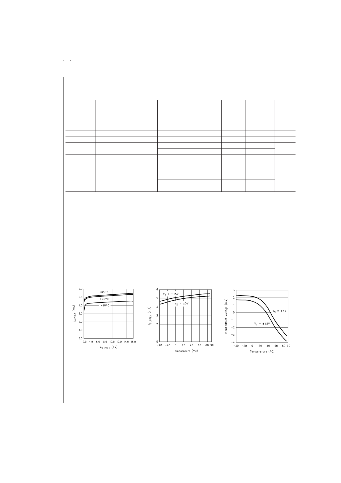
Typical Performance Characteristics T
A
=
25˚C, R
L
=
1MΩ. unless otherwise specified
Supply Current vs
Supply Voltage
DS012348-66
Supply Current vs
Temperature
DS012348-67
Input Offset Voltage
vs Temperature
DS012348-68
www.national.com 6
 Loading...