

NSC LM710H, LM710CN, LM710CH, LM710AMJ-883, LM710AMH-883 Datasheet
...
LM710
Voltage Comparator
General Description
The LM710 series are high-speed voltage comparators intended for use as an accurate, low-level digital level sensor
or as a replacement for operational amplifiers in comparator
applications where speed is of prime importance.The circuit
has a differential input and a single-ended output, with saturated output levels compatible with practically all types of integrated logic.
The device is built on a single silicon chip which insures low
offset and thermal drift. The use of a minimum number of
stages along with minority-carrier lifetime control (gold doping) makes the circuit much faster than operational amplifi-
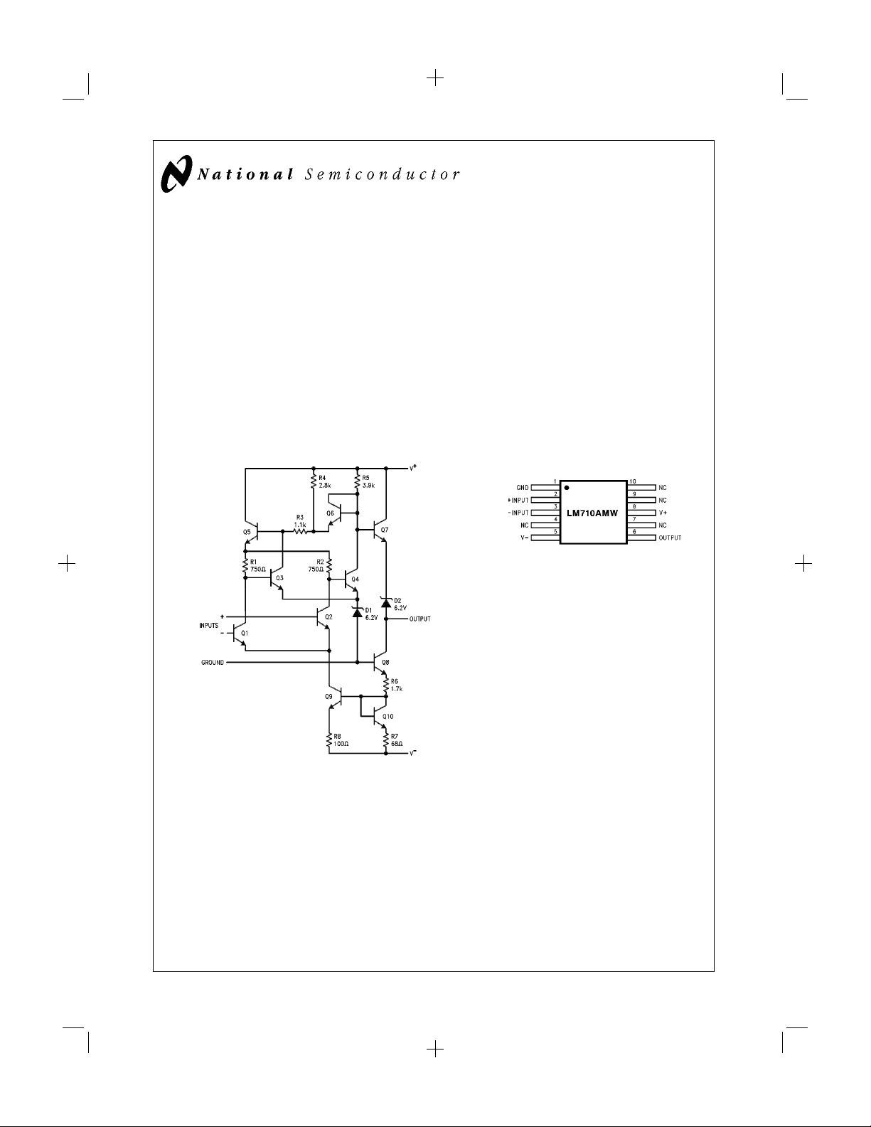
Schematic and Connection Diagrams
February 1995
ers in saturating comparator applications. In fact, the low
stray and wiring capacitances that can be realized with
monolithic construction make the device difficult to duplicate
with discrete components operating at equivalent power levels.
The LM710 series are useful as pulse height discriminators,
voltage comparators in high-speed A/D converters or go,
no-go detectors in automatic test equipment. They also have
applications in digital systems as an adjustable-threshold
line receiver or an interface between logic types. In addition,
the low cost of the units suggests them for applications replacing relatively simple discrete component circuitry.
Ceramic Flatpak Package
LM710 Voltage Comparator
LM710
DS010410-1
* Also available per JM38510/10301
Order Number LM710AMW/883
See NS Package Number W10A
DS010410-9
*
© 1997 National Semiconductor Corporation DS010410 www.national.com
PrintDate=1997/05/16 PrintTime=10:46:07 7730 ds010410 Rev. No. 1
Proof 1
1
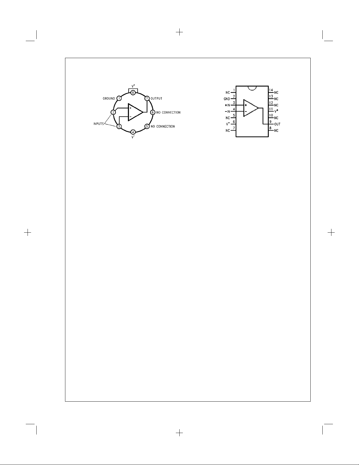
Schematic and Connection Diagrams (Continued)
Metal Can Package
Pin 4 is connected to case.
Top View
Order Number LM710AMH/883
LM710H/883 or LM710CH
See NS Package Number H08C
* Also available per JM38510/10301
DS010410-2
*
, LM710H,
Dual-In-Line Package
DS010410-3
Top View
Order Number
LM710AMJ/883
*
or LM710CN
See NS Package Number N14A or J14A
www.national.com 2
PrintDate=1997/05/16 PrintTime=10:46:07 7730 ds010410 Rev. No. 1 Proof 2
Absolute Maximum Ratings (Note *NO
TARGET FOR FNXref NS0053*)
If Military/Aerospace specified devices are required,
please contact the National Semiconductor Sales Office/
Distributors for availability and specifications.
Positive Supply Voltage +14V
Negative Supply Voltage −7V
Peak Output Current 10 mA
Output Short Circuit Duration 10 seconds
Differential Input Voltage
Input Voltage
±
±
Power Dissipation
TO-99 (Note 1) 700 mW
Plastic Dual-In-Line Package
(Note 2) 950 mW
Operating Temperature Range
LM710 −55˚C to +125˚C
LM710C 0˚C to +70˚C
Storage Temperature Range −65˚C to +150˚C
Lead Temperature
5V
(Soldering, 10 sec.) 260˚C
7V
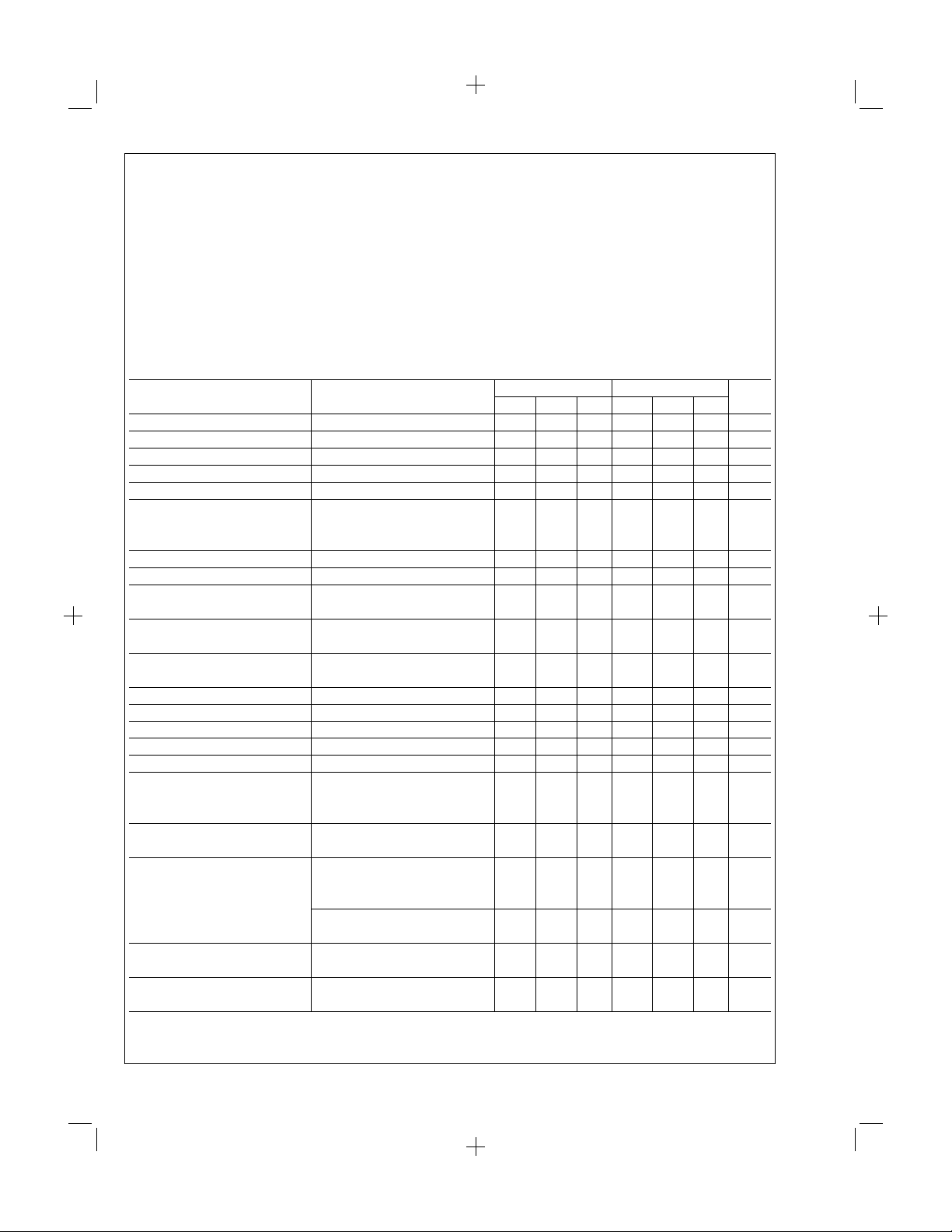
Electrical Characteristics (Note 3)
Parameter Conditions LM710 LM710C Units
Min Typ Max Min Typ Max
1.4V, T
0, T
A
≤ T
A
CM
=
CM
MAX
MAX
A
25˚C
=
=
=
Input Offset Voltage R
Input Offset Current V
Input Bias Current T
Voltage Gain T
Output Resistance T
Output Sink Current V
Response Time T
Input Offset Voltage R
Average Temperature Coefficient T
of Input Offset Voltage R
Input Offset Current T
≤ 200Ω,V
S
=
OUT
=
25˚C 13 20 16 25 µA
A
=
25˚C 1250 1700 1000 1500
A
=
25˚C 200 200 Ω
A
=
OUT
∆V
≥ 5 mV 2.0 2.5 mA
IN
∆V
≥ 10 mV 1.6 2.5 mA
IN
=
25˚C (Note 4) 40 40 ns
A
≤ 200Ω,V
S
≤ TA≤ T
MIN
≤ 50Ω
S
=
T
A
=
T
T
A
Average Temperature Coefficient 25˚C ≤ T
of Input Offset Current T
Input Bias Current T
Input Voltage Range V
Common-Mode Rejection Ratio R
≤ TA≤ 25˚C 15 75 24 100 nA/˚C
MIN
=
T
A
−
=
−7V
≤ 200Ω 80 100 70 98 dB
S
A MAX
A MIN
MIN
Differential Input Voltage Range
Voltage Gain 1000 800 V/V
Positive Output Level −5 mA ≤ I
V
≥ 5 mV 2.5 3.2 4.0 V
IN
V
≥ 10 mV 2.5 3.2 4.0 V
Negative Output Level V
Output Sink Current V
IN
≥ 5 mV −1.0 −0.5 0 V
IN
V
≥ 10 mV −1.0 −0.5 0 V
IN
≥ 5 mV, V
IN
=
T
A
=
T
A
V
≥ 10 mV, V
IN
0˚C ≤ T
Positive Supply Current V
Negative Supply Current V
≥ 5 mV 5.2 9.0 mA
IN
V
≥ 10 mV 5.2 9.0 mA
IN
≥ 5 mV 4.6 7.0 mA
IN
V
≥ 10 mV 4.6 7.0 mA
IN
≤ 0
OUT
OUT
125˚C 0.5 1.7 mA
−55˚C 1.0 2.3 mA
OUT
≤ +70˚C
A
=
0V, T
25˚C 0.6 2.0 1.6 5.0 mV
A
25˚C 0.75 3.0 1.8 5.0 µA
0V 3.0 6.5 mV
3.0 10 5.0 20 µV/˚C
0.25 3.0 7.5 µA
1.8 7.0 7.5 µA
5.0 25 15 50 nA/˚C
27 45 25 40 µA
±
5.0
±
5.0
=
0
=
0 0.5 mA
±
5.0 V
±
5.0 V
3 www.national.com
PrintDate=1997/05/16 PrintTime=10:46:10 7730 ds010410 Rev. No. 1 Proof 3
 Loading...