

NSC LM675T Datasheet
LM675
Power Operational Amplifier
General Description
The LM675 is a monolithic power operational amplifier featuring widebandwidth and low input offset voltage, making it
equally suitable for AC and DC applications.
The LM675 iscapable of delivering outputcurrents in excess
of 3 amps,operating at supply voltages of up to 60V.The device overload protection consists of both internal current limiting and thermal shutdown. The amplifier is also internally
compensated for gains of 10 or greater.
Features
n 3A current capability
n A
typically 90 dB
VO
n 5.5 MHz gain bandwidth product
n 8 V/µs slew rate
n Wide power bandwidth 70 kHz
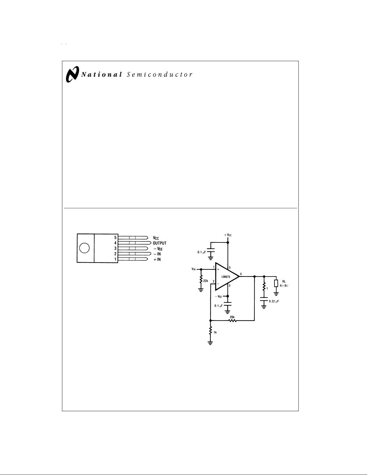
Connection Diagram Typical Applications
n 1 mV typical offset voltage
n Short circuit protection
n Thermal protection with parole circuit (100%tested)
n 16V–60V supply range
n Wide common mode range
n Internal output protection diodes
n 90 dB ripple rejection
n Plastic power package TO-220
Applications
n High performance power op amp
n Bridge amplifiers
n Motor speed controls
n Servo amplifiers
n Instrument systems
LM675 Power Operational Amplifier
May 1999
TO-220 Power Package (T)
*
The tab is internally connected to pin 3 (−VEE)
Front View
Order Number LM675T
See NS Package T05D
Non-Inverting Amplifier
DS006739-1
DS006739-2
© 1999 National Semiconductor Corporation DS006739 www.national.com
Absolute Maximum Ratings (Note 1)
If Military/Aerospace specified devices are required,
please contact theNational Semiconductor Sales Office/
Distributors for availability and specifications.
Supply Voltage
Input Voltage −V
±
30V
to V
EE
Storage Temperature −65˚C to +150˚C
Junction Temperature 150˚C
Power Dissipation (Note 2) 30W
Lead Temperature
(Soldering, 10 seconds) 260˚C
ESD rating to be determined.
CC
Operating Temperature 0˚C to +70˚C
Electrical Characteristics
=
V
S
Supply Current P
Input Offset Voltage V
Input Bias Current V
Input Offset Current V
Open Loop Gain R
PSRR ∆V
CMRR V
Output Voltage Swing R
Offset Voltage Drift Versus Temperature R
Offset Voltage Drift Versus Output Power 25 µV/W
Output Power THD=1%,f
Gain Bandwidth Product f
Max Slew Rate 8 V/µs
Input Common Mode Range
Note 1: AbsoluteMaximumRatingsindicatelimitsbeyondwhich damage to the device may occur. Operating Ratings indicate conditions for which the device is functional, but do not guarantee specific performance limits. Electrical Characteristics state DC and AC electrical specifications under particular test conditions which guarantee specific performance limits. This assumes that the device is within the Operating Ratings. Specifications are not guaranteed for parameters where no limit is
given, however, the typical value is a good indication of device performance.
Note 2: Assumes T
±
25V, T
=
25˚C unless otherwise specified.
A
Parameter Conditions Typical Tested Limit Units
=
0W 18 50 (max) mA
OUT
=
0V 1 10 (max) mV
CM
=
0V 0.2 2 (max) µA
CM
=
0V 50 500 (max) nA
CM
=
∞
Ω 90 70 (min) dB
L
=
±
5V 90 70 (min) dB
S
=
±
20V 90 70 (min) dB
IN
=
8Ω
L
<
100 kΩ 25 µV/˚C
S
=
1 kHz, R
20 kHz, A
O
VCL
=
O
equal to 70˚C. For operation at higher tab temperatures, the LM675 must be derated based on a maximum junction temperature of 150˚C.
A
=
8Ω 25 20 W
L
=
1000 5.5 MHz
±
21
±
22
±
18 (min) V
±
20 (min) V
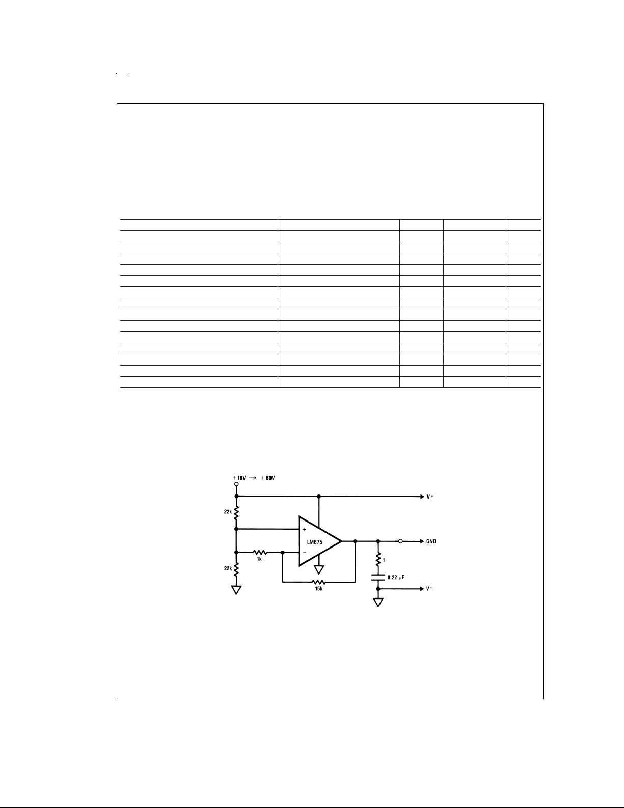
Typical Applications
Generating a Split Supply From a Single Supply
=
→
±
V
S
www.national.com 2
±
8V
30V
DS006739-3
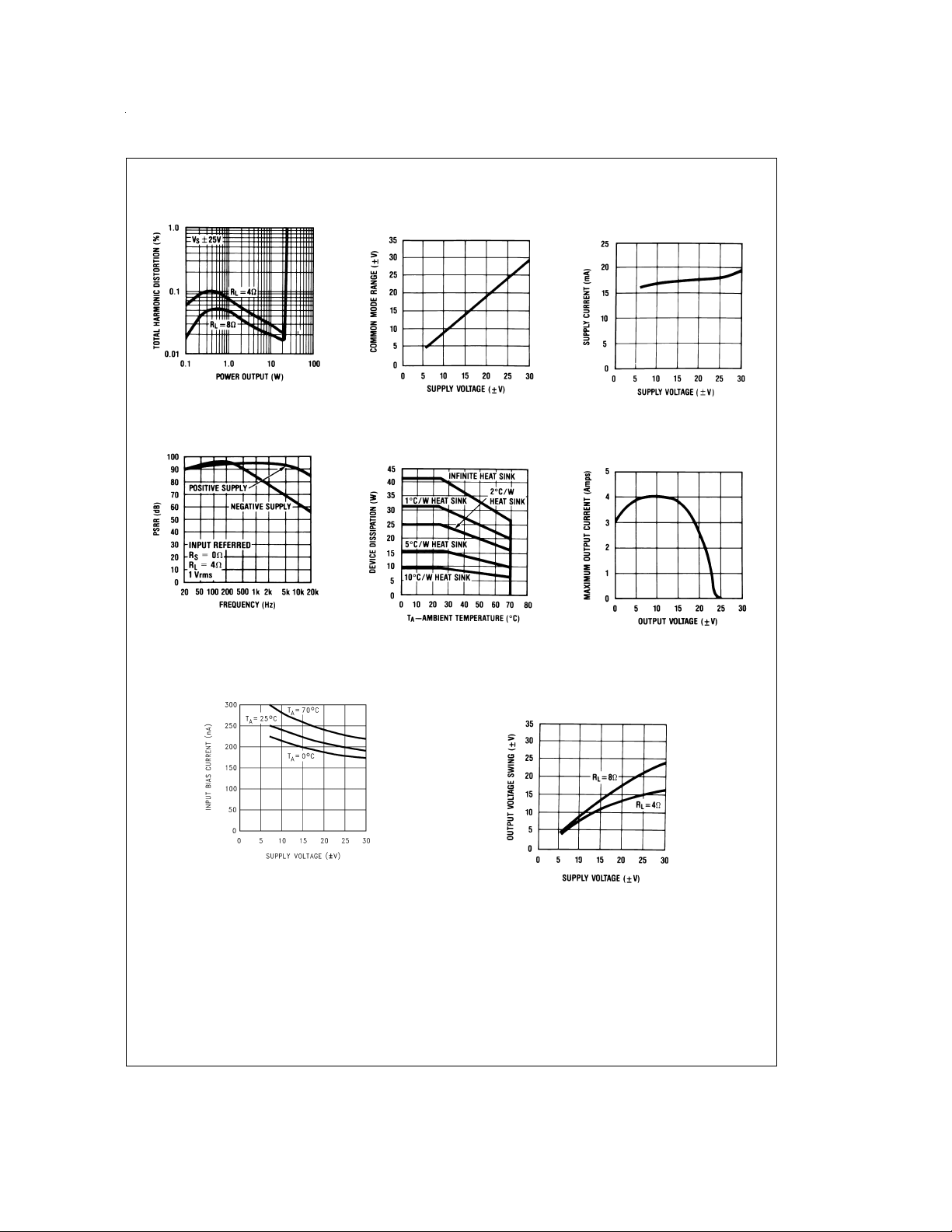
Typical Performance Characteristics
THD vs Power Output
PSRR vs Frequency
DS006739-10
DS006739-13
Input Common Mode
Range vs Supply Voltage
Device Dissipation vs
Ambient Temperature
†
θ INTERFACE=1˚ C/W
See Application Hints.
†
DS006739-11
DS006739-14
Supply Current vs
Supply Voltage
Current Limit vs
Output Voltage
=
±
*
V
S
*
25V
DS006739-12
DS006739-15
IBvs Supply Voltage
Output Voltage
Swing vs Supply Voltage
DS006739-16
DS006739-17
www.national.com3
 Loading...