

NSC LM64CILQX-F, LM64CILQ-F Datasheet
December 2003
LM64
±
1˚C Remote Diode Temperature Sensor with PWM Fan
Control and 5 GPIO’s
LM64
±
1˚C Remote Diode Temperature Sensor with PWM Fan Control and 5 GPIO’s
General Description
The LM64 is a remote diode temperature sensor with PWM
fan control. The LM64 accurately measures its own temperature and that of a remote diode. The LM64 remote temperature accuracy is factory trimmed for a MMBT3904 diodeconnected transistor with a 16˚C offset for high
temperatures. T
The LM64 features a PWM, open-drain, fan control output, 5
GPIO (General Purpose Input/Output) and 5 GPD (General
Purpose Default) pins. The 8-step Lookup Table allows for a
non-linear fan speed vs. temperature transfer function often
used to quiet acoustic fan noise.
ACTUAL DIODE JUNCTION
=T
LM64
+ 16˚C
Features
n Accurately senses remote and local diode temperatures
n Integrated PWM fan speed control output
n Programmable 8-step Lookup Table for quieting fans
n ALERT and T_Crit open-drain outputs
n Tachometer input for measuring fan RPM
n 10 bit plus sign remote diode temperature data format,
with 0.125˚C resolution
n SMBus 2.0 compatible interface, supports TIMEOUT
n 5 General Purpose Input/Output pins
n 5 General Purpose Default input pins
n 24-pin LLP package
Key Specifications
n Remote Diode Temperature Accuracy (includes
quantization error)
Ambient Temp Diode Temp Max Error
±
30˚C to 50˚C 120˚C to 140˚C
0˚C to 85˚C 25˚C to 140˚C
n Local Temp Accuracy (includes quantization error)
Ambient Temp Max Error
25˚C to 125˚C
n Power Supply Requirements
Supply DC Voltage 3.0 V to 3.6 V
Supply DC Current 1.1 mA (typ)
1.0˚C (max)
±
3.0˚C (max)
±
3.0˚C (max)
Applications
n Computer Processor Thermal Management
n Graphics Processor Thermal Management
n Voltage Regulator Modules
n Electronic Instrumentation
n Power Supplies
n Projectors
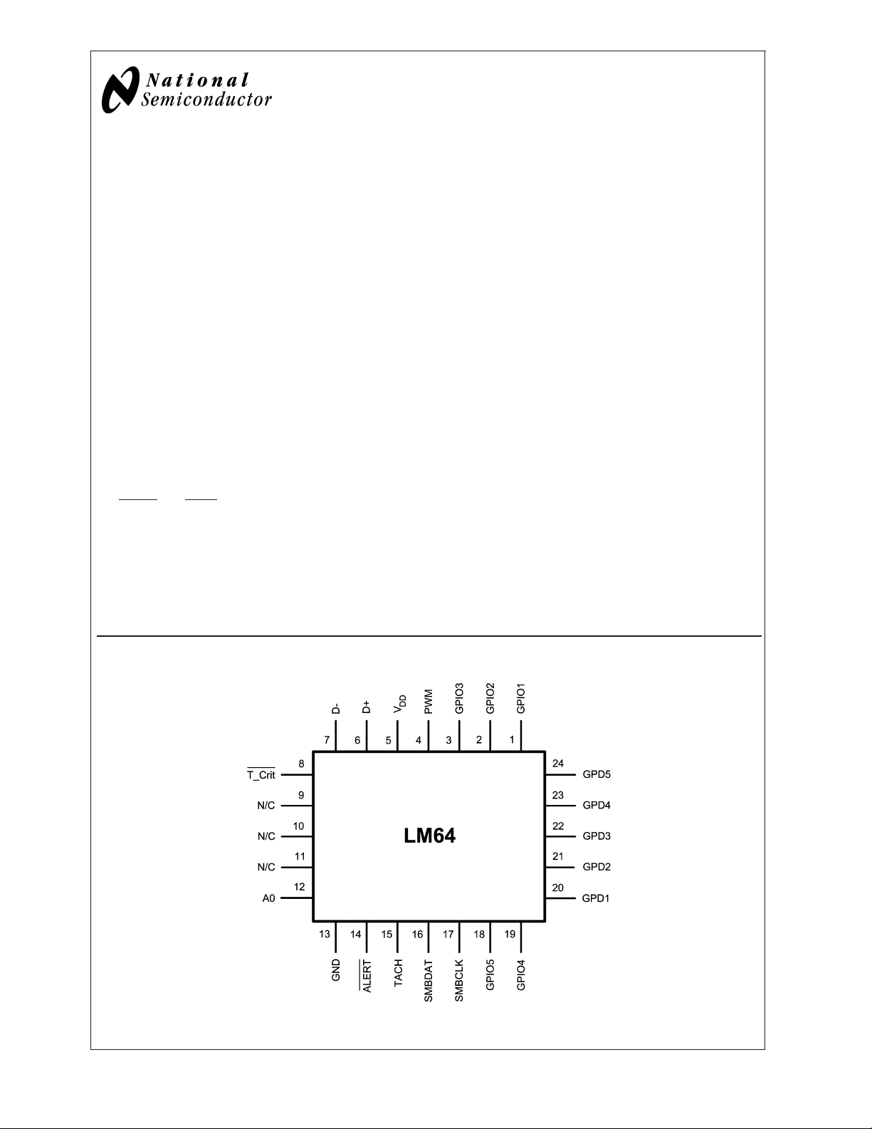
Connection Diagram
20065501
© 2003 National Semiconductor Corporation DS200655 www.national.com
Pin Descriptions
LM64
Pin Name Input/Output Function and Connection
1 GPIO1
2 GPIO2
3 GPIO3
4 PWM
5V
DD
Digital Input/
Open-Drain Output
Digital Input/
Open-Drain Output
Digital Input/
Open-Drain Output
Open-Drain
Digital Output
Power Supply Input
General Purpose Open-Drain Digital Output or Digital Input. Typical pull-up
resistor is 10 kΩ to V
.
DD
General Purpose Open-Drain Digital Output or Digital Input. Typical pull-up
resistor is 10 kΩ to VDD.
General Purpose Open-Drain Digital Output or Digital Input. Typical pull-up
resistor is 10 kΩ to V
.
DD
Open-Drain Digital Output. Connect to fan drive circuitry. The power-on
default for this pin is low (pin 4 pulled to ground).
Connect to a low-noise +3.3
±
0.3 VDC power supply, and bypass to GND
with a 0.1 µF ceramic capacitor in parallel with a 100 pF ceramic capacitor.
A bulk capacitance of 10 µF needs to be in the vicinity of the LM64’s V
pin.
6 D+ Analog Input
7 D- Analog Input
8 T_Crit
Open-Drain
Digital Output
Connect to the anode (positive side) of the remote diode. A 2.2 nF ceramic
capacitor must be connected between pins 6 and 7.
Connect to the cathode (negative side) of the remote diode. A 2.2 nF
ceramic capacitor must be connected between pins 6 and 7.
Open-Drain Digital Output. Typical pull-up resistor is 3 kΩ to V
9 N/C N/A No Connection.
10 N/C N/A No Connection.
11 N/C N/A No Connection.
12 A0 Digital Input
SMBus Address Select pin. If High, the SMBus address is 0x4E or, if Low,
the SMBus address is 0x18. Typical pull-up resistor is 10 kΩ to V
13 GND Ground This is the analog and digital ground return.
14 ALERT
Open-Drain
Digital Output
15 TACH Digital Input
16 SMBDAT
Digital Input/
Open-Drain Output
This pin is an open-drain ALERT Output. Typical pull-up resistor is 3 kΩ to
.
V
DD
This pin is a digital tachometer input. Typical pull-up resistor is 3 kΩ to
.
V
DD
This is the bi-directional SMBus data line. Typical pull-up resistor is 1.5 kΩ
.
to V
DD
17 SMBCLK Digital Input This is the SMBus clock input. Typical pull-up resistor is 1.5 kΩ to V
18 GPIO5
19 GPIO4
Digital Input/
Open-Drain Output
Digital Input/
Open-Drain Output
20 GPD1 Digital Input
21 GPD2 Digital Input
22 GPD3 Digital Input
23 GPD4 Digital Input
24 GPD5 Digital Input
General Purpose Open-Drain Digital Output or Digital Input. Typical pull-up
resistor is 10 kΩ to V
.
DD
General Purpose Open-Drain Digital Output or Digital Input. Typical pull-up
resistor is 10 kΩ to V
.
DD
General Purpose Default Input Pin. Typical pull-up resistor is 10 kΩ to V
Always connect to a logical High or Low level.
General Purpose Default Input Pin. Typical pull-up resistor is 10 kΩ to VDD.
Always connect to a logical High or Low level.
General Purpose Default Input Pin. Typical pull-up resistor is 10 kΩ to V
Always connect to a logical High or Low level.
General Purpose Default Input Pin. Typical pull-up resistor is 10 kΩ to VDD.
Always connect to a logical High or Low level.
General Purpose Default Input Pin. Typical pull-up resistor is 10 kΩ to V
Always connect to a logical High or Low level.
DD
.
DD
.
DD
.
DD
.
DD
.
DD
.
DD
www.national.com 2
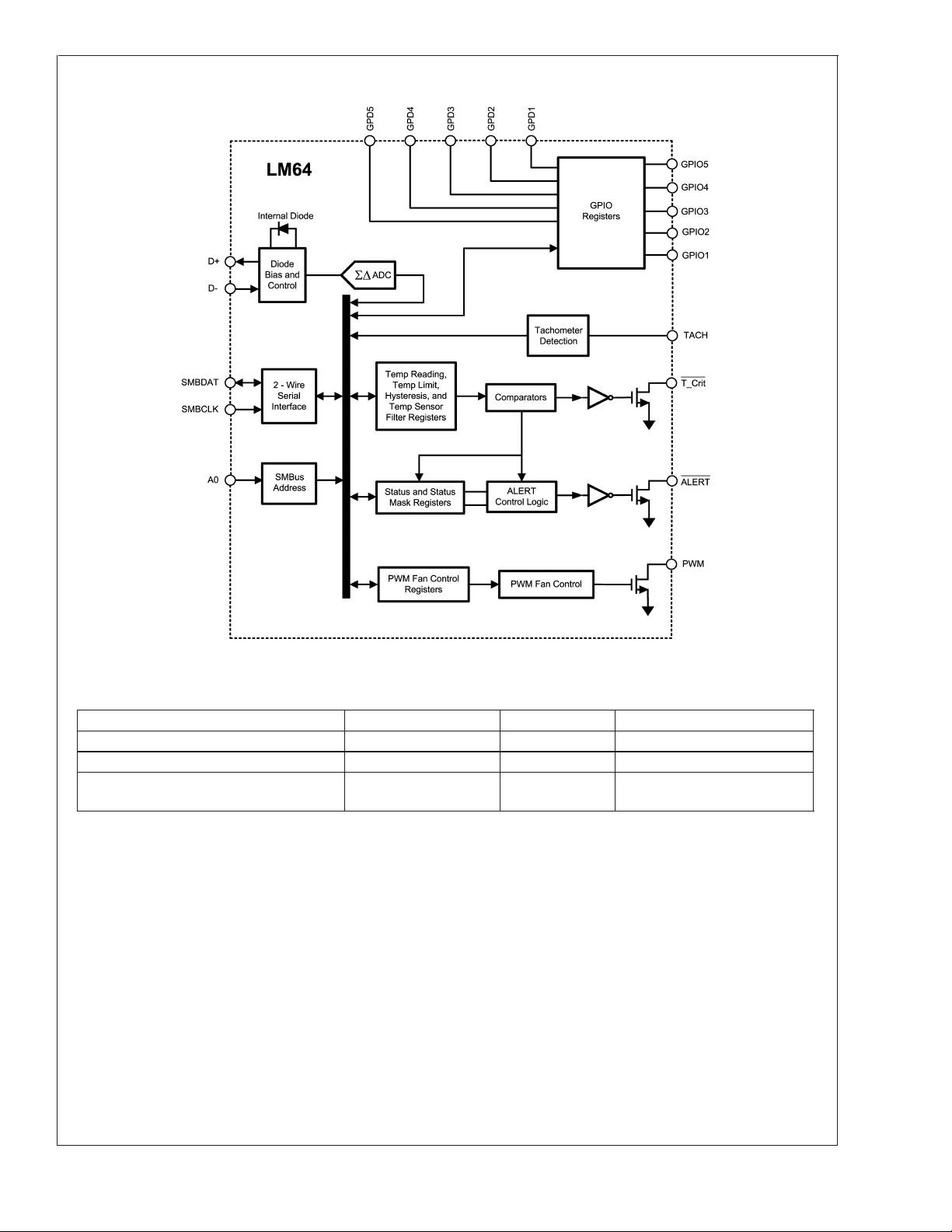
Simplified Block Diagram
LM64
Ordering Information
Part Description Order Number Top Mark Transport Media
LM64 24-pin LLP LM64CILQ-F 64CILQF 1000 Units in Tape and Reel
LM64 24-pin LLP LM64CILQX-F 64CILQF 4500 Units in Tape and Reel
LM64 Evaluation Board
With Software and Manual
20065502
LM64EVAL N/A Packaged
www.national.com3
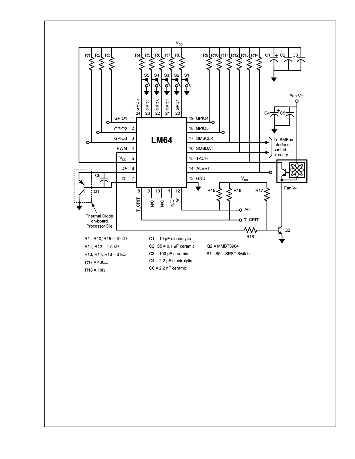
Typical Application
LM64
www.national.com 4
20065503
LM64
Absolute Maximum Ratings (Notes 1,
2)
Supply Voltage, V
DD
Voltage on SMBDAT, SMBCLK,
ALERT, T_Crit, PWM Pins −0.5 V to 6.0 V
Voltage on Other Pins −0.3 V to (V
Input Current, D− Pin
−0.3 V to 6.0 V
+0.3V)
DD
±
1mA
ESD Susceptibility (Note 4)
Human Body Model 2000 V
Machine Model 200 V
SMT Soldering Information
See National Semiconductor Application Note AN-1187,
"Leadless Leadframe Package" for information on SMT
Assembly using LLP Packages. This is available at
http://www.national.com/an/AN/AN-1187.pdf.
Input Current at All Other Pins (Note 3) 5 mA
Package Input Current (Note 3) 30 mA
Package Power Dissipation (Note 5)
SMBDAT, ALERT, T_Crit, PWM pins
Output Sink Current 10 mA
Storage Temperature −65˚C to +150˚C
Operating Ratings (Notes 1, 2)
LM64 Operating Temperature Range 0˚C ≤ T
Remote Diode Temperature Range 25˚C ≤ T
Electrical Characteristics T
MIN
≤ +85˚C
A
≤ +140˚C
D
≤ TA≤ T
MAX
Supply Voltage Range (VDD) +3.0 V to +3.6 V
DC Electrical Characteristics
TEMPERATURE-TO-DIGITAL CONVERTER CHARACTERISTICS The following specifications apply for VDD= 3.0 VDC to
3.6 VDC, and all analog source impedance R
T
A=TMIN
to T
; all other limits TA= +25˚C.
MAX
Parameter Conditions
Temperature Error using a diode-connected
MMBT3904 transistor. T
is the Remote
D
Diode Junction Temperature.
T
D=TLM64
+ 16˚C
Temperature Error Using the Local Diode T
Remote Diode Resolution 11 Bits
Local Diode Resolution 8 Bits
Conversion Time of All Temperatures Fastest Setting 31.25 34.4 ms (max)
D− Source Voltage 0.7 V
Diode Source Current
=50Ω unless otherwise specified in the conditions. Boldface limits apply for
S
= +30˚C to
T
A
+50˚C
T
= +0˚C to
A
+85˚C
= +25˚C to +125˚C (Note 10)
A
TD= +120˚C to
+140˚C
TD= +25˚C to
+140˚C
Typical
(Note 7)
±
1
Limits
(Note 8)
±
1 ˚C (max)
±
3 ˚C (max)
±
3 ˚C (max)
Units
(Limits)
0.125 ˚C
1˚C
(V
D+−VD−
Current
) = +0.65 V; High
160
Low Current 13
315 µA (max)
110 µA (min)
20 µA (max)
7 µA (min)
Operating Electrical Characteristics
Parameter
ALERT, T_Crit and PWM Output Saturation
Voltage
Conditions
ALERT, T_Crit
I
I
OUT
OUT
4mA 6mA 0.4
6mA 0.55
PWM
Typ
(Note 7)
Power-On-Reset Threshold Voltage 2.4 V (max)
Supply Current (Note 9) SMBus Inactive, 16 Hz
Conversion Rate
1.1 2.0 mA (max)
STANDBY Mode 320 µA
Limits
(Note 8)
V (max)
1.8 V (min)
www.national.com5
Units
AC Electrical Characteristics
LM64
The following specifications apply for VDD= 3.0 VDC to 3.6 VDC, and all analog source impedance RS=50Ω unless other-
wise specified in the conditions. Boldface limits apply for T
A=TMIN
Symbol Parameter Conditions
to T
; all other limits TA= +25˚C.
MAX
Typical
(Note 7)
Limits
(Note 8)
TACHOMETER ACCURACY
Fan Control Accuracy
±
10 % (max)
Fan Full-Scale Count 65535 (max)
Fan Counter Clock Frequency 90 kHz
Fan Count Update Frequency 1.0 Hz
FAN PWM OUTPUT
Frequency Accuracy
±
10 % (max)
Digital Electrical Characteristics
Symbol Parameter Conditions
V
V
I
IH
I
IL
C
Logical High Input Voltage 2.1 V (min)
IH
Logical Low Input Voltage 0.8 V (max)
IL
Logical High Input Current VIN=V
DD
Logical Low Input Current VIN= GND −0.005 −10 µA (max)
Digital Input Capacitance 20 pF
IN
Typical
(Note 7)
0.005 +10 µA (max)
Limits
(Note 8)
Units
(Limit)
Units
(Limit)
SMBus Logical Electrical Characteristics
The following specifications apply for VDD= 3.0 VDC to 3.6 VDC, and all analog source impedance RS=50Ω unless other-
wise specified in the conditions. Boldface limits apply for T
A=TMIN
to T
Symbol Parameter Conditions
SMBDAT OPEN-DRAIN OUTPUT
V
I
OH
Logic Low Level Output Voltage IOL=4mA 0.4 V (max)
OL
High Level Output Current V
OUT=VDD
SMBDAT, SMBCLK INPUTS
V
V
V
HYST
Logical High Input Voltage 2.1 V (min)
IH
Logical Low Input Voltage 0.8 V (max)
IL
Logic Input Hysteresis Voltage 400 mV
; all other limits TA= +25˚C.
MAX
Typical
(Note 7)
0.03 10 µA (max)
Limits
(Note 8)
Units
(Limit)
www.national.com 6
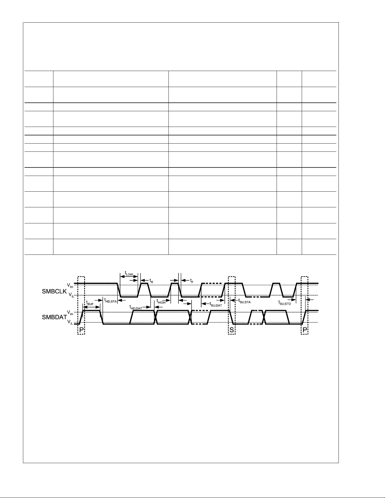
SMBus Digital Switching Characteristics
Unless otherwise noted, these specifications apply for VDD= +3.0 VDC to +3.6 VDC, CL(load capacitance) on output lines =
80 pF. Boldface limits apply for T
A=TJ;TMIN
≤ TA≤ T
switching characteristics of the LM64 fully meet or exceed the published specifications of the SMBus version 2.0. The following
parameters are the timing relationships between SMBCLK and SMBDAT signals related to the LM64. They adhere to but are
not necessarily the same as the SMBus bus specifications.
Symbol Parameter Conditions
f
SMB
t
LOW
t
HIGH
t
R
t
F
t
OF
t
TIMEOUT
SMBus Clock Frequency 10
SMBus Clock Low Time From V
SMBus Clock High Time From V
SMBus Rise Time (Note 11) 1 µs (max)
SMBus Fall Time (Note 12) 0.3 µs (max)
Output Fall Time CL= 400 pF, IO=3mA 250 ns (max)
SMBData and SMBCLK Time Low for Reset
of Serial Interface See (Note 13)
t
SU:DAT
t
HD:DAT
t
HD:STA
Data In Setup Time to SMBCLK High 250 ns (min)
Data Out Hold Time after SMBCLK Low 300
Hold Time after (Repeated) Start Condition.
After this period the first clock is generated.
t
SU:STO
Stop Condition SMBCLK High to SMBDAT
Low (Stop Condition Setup)
t
SU:STA
SMBus Repeated Start-Condition Setup Time,
SMBCLK High to SMBDAT Low
t
BUF
SMBus Free Time between Stop and Start
Conditions
; all other limits TA=TJ= +25˚C, unless otherwise noted. The
MAX
Limits
(Note 8)
100
IN(0) max
IN(1) min
to V
to V
IN(0) max
IN(1) min
4.7 µs (min)
4.0
50
25
35
930
4.0 µs (min)
100 ns (min)
4.7 µs (min)
4.7 µs (min)
Units
(Limit)
kHz (min)
kHz (max)
µs (min)
µs (max)
ms (min)
ms (max)
ns (min)
ns (max)
LM64
FIGURE 1. SMBus Timing Diagram for SMBCLK and SMBDAT Signals
20065504
www.national.com7
Notes
LM64
Note 1: Absolute Maximum Ratings indicate limits beyond which damage to the device may occur. Operating Ratings indicate conditions for which the device is
functional, but do not guarantee performance limits. For guaranteed specifications and test conditions, see the Electrical Characteristics. The guaranteed
specifications apply only for the test conditions listed. Some performance characteristics may degrade when the device is not operated under the listed test
conditions.
Note 2: All voltages are measured with respect to GND, unless otherwise noted.
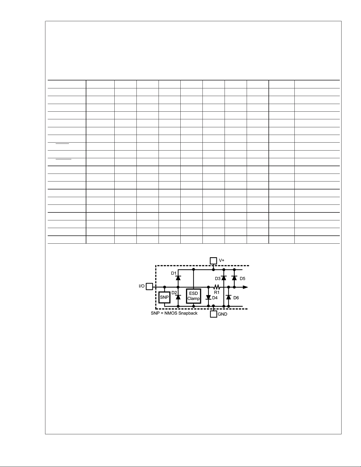
Note 3: When the input voltage (V
components and/or ESD protection circuitry are shown in the table below, for the LM64’s pins, by an "X" when it exists. Care should be taken not to forward bias
the parasitic diode, D1, present on pins D+ and D−. Doing so by more than 50 mV may corrupt temperature measurements.
) at any pin exceeds the power supplies (V
IN
IN
<
GND or V
>
V+), the current at that pin should be limited to 5 mA. Parasitic
IN
Pin Name PIN
#
D1 D2 D3 D4 D5 D6 R1 SNP ESD CLAMP
GPIO1 1 X X X
GPIO2 2 X X X
GPIO3 3 X X X
PWM 4 X X X
V
DD
5 X
D+ 6 XX XXX X
D− 7 XX XXX X
T_Crit
8X XXX
A0 12 X
ALERT
14 X X X X
TACH 15 X X X
SMBDAT 16 X X X
SMBCLK 17 X
GPIO5 18 X X X
GPIO4 19 X X X
GPD1 20 X
GPD2 21 X
GPD3 22 X
GPD4 23 X
GPD5 24 X
20065505
FIGURE 2. ESD Protection Input Structure
Note 4: Human body model, 100 pF discharged through a 1.5 kΩ resistor. Machine model, 200 pF discharged directly into each pin. See Figure 2 above for the ESD
Protection Input Structure.
Note 5: See the National Semiconductor Application Note AN-1187 for Thermal Resistance Junction-to-Ambient Temperature.
Note 6: See the National Semiconductor Application Note AN-1187 for recommendations on SMT assembly using the LLP packages.
Note 7: “Typicals” are at T
Note 8: Limits are guaranteed to National’s AOQL (Average Outgoing Quality Level).
Note 9: The supply current will not increase substantially with an SMBus transaction.
Note 10: Local temperature accuracy does not include the effects of self-heating. The rise in temperature due to self-heating is the product of the internal power
dissipation of the LM64 and the thermal resistance. See (Note 5) for the thermal resistance to be used in the self-heating calculation.
Note 11: The output rise time is measured from (V
Note 12: The output fall time is measured from (V
Note 13: Holding the SMBData and/or SMBCLK lines Low for a time interval greater than t
SMBDAT and SMBCLK pins to a high impedance state.
www.national.com 8
= 25˚C and represent most likely parametric norm. They are to be used as general reference values not for critical design calculations.
A
IL max
IH min
- 0.15 V) to (V
+ 0.15 V) to (V
IH min
IL min
+ 0.15 V).
- 0.15 V).
will reset the LM64’s SMBus state machine, therefore setting
TIMEOUT
1.0 Functional Description
The LM64 Remote Diode Temperature Sensor with Integrated Fan Control incorporates a ∆V
sensor using a Local or Remote diode and a 10-bit plus sign
∆Σ ADC (Delta-Sigma Analog-to-Digital Converter). The
pulse-width modulated (PWM) open-drain output, with a
pull-up resistor, can drive a switching transistor to modulate
the fan. The LM64 can measure the fan speed on the pulses
from the fan’s open-collector tachometer output, pulled up by
a 1.5 kΩ resistor to V
. The ALERT open-drain output will
DD
be pulled low under certain conditions descibed in the sections below. The T_Crit open-drain output will be pulled low
when the T_Crit setpoint temperature limit is exceeded. This
behaves as a typical comparator function without any latching.
The LM64’s two-wire interface is compatible with the SMBus
Specification 2.0 . For more information the reader is directed to www.smbus.org.
In the LM64, digital comparators are used to compare the
measured Local Temperature (LT) to the Local High Setpoint
user-programmable temperature limit register. The measured Remote Temperature (RT) is digitally compared to the
Remote High Setpoint (RHS), the Remote Low Setpoint
(RLS), and the Remote T_CRIT Setpoint (RCS) userprogrammable temperature limits. An ALERT output will occur when the measured temperature is: (1) higher than either
the High Setpoint or the T_CRIT Setpoint, or (2) lower than
the Low Setpoint. The ALERT Mask register allows the user
to prevent the generation of these ALERT outputs.
The temperature hysteresis is set by the value placed in the
Hysteresis Register (TH).
The LM64 may be placed in a low power Standby mode by
setting the Standby bit found in the Configuration Register. In
the Standby mode continuous conversions are stopped. In
Standby mode the user may choose to allow the PWM
output signal to continue, or not, by programming the PWM
Disable in Standby bit in the Configuration Register.
The Local Temperature reading and setpoint data registers
are 8-bits wide. The format of the 11-bit remote temperature
data is a 16-bit left justified word. Two 8-bit registers, high
and low bytes, are provided for each setpoint as well as the
temperature reading. Two Remote Temperature Offset
(RTO) Registers: High Byte and Low Byte (RTOHB and
RTOLB) may be used to correct the temperature readings by
adding or subtracting a fixed value based on a different
non-ideality factor of the thermal diode if different from the
graphics processor thermal diode. See Section 4.1 Thermal
Diode Non-Ideality.
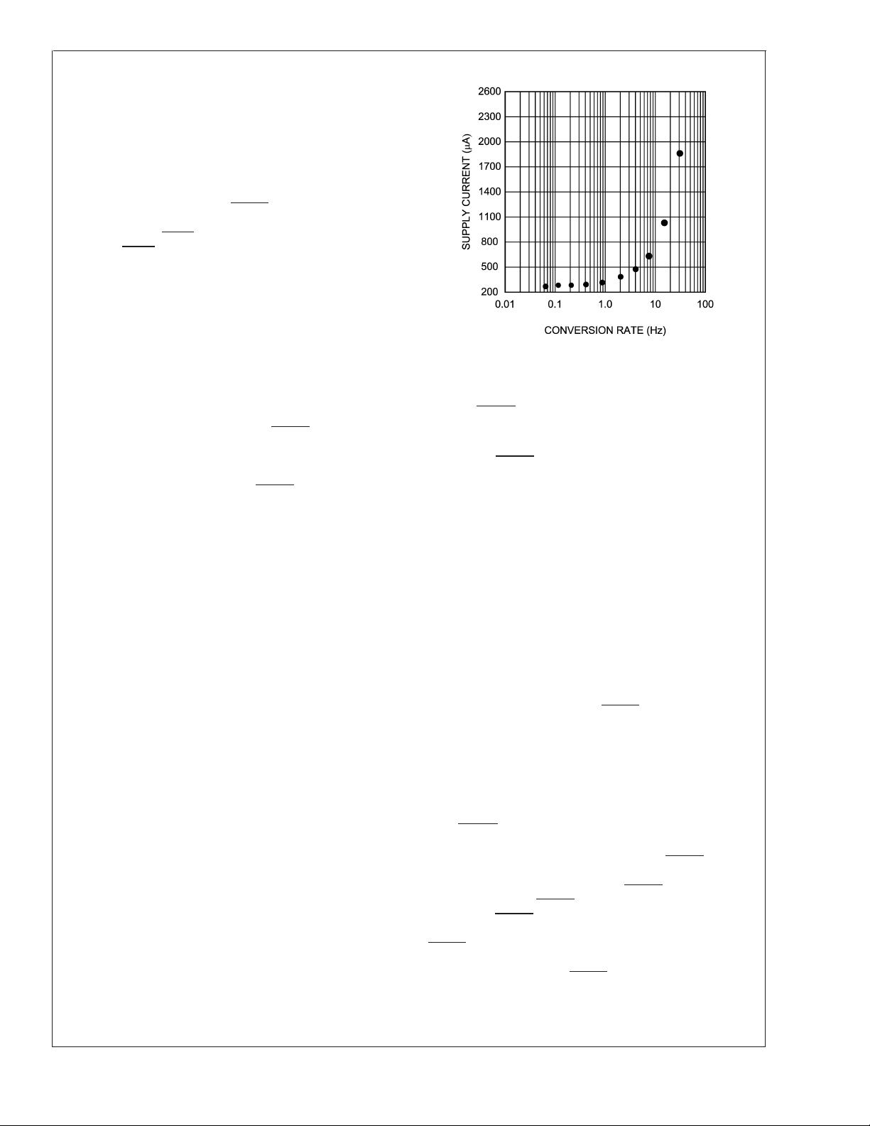
1.1 CONVERSION SEQUENCE
The LM64 takes approximately 31.25 ms to convert the
Local Temperature (LT), Remote Temperature (RT), and to
update all of its registers. The Conversion Rate may be
modified using the Conversion Rate Register. When the
conversion rate is modified a delay is inserted between
conversions, the actual conversion time remains at
31.25 ms. Different Conversion Rates will cause the LM64 to
draw different amounts of supply current as shown in Figure
3.
-based temperature
BE
LM64
20065506
FIGURE 3. Supply Current vs Conversion Rate
1.2 THE ALERT OUTPUT
When the ALERT Mask bit in the Configuration register is
written as zero the ALERT interrupts are enabled.
The LM64’s ALERT pin is versatile and can produce three
different methods of use to best serve the system designer:
(1) as a temperature comparator (2) as a temperature-based
interrupt flag, and (3) as part of an SMBus ALERT System.
The three methods of use are further described below. The
ALERT and interrupt methods are different only in how the
user interacts with the LM64.
The remote temperature (RT) reading is associated with a
T_CRIT Setpoint Register, and both local and remote temperature (LT and RT) readings are associated with a HIGH
setpoint register (LHS and RHS). The RT is also associated
with a LOW setpoint register (RLS). At the end of every
temperature reading a digital comparison determines
whether that reading is above its HIGH or T_CRIT setpoint or
below its LOW setpoint. If so, the corresponding bit in the
ALERT Status Register is set. If the ALERT mask bit is low,
any bit set in the ALERT Status Register, with the exception
of Busy or Open, will cause the ALERT output to be pulled
low. Any temperature conversion that is out of the limits
defined in the temperature setpoint registers will trigger an
ALERT. Additionally, the ALERT Mask Bit must be cleared to
trigger an ALERT in all modes.
The three different ALERT modes will be discussed in the
following sections.
1.2.1 ALERT Output as a Temperature Comparator
When the LM64 is used in a system in which does not
require temperature-based interrupts, the ALERT output
could be used as a temperature comparator. In this mode,
once the condition that triggered the ALERT to go low is no
longer present, the ALERT is negated (Figure 4). For example, if the ALERT output was activated by the comparison
of LT>LHS, when this condition is no longer true, the
ALERT will return HIGH. This mode allows operation without
software intervention, once all registers are configured during set-up. In order for the ALERT to be used as a temperature comparator, the Comparator Mode bit in the Remote
Diode Temperature Filter and Comparator Mode Register
must be asserted. This is not the power-on default state.
www.national.com9
 Loading...