NSC LM6125H-883, LM6125MD8 Datasheet

LM6125/LM6225/LM6325
High Speed Buffer
General Description
The LM6125 family of high speed unity gain buffers slew at
800 V/µsand have a small signal bandwidth of 50 MHz while
driving a 50Ω load. These buffers drive
±
300 mA peak and
do not oscillate while driving large capacitive loads. The
LM6125 contains unique features notfound inpower buffers;
these include current limit, thermal shutdown, electronic
shutdown, and an error flag that warns of fault conditions.
These buffers are built with National’s VIP
™
(Vertically Integrated PNP) process which provides fast PNP transistors
that are true complements to the already fast NPN devices.
This advanced junction-isolated process delivers high speed
performance without the need for complexand expensivedielectric isolation.
Features
n High slew rate: 800 V/µs
n High output current:
±
300 mA
n Stable with large capacitive loads
n Current and thermal limiting
n Electronic shutdown
n 5V to
±
15V operation guaranteed
n Fully specified to drive 50Ω lines
Applications
n Line Driving
n Radar
n Sonar
Simplified Schematic and Block Diagram
VIP™is a trademark of National Semiconductor Corporation.
DS009222-1
DS009222-2
Numbers in () are for 14–pin N DIP.
December 1994
LM6125/LM6225/LM6325 High Speed Buffer
© 1999 National Semiconductor Corporation DS009222 www.national.com

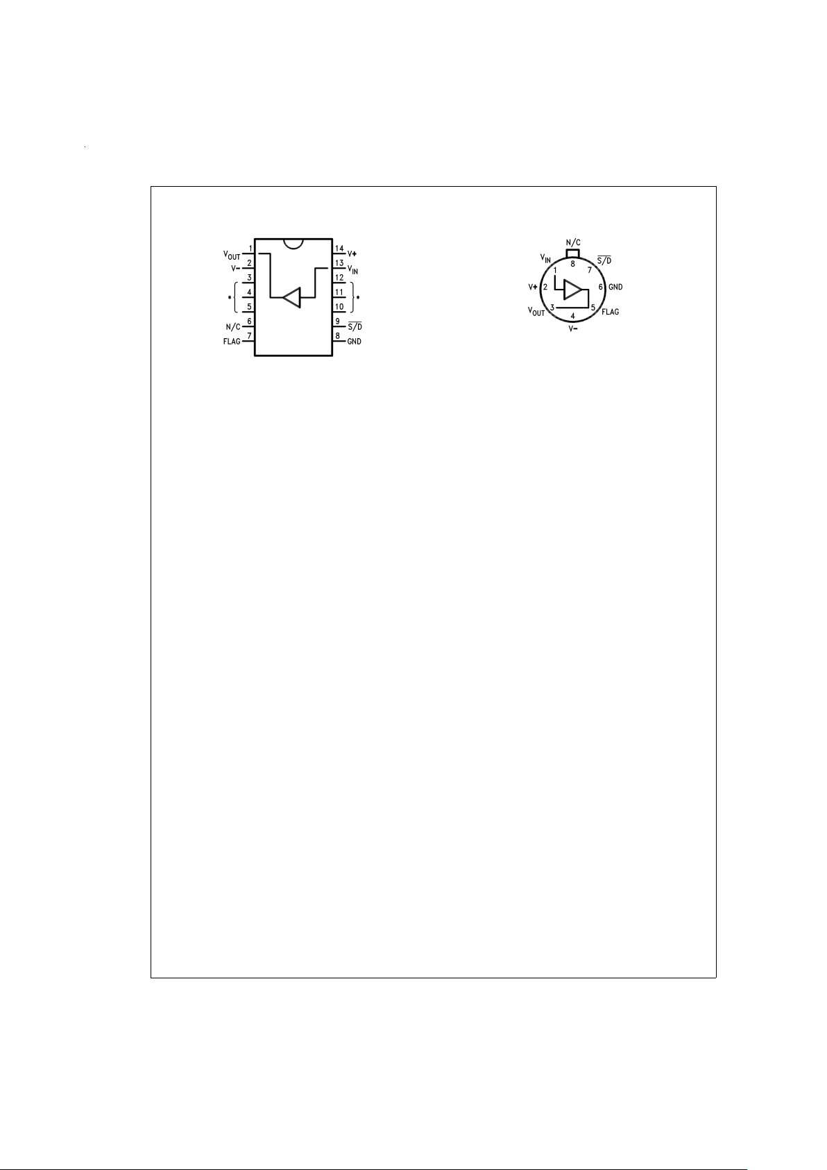
Pin Configurations
Note 1: Available per 5962-9081501
DS009222-3
*Heat sinking pins.
Internally connected to V−.
Order Number LM6225N
or LM6325N
See NS Package Number N14A
DS009222-4
Note: Pin 4 connected to case
Top View
Order Number LM6125H/883 (Note 1)
or LM6125H
See NS Package Number H08C
www.national.com 2

Absolute Maximum Ratings (Note 2)
If Military/Aerospace specified devices are required,
please contact the National Semiconductor Sales Office/
Distributors for availability and specifications.
Supply Voltage 36V (
±
18V)
Input to Output Voltage (Note 2)
±
7V
Input Voltage
±
Vsupply
Output Short-Circuit to GND
(Note 3) Continuous
Flag Output Voltage GND ≤ Vflag ≤ +Vsupply
Storage Temperature Range −65˚C to +150˚C
Lead Temperature
(Soldering, 10 seconds) 260˚C
ESD Tolerance (Note 9)
±
1500V
θ
JA
(Note 4)
H Package 150˚C/W
N Package 40˚C/W
Maximum Junction
Temperature (T
J
) 150˚C
Operating Temperature Range
LM6125 −55˚C to +125˚C
LM6225 −40˚C to +85˚C
LM6325 0˚C to +70˚C
Operating Supply Voltage Range 4.75V to
±
16V
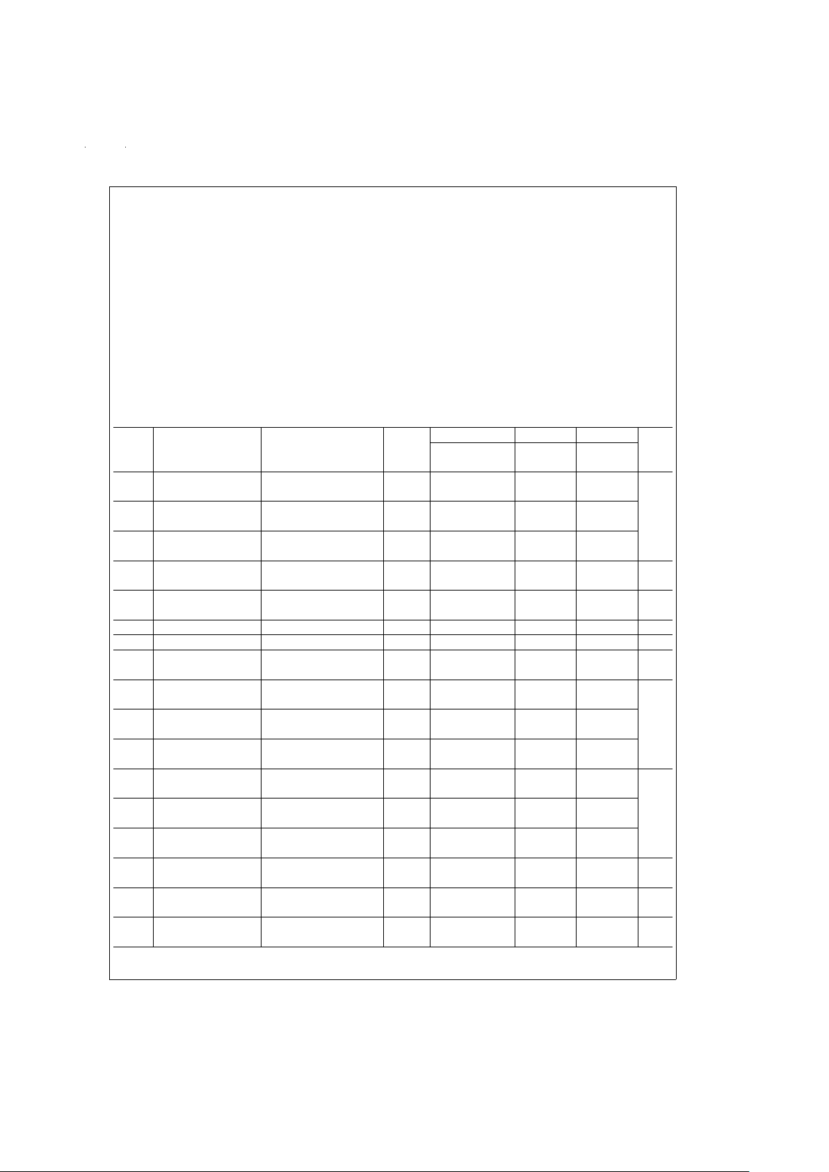
DC Electrical Characteristics
The following specifications apply for Supply Voltage
=
±
15V, V
CM
=
0, R
L
≥ 100 kΩ and R
S
=
50Ω unless otherwise noted.
Boldface limits apply for T
A
=
T
J
=
T
MIN
to T
MAX
; all other limits T
A
=
T
J
=
25˚C.
Symbol Parameter Conditions Typ LM6125 LM6225 LM6325 Units
Limit Limit Limit
(Notes 5, 10) (Note 5) (Note 5)
A
V1
Voltage Gain 1 R
L
=
1kΩ,V
IN
=
±
10V 0.990 0.980 0.980 0.970
0.970 0.950 0.950
A
V2
Voltage Gain 2 R
L
=
50Ω,V
IN
=
±
10V 0.900 0.860 0.860 0.850 V/V
0.800 0.820 0.820 Min
A
V3
Voltage Gain 3 R
L
=
50Ω,V+=5V 0.840 0.780 0.780 0.750
(Note 6) V
IN
=
2V
PP
(1.5 VPP) 0.750 0.700 0.700
V
OS
Offset Voltage R
L
=
1kΩ 15 30 30 50 mV
50 60 100 Max
I
B
Input Bias Current R
L
=
1kΩ,R
S
=
10 kΩ 14 45µA
777Max
R
IN
Input Resistance R
L
=
50Ω 5MΩ
C
IN
Input Capacitance 3.5 pF
R
O
Output Resistance I
OUT
=
±
10 mA 3 5 5 5 Ω
10 10 6 Max
I
S1
Supply Current 1 R
L
=
∞
15 18 18 20
20 20 22
I
S2
Supply Current 2 R
L
=
∞
,V+=5V 14 16 16 18 mA
18 18 20 Max
I
S/D
Supply Current R
L
=
∞
,V
±=±
15V 1.1 1.5 1.5 1.5
in Shutdown 2.0 2.0 2.0
V
O1
Output Swing 1 R
L
=
1kΩ 13.5 13.3 13.3 13.2
13 13 13
V
O2
Output Swing 2 R
L
=
100Ω 12.7 11.5 11.5 11
±
V
10 10 10 Min
V
O3
Output Swing 3 R
L
=
50Ω 12 11 11 10
999
V
O4
Output Swing 4 R
L
=
50Ω 1.8 1.6 1.6 1.6 V
PP
1.3 1.4 1.5 Min
PSRR Power Supply V+=5V (Note 6) 70 60 60 60 dB
Rejection Ratio 55 50 50 Min
V
OL
Flag Pin Output V
±=±
5V to±15V 300 300 340 mV
Low Voltage V
S/D
=
0V 400 400 400 Max
www.national.com3
 Loading...