

NSC LM6104M, LM6104MX Datasheet
TL/H/11979
LM6104 Quad Gray Scale Current Feedback Amplifier
June 1994
LM6104
Quad Gray Scale Current Feedback Amplifier
General Description
The LM6104 quad amplifier meets the requirements of battery operated liquid crystal displays by providing high speed
while maintaining low power consumption.
Combining this high speed with high integration, the
LM6104 conserves valuable board space in portable systems with a cost effective, surface mount quad package.
Built on National’s advanced high speed VIP
TM
(Vertically
Integrated PNP) process, the LM6104 current feedback architecture is easily compensated for speed and loading conditions. These features make the LM6104 ideal for buffering
grey levels in liquid crystal displays.
Features (Typical unless otherwise noted)
Y
Low power I
S
e
875 mA/amplifier
Y
Slew rate 100V/ms
Y
b
3dB bandwidth (R
F
e
1kX) 30 MHz
Y
High output drive
g
5V into 100X
Y
Wide operating range V
S
e
5V tog12V
Y
High integration Quad surface mount
Applications
Y
Grey level buffer for liquid crystal displays
Y
Column buffer for portable LCDs
Y
Video distribution amplifiers, video line drivers
Y
Hand-held, high speed signal conditioning
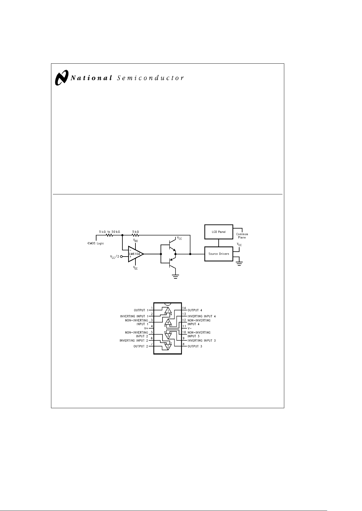
Typical Application
LCD Buffer Application for Grey Levels
TL/H/11979– 1
Connection Diagram
TL/H/11979– 2
Order Number LM6104M
See NS Package Number M14A
VIPTMis a trademark of National Semiconductor Corporation.
C
1995 National Semiconductor Corporation RRD-B30M115/Printed in U. S. A.
Absolute Maximum Ratings (Note 1)
If Military/Aerospace specified devices are required,
please contact the National Semiconductor Sales
Office/Distributors for availability and specifications.
Supply Voltage 24V
Differential Input Voltage
g
6V
Input Voltage
g
Supply Voltage
Inverting Input Current 15 mA
Soldering Information
Vapor Phase (60s) 215
§
C
Infrared (15s) 220
§
C
Storage Temperature Range
b
65§CsT
J
s
a
150§C
Maximum Junction Temperature 150§C
ESD Rating (Note 2) 2000V
Operating Ratings
Supply Voltage Range 4.75V to 24V
Junction Temperature Range (Note 3)
LM6104M
b
20
§
s
T
J
s
a
80§C
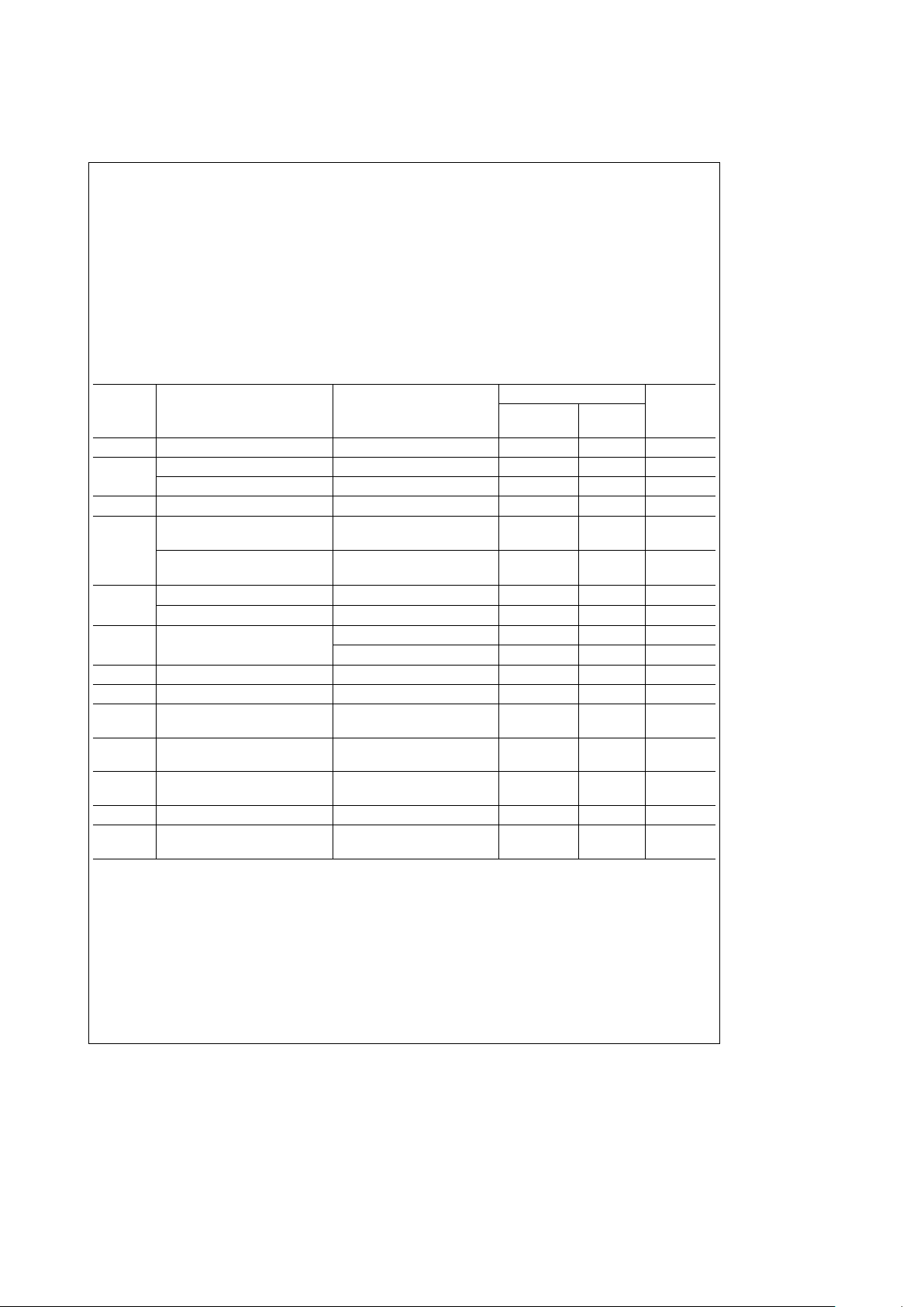
Electrical Characteristics
The following specifications apply for Vae8V, V
beb
5V, R
L
e
R
F
e
2kXand 0
§
s
T
J
s
60§C unless otherwise noted.
Symbol Parameter Conditions
LM6104M
Units
Typical Limits
(Note 4) (Note 5)
V
OS
Input Offset Voltage 10 30 mV max
I
B
Inverting Input Bias Current 5.0 20 mA max
Non-Inverting Input Bias Current 0.5 2 mA max
I
S
Supply Current V
O
e
0V 3.5 4.0 mA max
I
SC
Output Source Current V
O
e
0V
60 45
mA
I
IN(b)
eb
100 mA min
Output Sink Current V
O
e
0V
60 45
mA
I
IN(b)
e
100 mA min
V
O
Positive Output Swing I
IN(b)
eb
100 mA 6.5 6.1 V min
Negative Output Swing I
IN(b)
e
100 mA
b
3.5
b
3.1 V max
PSRR Power Supply Rejection Ratio V
S
e
g
4tog10V 70 60 dB min
100 mV pp@100 kHz 40 30 dB min
R
T
Transresistance 10 5 MX min
SR Slew Rate (Note 6) 100 55 V/ms min
BW Bandwidth A
V
eb
1
7.5 5.0 MHz
R
IN
e
R
F
e
2kX
Amp-to-Amp Isolation R
L
e
2kX
60 dB
F
e
1 MHz
CMVR Common Mode Voltage Range V
a
b
1.4V
V
V
b
a
1.4V
CMRR Common Mode Rejection Ratio 60 dB
t
S
Settling Time 0.05%, 5V Step, A
V
eb
1
240 ns
R
F
e
R
S
e
2kX,V
S
e
g
5V
Note 1: Absolute Maximum Ratings indicate limits beyond which damage to the device may occur. DC and AC electrical specifications do not apply when operating
the device beyond its rated operating conditions. Operating ratings indicate conditions the device is intended to be functional, but device parameter specifications
may not be guaranteed under the conditions.
Note 2: Human body model 1.5 kX and 100 pF. This is a class 2 device rating.
Note 3: Thermal resistance of the SO package is 98
§
C/W. When operating at T
A
e
80§C, maximum power dissipation is 700 mW.
Note 4: Typical values represent the most likely parametric norm.
Note 5: All limits guaranteed at operating temperature extremes.
Note 6: A
V
eb
1 with R
IN
e
R
F
e
2kX. Slew rate is calculated from the 25% to the 75% point on both rising and falling edges. Output swing isb0.6V toa5.6V
and 5.6V to 0.6V.
2
 Loading...