

LM566C Voltage Controlled Oscillator
Y
General Description
The LM566CN is a general purpose voltage controlled oscillator which may be used to generate square and triangular
waves, the frequency of which is a very linear function of a
control voltage. The frequency is also a function of an external resistor and capacitor.
The LM566CN is specified for operation over the 0
a
70§C temperature range.
Cto
§
Features
Y
Wide supply voltage range: 10V to 24V
Y
Very linear modulation characteristics
High temperature stability
Y
Excellent supply voltage rejection
Y
10 to 1 frequency range with fixed capacitor
Y
Frequency programmable by means of current, voltage,
resistor or capacitor
Applications
Y
FM modulation
Y
Signal generation
Y
Function generation
Y
Frequency shift keying
Y
Tone generation
LM566C Voltage Controlled Oscillator
February 1995
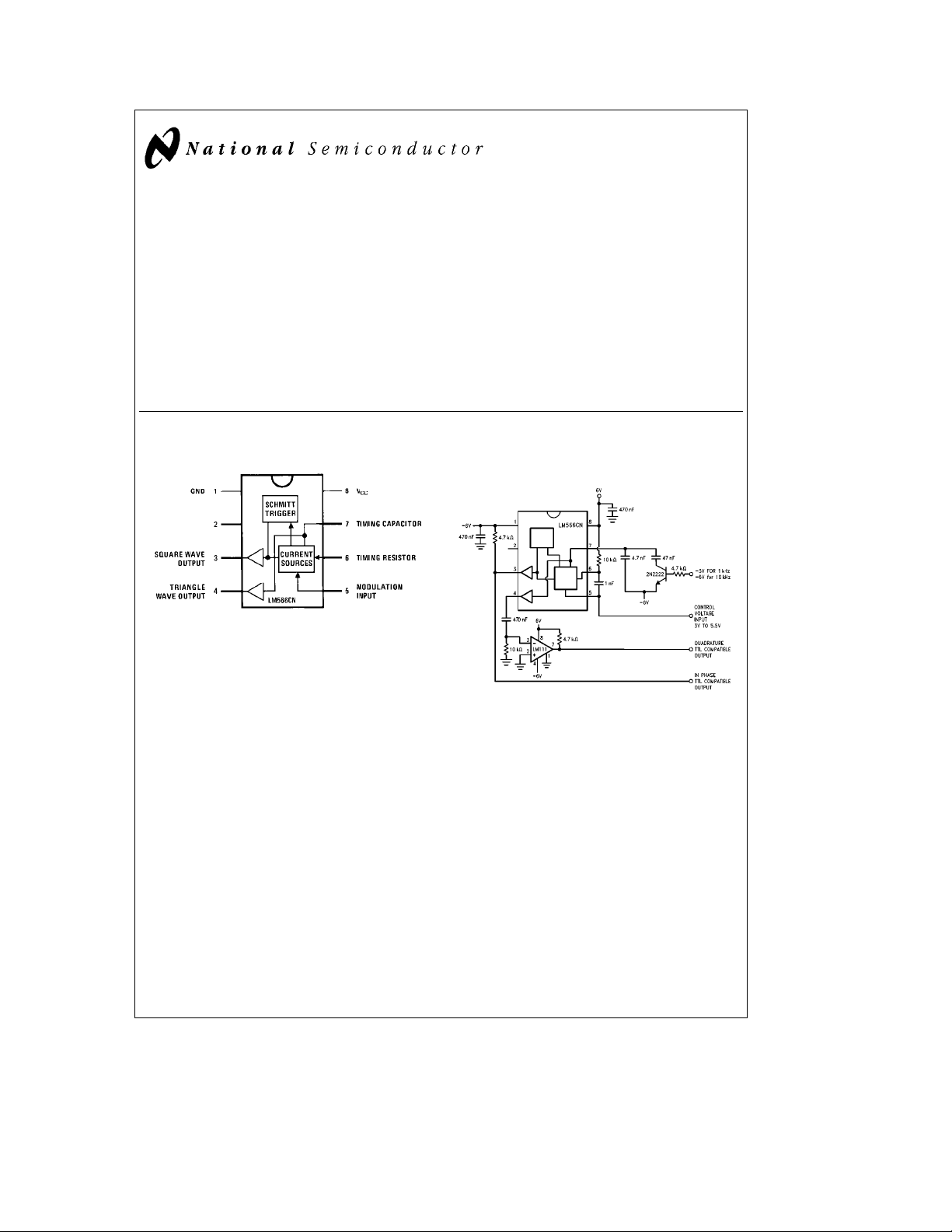
Connection Diagram
Dual-In-Line Package
Order Number LM566CN
See NS Package Number N08E
Typical Application
1 kHz and 10 kHz TTL Compatible
Voltage Controlled Oscillator
TL/H/7854– 2
TL/H/7854– 3
C
1995 National Semiconductor Corporation RRD-B30M115/Printed in U. S. A.
TL/H/7854
Absolute Maximum Ratings
If Military/Aerospace specified devices are required,
please contact the National Semiconductor Sales
Office/Distributors for availability and specifications.
Power Supply Voltage 26V
Power Dissipation (Note 1) 1000 mW
Operating Temperature Range, LM566CN 0
Lead Temperature (Soldering, 10 sec.)
Ctoa70§C
§
a
260§C
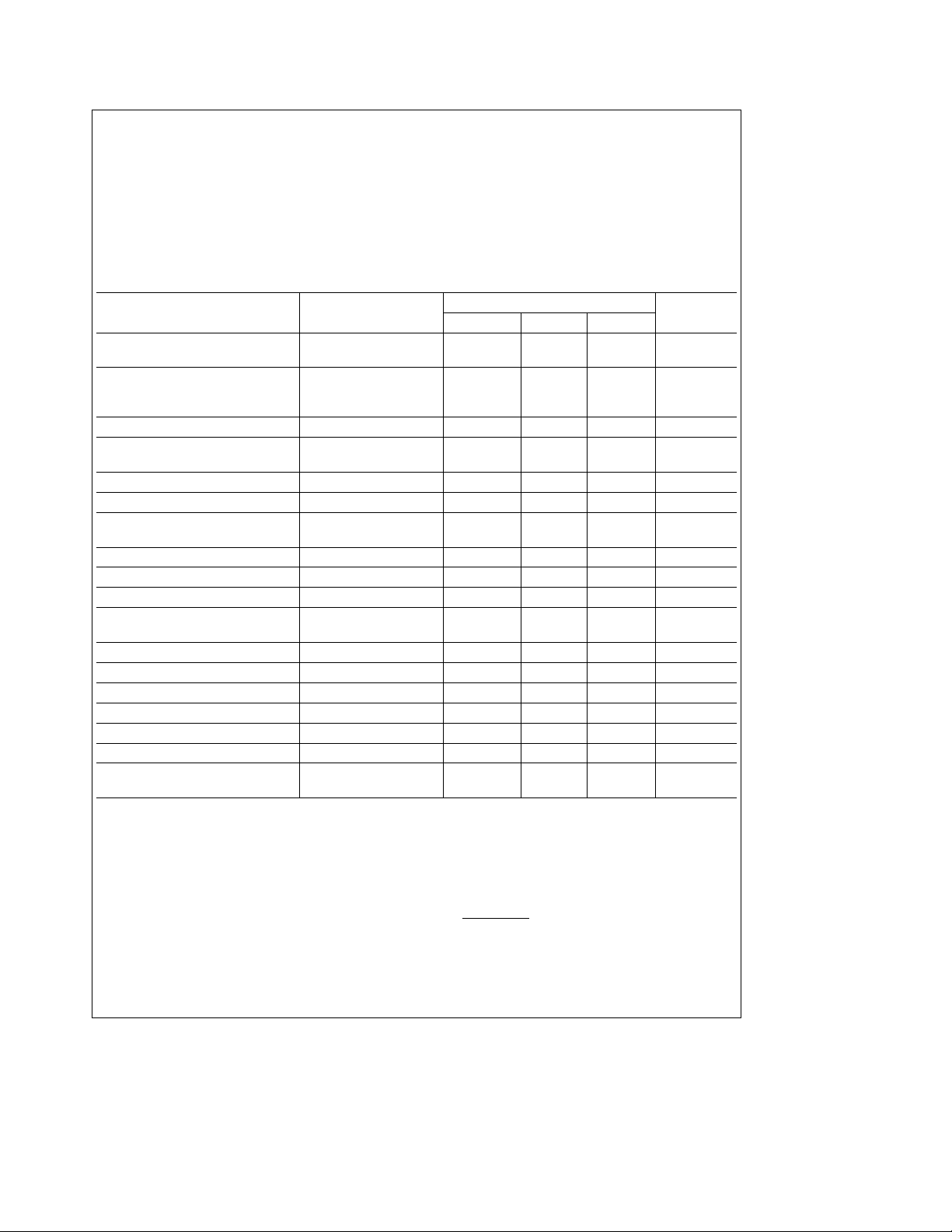
Electrical Characteristics V
Parameter Conditions
CC
e
12V, T
e
25§C, AC Test Circuit
A
LM566C
Units
Min Typ Max
Maximum Operating R0e2k
Frequency C0
VCO Free-Running C
Frequency R
e
2.7 pF
e
1.5 nF
O
e
20k
O
e
f
10 kHz
O
Input Voltage Range Pin 5 */4 V
Average Temperature Coefficient
of Operating Frequency
0.5 1 MHz
b
30 0
CC
a
30 %
V
CC
200 ppm/
C
§
Supply Voltage Rejection 10–20V 0.1 2 %/V
Input Impedance Pin 5 0.5 1 MX
VCO Sensitivity For Pin 5, From
e
O
10% Deviation 0.2 1.5 %
FM Distortion
8–10V, f
g
10 kHz
6.0 6.6 7.2 kHz/V
Maximum Sweep Rate 1 MHz
Sweep Range 10:1
Output Impedance
Pin 3 50 X
Pin 4 50 X
Square Wave Output Level R
Triangle Wave Output Level R
e
10k 5.0 5.4 Vp-p
L1
e
10k 2.0 2.4 Vp-p
L2
Square Wave Duty Cycle 40 50 60 %
Square Wave Rise Time 20 ns
Square Wave Fall Time 50 ns
Triangle Wave Linearity
Note 1: The maximum junction temperature of the LM566CN is 150§C. For operation at elevated junction temperatures, maximum power dissipation must be
derated based on a thermal resistance of 115
a
1V Segment at
(/2 V
CC
C/W, junction to ambient.
§
0.5 %
Applications Information
The LM566CN may be operated from either a single supply
as shown in this test circuit, or from a split (
ply. When operating from a split supply, the square wave
output (pin 3) is TTL compatible (2 mA current sink) with the
addition of a 4.7 kX resistor from pin 3 to ground.
g
) power sup-
A 0.001 mF capacitor is connected between pins 5 and 6 to
prevent parasitic oscillations that may occur during VCO
switching.
a
b
2.4(V
e
f
O
ROCOV
V5)
a
where
k
2KkR
and V
20K
O
is voltage between pin 5 and pin 1.
5
2
 Loading...