

LM565/LM565C
Phase Locked Loop
General Description
The LM565 and LM565C are general purpose phase locked
loops containing a stable,highly linear voltage controlled oscillator for low distortion FM demodulation, and a double balanced phase detector with good carrier suppression. The
VCO frequency is set with an external resistor and capacitor,
and a tuning range of 10:1 can be obtained with the same
capacitor. The characteristics of the closed loop
system—bandwidth, response speed, capture and pull in
range—may be adjusted over a wide range with an external
resistor and capacitor. The loop may be broken between the
VCO and the phase detector for insertion of a digital frequency divider to obtain frequency multiplication.
The LM565H is specified for operation over the −55˚C to
+125˚C military temperature range. The LM565CN is specified for operation over the 0˚C to +70˚C temperature range.
Features
n 200 ppm/˚C frequency stability of the VCO
n Power supply range of
±
5to±12 volts with 100 ppm/
%
typical
n 0.2%linearity of demodulated output
n Linear triangle wave with in phase zero crossings
available
n TTL and DTL compatible phase detector input and
square wave output
n Adjustable hold in range from
±
1%to
>
±
60
%
Applications
n Data and tape synchronization
n Modems
n FSK demodulation
n FM demodulation
n Frequency synthesizer
n Tone decoding
n Frequency multiplication and division
n SCA demodulators
n Telemetry receivers
n Signal regeneration
n Coherent demodulators
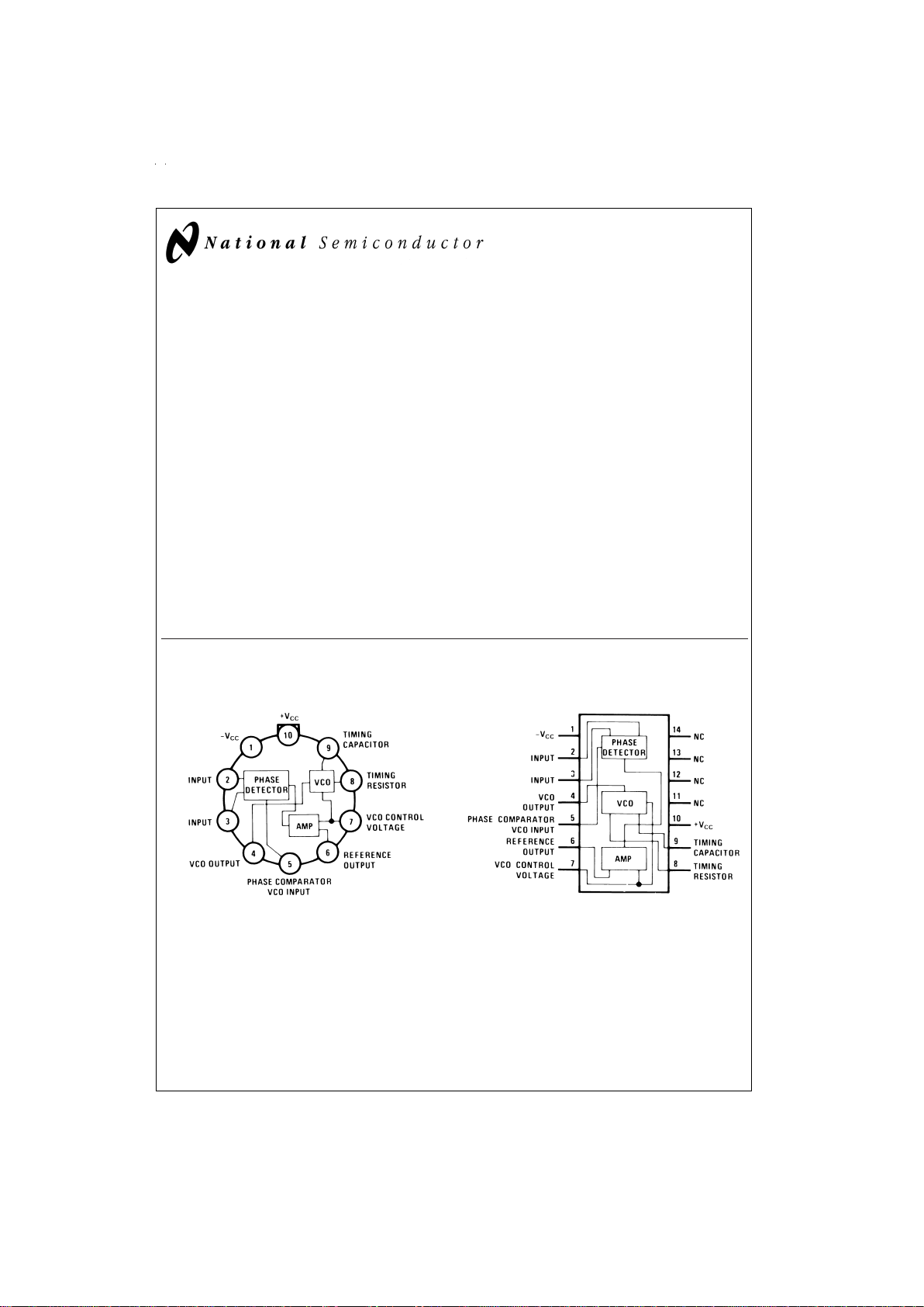
Connection Diagrams
Metal Can Package
DS007853-2
Order Number LM565H
See NS Package Number H10C
Dual-in-Line Package
DS007853-3
Order Number LM565CN
See NS Package Number N14A
May 1999
LM565/LM565C Phase Locked Loop
© 1999 National Semiconductor Corporation DS007853 www.national.com
Absolute Maximum Ratings (Note 1)
If Military/Aerospace specified devices are required,
please contact the National Semiconductor Sales Office/
Distributors for availability and specifications.
Supply Voltage
±
12V
Power Dissipation (Note 2) 1400 mW
Differential Input Voltage
±
1V
Operating Temperature Range
LM565H −55˚C to +125˚C
LM565CN 0˚C to +70˚C
Storage Temperature Range −65˚C to +150˚C
Lead Temperature
(Soldering, 10 sec.) 260˚C
Electrical Characteristics
AC Test Circuit, T
A
=
25˚C, V
CC
=
±
6V
Parameter Conditions
LM565 LM565C
Units
Min Typ Max Min Typ Max
Power Supply Current 8.0 12.5 8.0 12.5 mA
Input Impedance (Pins 2, 3) −4V
<
V2,V
3
<
0V 7 10 5 kΩ
VCO Maximum Operating
Frequency
C
o
=
2.7 pF
300 500 250 500 kHz
VCO Free-Running Frequency C
o
=
1.5 nF
R
o
=
20 kΩ
f
o
=
10 kHz
−10 0 +10 −30 0 +30
%
Operating Frequency
Temperature Coefficient
−100 −200 ppm/˚C
Frequency Drift with
Supply Voltage
0.1 1.0 0.2 1.5
%
/V
Triangle Wave Output Voltage 2 2.4 3 2 2.4 3 V
p-p
Triangle Wave Output Linearity 0.2 0.5
%
Square Wave Output Level 4.7 5.4 4.7 5.4 V
p-p
Output Impedance (Pin 4) 5 5 kΩ
Square Wave Duty Cycle 45 50 55 40 50 60
%
Square Wave Rise Time 20 20 ns
Square Wave Fall Time 50 50 ns
Output Current Sink (Pin 4) 0.6 1 0.6 1 mA
VCO Sensitivity f
o
=
10 kHz 6600 6600 Hz/V
Demodulated Output Voltage
(Pin 7)
±
10%Frequency Deviation
250 300 400 200 300 450 mV
p-p
Total Harmonic Distortion
±
10%Frequency Deviation 0.2 0.75 0.2 1.5
%
Output Impedance (Pin 7) 3.5 3.5 kΩ
DC Level (Pin 7) 4.25 4.5 4.75 4.0 4.5 5.0 V
Output Offset Voltage
|V
7−V6
|
30 100 50 200 mV
Temperature Drift of |V
7−V6
| 500 500 µV/˚C
AM Rejection 30 40 40 dB
Phase Detector Sensitivity K
D
0.68 0.68 V/radian
Note 1: Absolute Maximum Ratings indicate limits beyond which damage to the device may occur. Operating Ratings indicate conditions for which the device is functional, but do not guarantee specific performance limits. Electrical CharacteristicsstateDCandACelectricalspecificationsunderparticulartestconditionswhichguarantee specific performance limits. This assumes that the device is within the Operating Ratings. Specifications are not guaranteed for parameters where no limit is
given, however, the typical value is a good indication of device performance.
Note 2: The maximum junction temperature of the LM565 and LM565C is +150˚C. For operation at elevated temperatures, devices in the TO-5 package must be
derated based on a thermal resistance of +150˚C/W junction to ambient or +45˚C/W junction to case. Thermal resistance of the dual-in-line package is +85˚C/W.
www.national.com 2
Typical Performance Characteristics
Power Supply Current as a
Function of Supply Voltage
DS007853-14
Lock Range as a Function
of Input Voltage
DS007853-15
VCO Frequency
DS007853-16
Oscillator Output
Waveforms
DS007853-17
Phase Shift vs Frequency
DS007853-18
VCO Frequency as a
Function of Temperature
DS007853-19
Loop Gain vs Load
Resistance
DS007853-20
Hold in Range as a
Function of R
6–7
DS007853-21
www.national.com3
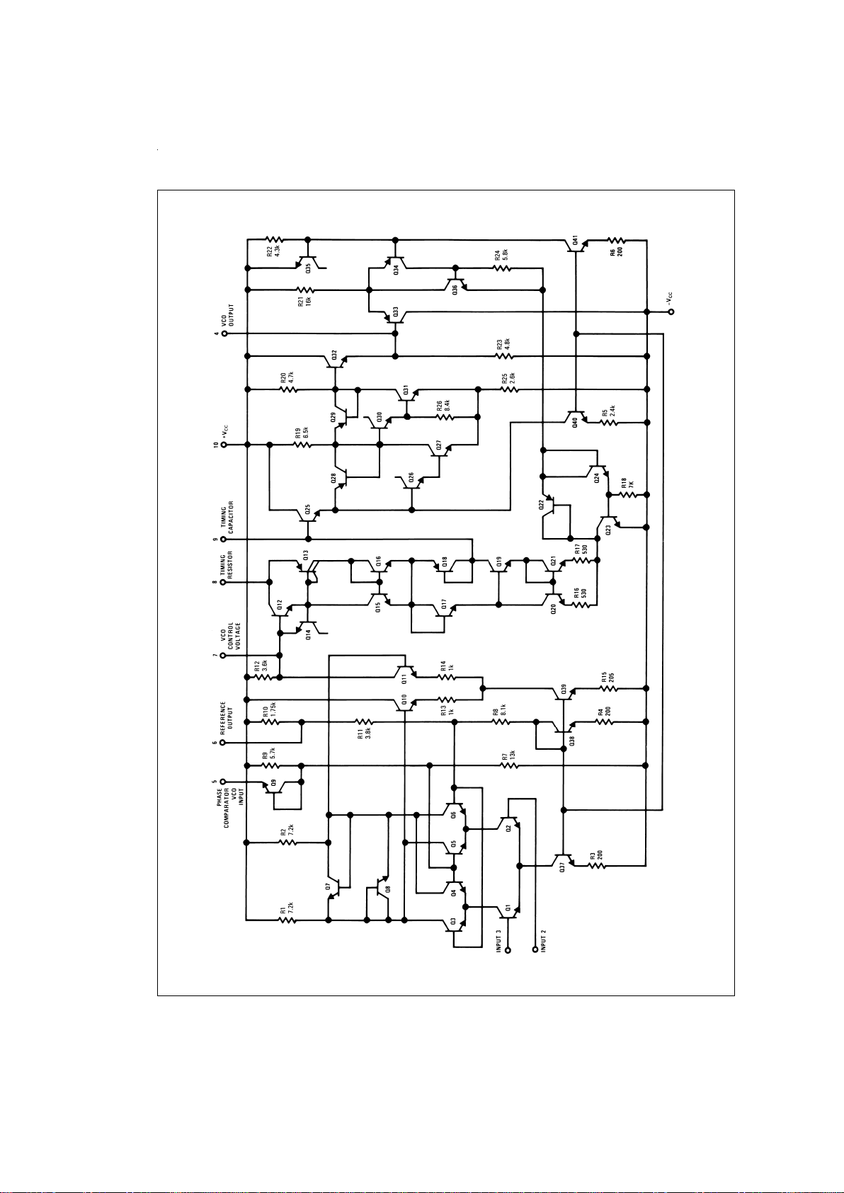
Schematic Diagram
DS007853-1
www.national.com 4
 Loading...