

LM5116 Evaluation Board
National Semiconductor
Application Note 1596
Robert Sheehan
May 2007
Introduction
The LM5116 evaluation board is designed to provide the design engineer with a fully functional power converter based
on Emulated Current Mode Control to evaluate the LM5116
controller IC. The evaluation board provides a 5V output with
a 7A current capability. The wide input voltage ranges from
7V to 60V. The design operates at 250kHz, a good compromise between conversion efficiency and solution size. The
printed circuit board consists of 4 layers, 2 ounce copper top
and bottom, 1 ounce copper internal layers on FR4 material
with a thickness of 0.06 inches. This application note contains
the evaluation board schematic, Bill-of-Materials (BOM) and
a quick setup procedure. Refer to the LM5116 datasheet for
complete circuit design information.
30012225
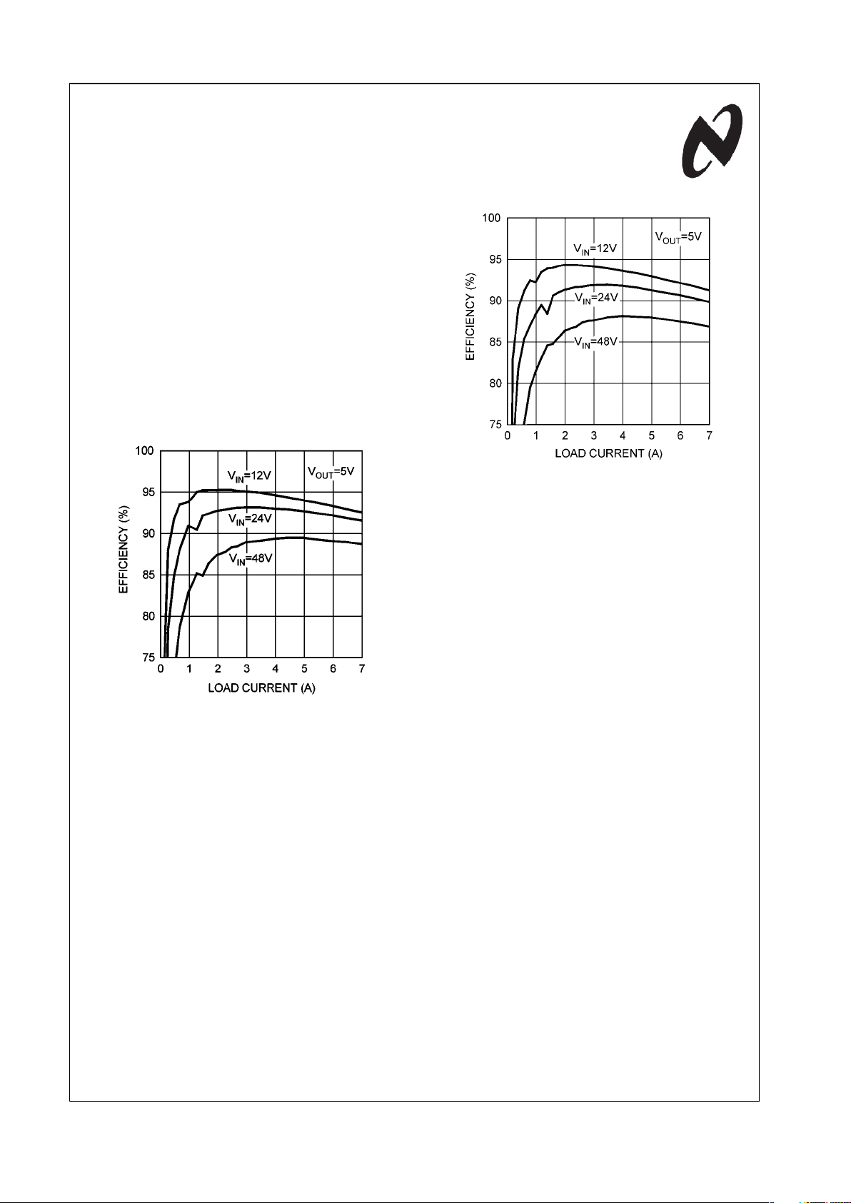
FIGURE 1. Efficiency with 6 µH Cooper Inductor
The performance of the evaluation board is as follows:
Input Range: 7V to 60V
Output Voltage: 5V
Output Current: 0 to 7A
Frequency of Operation: 250 kHz
Board Size: 2.55 X 2.65 X 0.5 inches
Load Regulation: 1%
Line Regulation: 0.1%
Over Current Limiting
30012223
FIGURE 2. Efficiency with 5.6 µH Pulse Inductor
Powering and Loading
Considerations
Read this entire page prior to attempting to power the evaluation board.
QUICK SETUP PROCEDURE
Step 1: Set the power supply current limit to 15A. Turn off the
power supply. Connect the power supply to the VIN terminals.
Step 2: Connect the load, with a 7A capability, to the V
OUT
terminals. Positive connection to P3 and negative connection
to P4.
Step 3: The EN pin should be left open for normal operation.
Step 4: Set VIN to 48V with no load applied. V
OUT
should be
in regulation with a nominal 5V output.
Step 5: Slowly increase the load while monitoring the output
voltage, V
OUT
should remain in regulation with a nominal 5V
output as the load is increased up to 7 Amps.
Step 6: Slowly sweep the input voltage from 7 to 60V, V
OUT
should remain in regulation with a nominal 5V output.
Step 7: Temporally short the EN pin to GND to check the
shutdown function.
Step 8: Increase the load beyond the normal range to check
current limiting. The output current should limit at approximately 11A. Cooling is critical during this step.
© 2007 National Semiconductor Corporation 300122 www.national.com
LM5116 Evaluation Board AN-1596
AIR FLOW
Prolonged operation with high input voltage at full power will
cause the MOSFETs to overheat. A fan with a minimum of
200 LFM should always be provided.
30012209
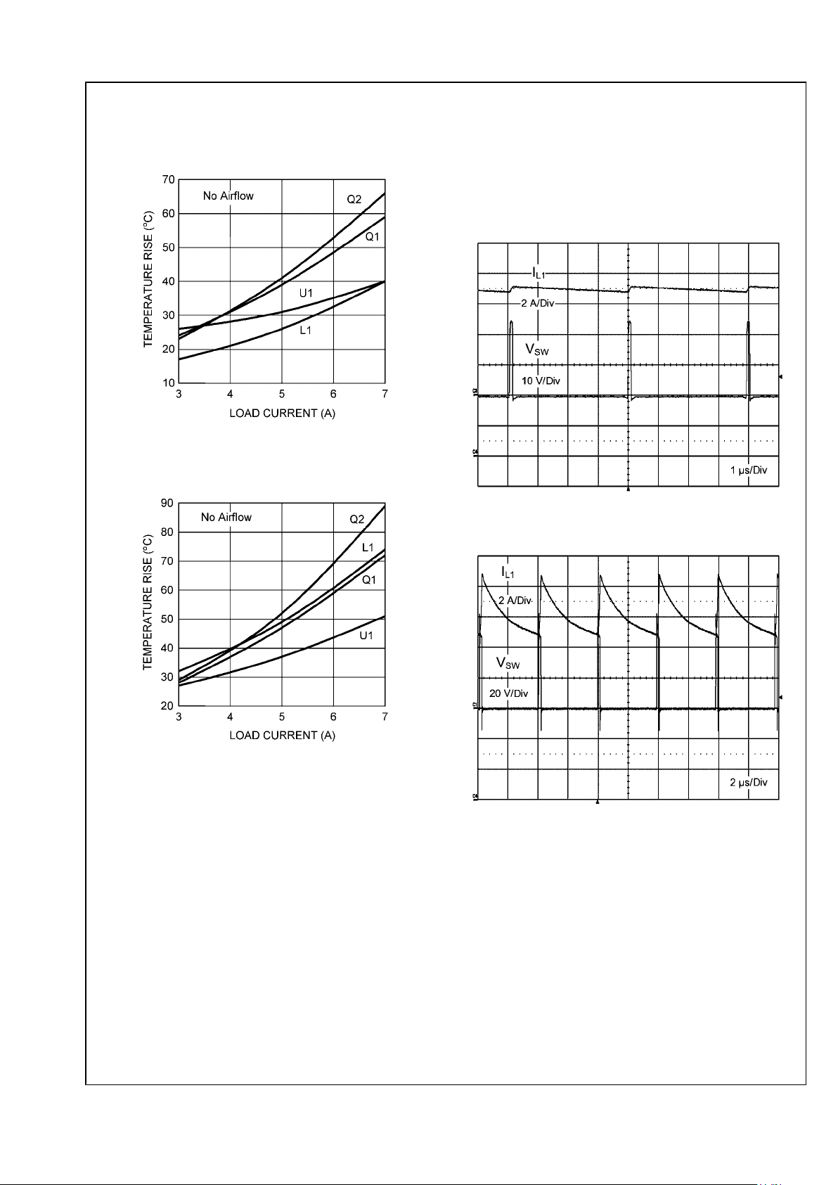
FIGURE 3. Temperature Rise at 48VIN with 6 µH Cooper
Inductor
30012222
FIGURE 4. Temperature Rise at 48VIN with 5.6 µH Pulse
Inductor
POWERING UP
Using the enable pin provided will allow powering up the
source supply with the current level set low. It is suggested
that the load be kept low during the first power up. Set the
current limit of the source supply to provide about 1.5 times
the anticipated wattage of the load. As you remove the connection from the enable pin to ground, immediately check for
5 volts at the output.
A quick efficiency check is the best way to confirm that everything is operating properly. If something is amiss you can
be reasonably sure that it will affect the efficiency adversely.
Few parameters can be incorrect in a switching power supply
without creating losses and potentially damaging heat.
For operation at 7VIN with full load, a 100 µF aluminum electrolytic capacitor installed across VIN will prevent input filter
oscillation for a typical bench test setup. See the LM5116 data
sheet for complete design information.
OVER CURRENT PROTECTION
The evaluation board is configured with over-current protection. The output current is limited to approximately 11A. The
thermal stress is quite severe while in an overloaded condition. Limit the duration of the overload and provide sufficient
cooling (airflow).
30012202
FIGURE 5. Short Circuit at 24VIN Room Temperature
30012203
FIGURE 6. Short Circuit at 48VIN 125°C
For sustained short circuit protection, adding C7 ≥ 1 µF will
limit the short circuit power dissipation. D2 should be installed
when using C7.
www.national.com 2
AN-1596
30012204
FIGURE 7. Short Circuit Recovery into Resistive Load
with C7 = 1 µF and D2 Installed
VCCX
This test point supports evaluation of an auxiliary supply voltage derived from V
OUT
. For output voltages between 7V and
14V, a zero ohm resistor may be installed for R12. The selected MOSFETs need greater than 6V gate drive to fully
enhance them for lowest R
DS(ON)
, so R12 is not recommended
for the 5V output.
Under no circumstances should an external voltage source
be connected to VCCX when VIN < VCC. Damage to the controller will result. A series diode from the input voltage source
to pin 1 is required to accommodate VIN < VCC.
SYNCHRONIZATION
A SYNC pin has been provided on the evaluation board. This
pin can be used to synchronize the regulator to an external
clock. Refer to the LM5116 datasheet for complete information.
30012207
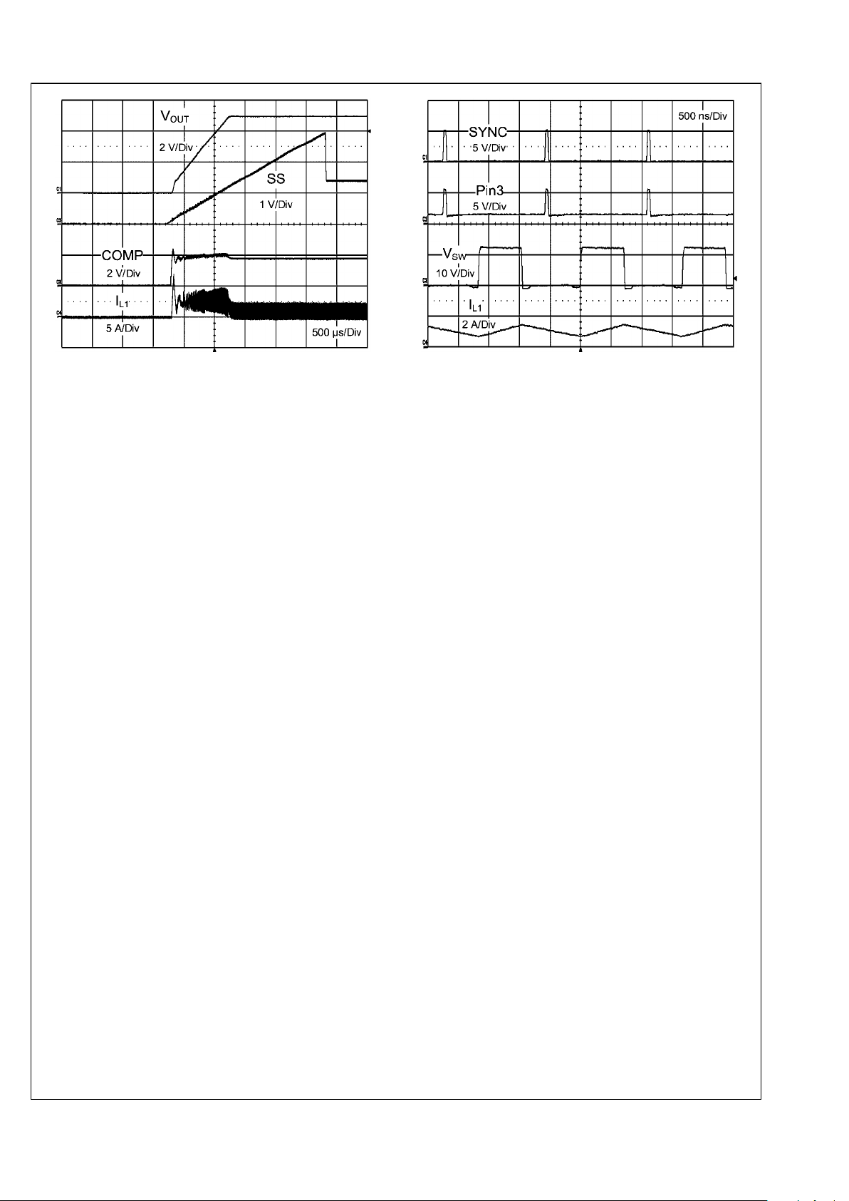
FIGURE 8. Synchronization at 12V
IN
ACTIVE LOADS
Figure 12 shows a typical start-up characteristic into a constant current active load. This type of load can exhibit an initial
short circuit, which is sustained well beyond the normal softstart cycle. Overshoot of the output voltage is possible with
this condition. Increasing the soft-start time to be longer than
the initial short circuit period of the active load will minimize
any possible overshoot. When using C7, the hiccup off-time
may also need adjustment.
3 www.national.com
AN-1596
Typical Performance Waveforms
30012206
FIGURE 9. Full Synchronous Operation at 48VIN with
JMP1 Removed
30012201
FIGURE 10. Discontinuous Operation using Diode
Emulation Mode at 60VIN with JMP1 Installed
30012208
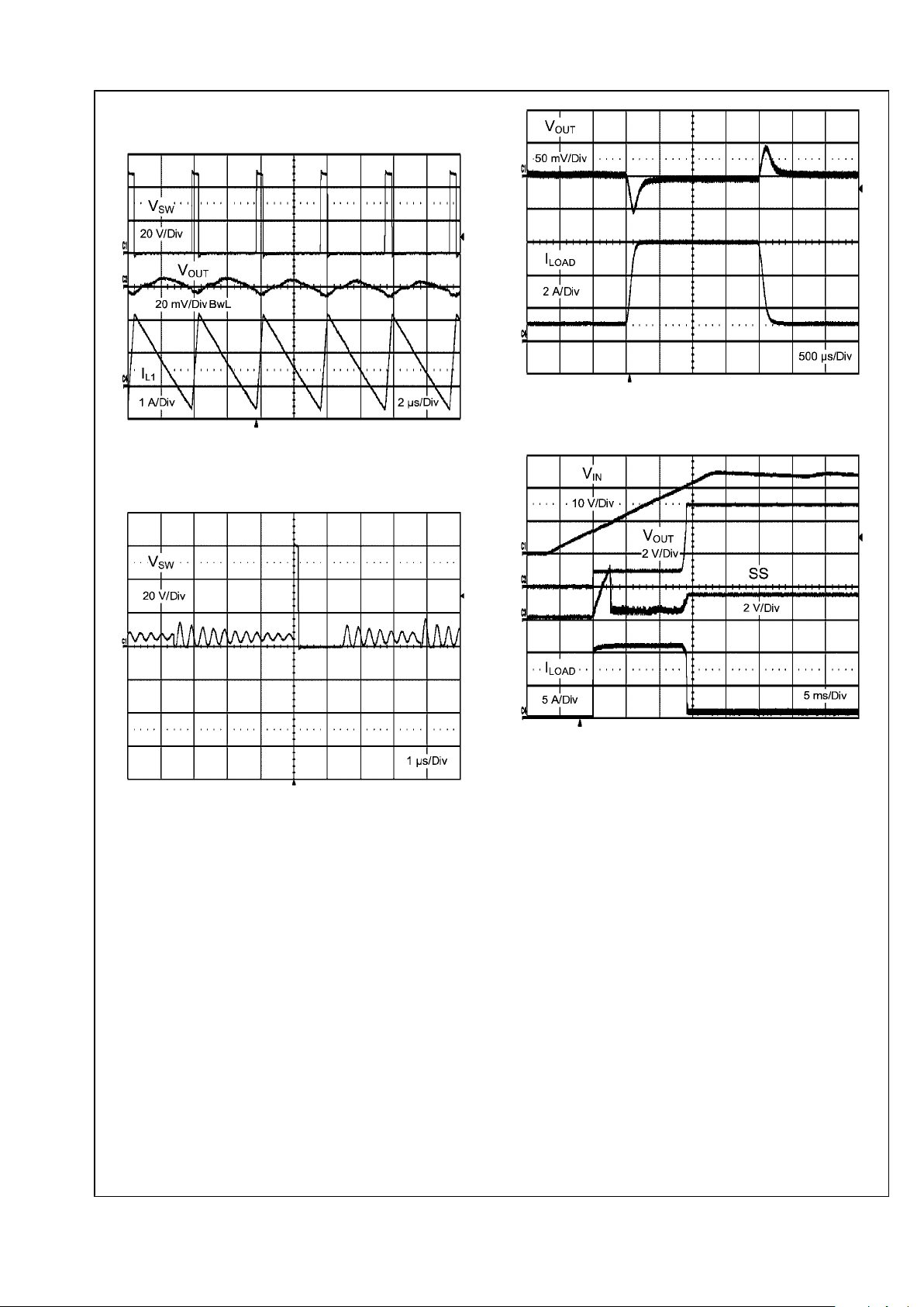
FIGURE 11. Transient Response at 24V
IN
30012205
FIGURE 12. Start-up into Active Load at 24V
IN
www.national.com 4
AN-1596
 Loading...