NSC LM5116 Datasheet
April 2007
LM5116
Wide Range Synchronous Buck Controller
General Description
The LM5116 is a synchronous buck controller intended for
step-down regulator applications from a high voltage or widely
varying input supply. The control method is based upon current mode control utilizing an emulated current ramp. Current
mode control provides inherent line feed-forward, cycle by
cycle current limiting and ease of loop compensation. The use
of an emulated control ramp reduces noise sensitivity of the
pulse-width modulation circuit, allowing reliable control of
very small duty cycles necessary in high input voltage applications. The operating frequency is programmable from
50kHz to 1MHz. The LM5116 drives external high-side and
low-side NMOS power switches with adaptive dead-time control. A user-selectable diode emulation mode enables discontinuous mode operation for improved efficiency at light load
conditions. A low quiescent current shutdown disables the
controller and consumes less than 10µA of total input current.
Additional features include a high voltage bias regulator, automatic switch-over to external bias for improved efficiency,
thermal shutdown, frequency synchronization, cycle by cycle
current limit and adjustable line under-voltage lockout. The
device is available in a power enhanced TSSOP-20 package
featuring an exposed die attach pad to aid thermal dissipation.
Features
■
Emulated peak current mode
■
Wide operating range up to 100V
■
Low IQ shutdown (<10µA)
■
Drives standard or logic level MOSFETs
■
Robust 3.5A peak gate drive
■
Free-run or synchronous operation to 1MHz
■
Optional diode emulation mode
■
Programmable output from 1.215V to 80V
■
Precision 1.5% voltage reference
■
Programmable current limit
■
Programmable soft-start
■
Programmable line under-voltage lockout
■
Automatic switch to external bias supply
■
TSSOP-20EP exposed pad
■
Thermal shutdown
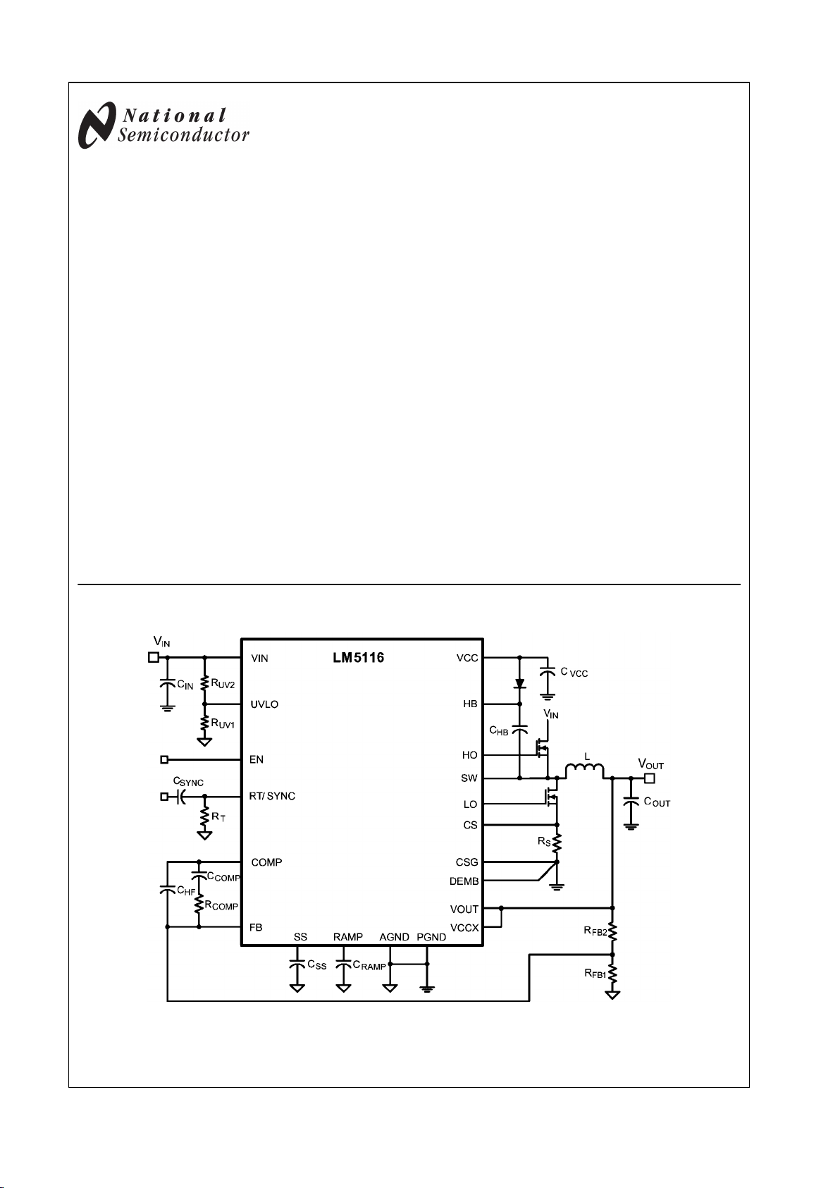
Typical Application
30007501
© 2007 National Semiconductor Corporation 300075 www.national.com
LM5116 Wide Range Synchronous Buck Controller
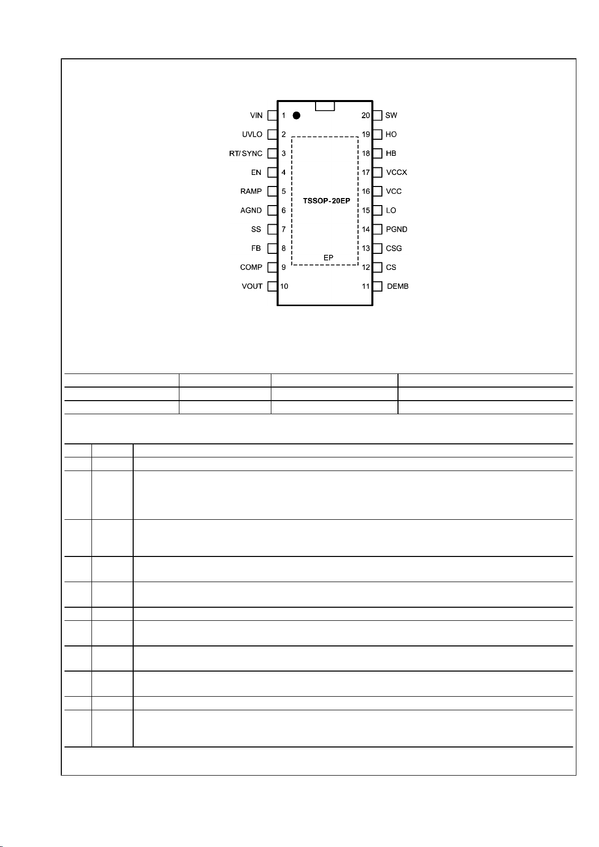
Connection Diagram
30007502
Top View
See NS Package Numbers MXA20A
Ordering Information
Ordering Number Package Type NSC Package Drawing Supplied As
LM5116MH TSSOP-20EP MXA20A 73 Units Per Anti-Static Tube
LM5116MHX TSSOP-20EP MXA20A 2500 units shipped as Tape & Reel
Pin Descriptions
Pin Name Description
1 VIN Chip supply voltage, input voltage monitor and input to the VCC regulator.
2 UVLO If the UVLO pin is below 1.215V, the regulator will be in standby mode (VCC regulator running, switching regulator
disabled). If the UVLO pin voltage is above 1.215V, the regulator is operational. An external voltage divider can be
used to set an under-voltage shutdown threshold. There is a fixed 5µA pull up current on this pin when EN is high.
UVLO is pulled to ground in the event a current limit condition exists for 256 clock cycles.
3 RT/
SYNC
The internal oscillator is set with a single resistor between this pin and the AGND pin. The recommended frequency
range is 50kHz to 1MHz. The internal oscillator can be synchronized to an external clock by AC coupling a positive
edge onto this node.
4 EN If the EN pin is below 0.5V, the regulator will be in a low power state drawing less than 10µA from VIN. EN must be
pulled above 3.3V for normal operation.
5 RAMP Ramp control signal. An external capacitor connected between this pin and the AGND pin sets the ramp slope used
for current mode control.
6 AGND Analog ground.
7 SS An external capacitor and an internal 10µA current source set the soft start time constant for the rise of the error amp
reference. The SS pin is held low during VCC < 4.5V, UVLO < 1.215V, EN input low or thermal shutdown.
8 FB Feedback signal from the regulated output. This pin is connected to the inverting input of the internal error amplifier.
The regulation threshold is 1.215V.
9 COMP Output of the internal error amplifier. The loop compensation network should be connected between this pin and the
FB pin.
10 VOUT Output monitor. Connect directly to the output voltage.
11 DEMB Low-side MOSFET source voltage monitor for diode emulation. For start-up into a pre-biased load, tie this pin to
ground at the CSG connection. For fully synchronous operation, use an external series resistor between DEMB and
ground to raise the diode emulation threshold above the low-side SW on-voltage.
www.national.com 2
LM5116
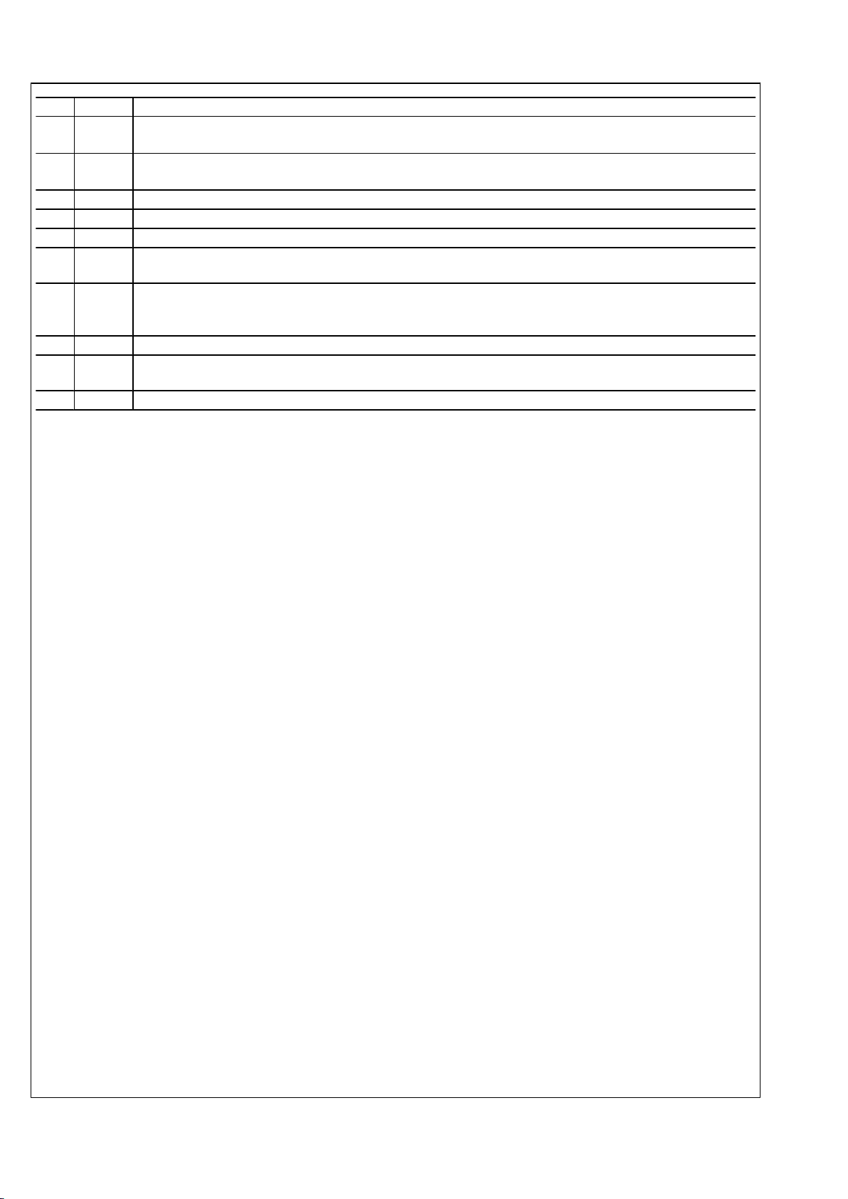
Pin Name Description
12 CS Current sense amplifier input. Connect to the top of the current sense resistor or the drain of the low-sided MOSFET
if R
DS(ON)
current sensing is used.
13 CSG Current sense amplifier input. Connect to the bottom of the sense resistor or the source of the low-side MOSFET if
R
DS(ON)
current sensing is used.
14 PGND Power ground.
15 LO Connect to the gate of the low-side synchronous MOSFET through a short, low inductance path.
16 VCC Locally decouple to PGND using a low ESR/ESL capacitor located as close to the controller as possible.
17 VCCX Optional input for an externally supplied VCC. If VCCX > 4.5V, VCCX is internally connected to VCC and the internal
VCC regulator is disabled. If VCCX is unused, it should be connected to ground.
18 HB High-side driver supply for bootstrap gate drive. Connect to the cathode of the bootstrap diode and the positive
terminal of the bootstrap capacitor. The bootstrap capacitor supplies current to charge the high-side MOSFET gate
and should be placed as close to the controller as possible.
19 HO Connect to the gate of the high-side synchronous MOSFET through a short, low inductance path
20 SW Switch node. Connect to the negative terminal of the bootstrap capacitor and the source terminal of the high-side
MOSFET.
EP EP Exposed pad. Solder to ground plane.
3 www.national.com
LM5116
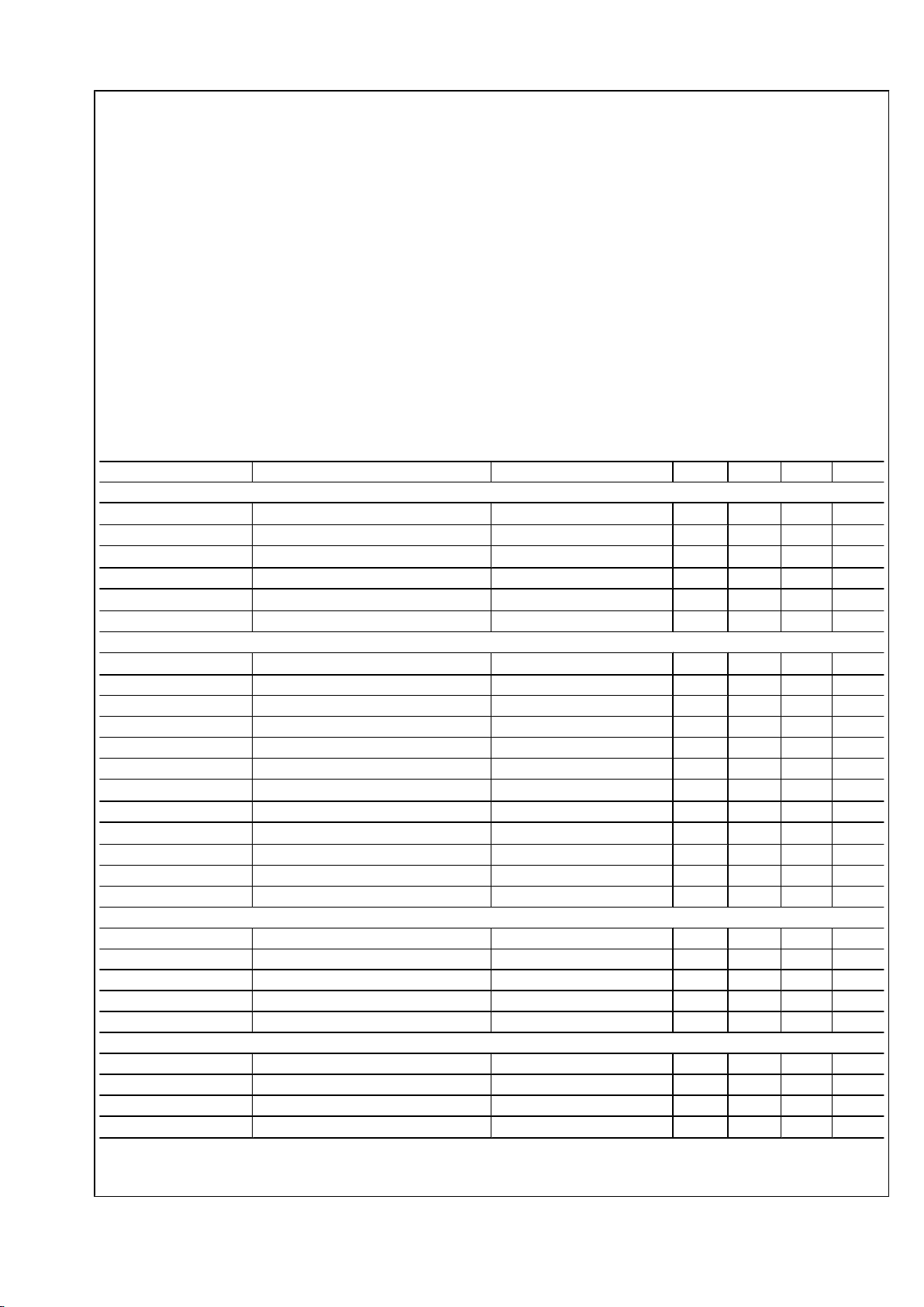
Absolute Maximum Ratings (Note 1)
If Military/Aerospace specified devices are required,
please contact the National Semiconductor Sales Office/
Distributors for availability and specifications.
VIN to GND -0.3V to 100V
VCC, VCCX, UVLO to GND (Note 3) -0.3 to 16V
SW, CS to GND -3.0 to 100V
HB to SW -0.3 to 16V
HO to SW -0.3 to HB+0.3V
VOUT to GND -0.3 to 100V
CSG to GND -1V to 1V
LO to GND -0.3 to VCC+0.3V
SS to GND -0.3 to 7V
FB to GND -0.3 to 7V
DEMB to GND -0.3 to VCC
RT to GND -0.3 to 7V
EN to GND -0.3 to 100V
ESD Rating
HBM (Note 2) 2 kV
Storage Temperature Range -55°C to +150°C
Junction Temperature +150°C
Operating Ratings (Note 1)
VIN 6V to 100V
VCC, VCCX 4.75V to 15V
HB to SW 4.75V to 15V
DEMB to GND -0.3V to 2V
Junction Temperature -40°C to +125°C
Note: RAMP, COMP are output pins. As such they are not specified to have
an external voltage applied.
Electrical Characteristics Limits in standard type are for T
J
= 25°C only; limits in boldface type apply over the
junction temperature range of -40°C to +125°C and are provided for reference only. Unless otherwise specified, the following
conditions apply: VIN = 48V, VCC = 7.4V, VCCX = 0V, EN = 5V, RT = 16kΩ, no load on LO and HO.
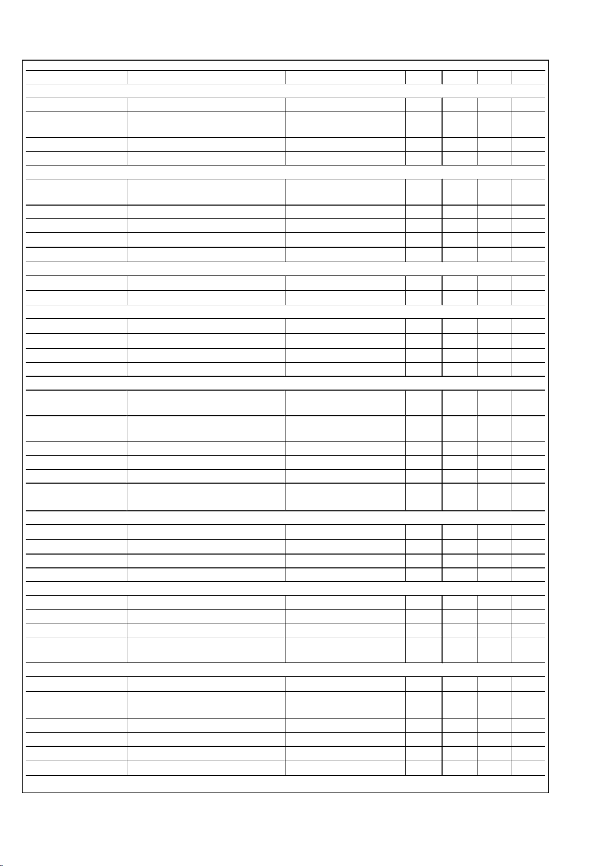
Symbol Parameter Conditions Min Typ Max Units
VIN Supply
I
BIAS
VIN Operating Current VCCX = 0V, VIN = 48V 5 7 mA
VCCX = 0V, VIN = 100V 5.9 8 mA
I
BIASX
VIN Operating Current VCCX = 5V, VIN = 48V 1.2 1.7 mA
VCCX = 5V, VIN = 100V 1.6 2.3 mA
I
STDBY
VIN Shutdown Current EN = 0V, VIN = 48V 1 10 µA
EN = 0V, VIN = 100V 1 µA
VCC Regulator
V
CC(REG)
VCC Regulation 7.1 7.4 7.7 V
VCC LDO Mode Turn-off 10.6 V
VCC Regulation VIN = 6V 5.0 5.9 6.0 V
VCC Sourcing Current Limit VCC = 0V 15 26 mA
VCCX Switch Threshold VCCX Rising 4.3 4.5 4.7 V
VCCX Switch Hysteresis 0.25 V
VCCX Switch R
DS(ON)
ICCX = 10mA 3.8 6.2
Ω
VCCX Leakage VCCX = 0V -200 nA
VCCX Pull- down Resistance VCCX = 3V 100
kΩ
VCC Under-voltage Threshold VCC Rising 4.3 4.5 4.7 V
VCC Under-voltage Hysteresis 0.2 V
HB DC Bias Current HB-SW = 15V 125 200 µA
EN Input
VIL max EN Input Low Threshold 0.5 V
VIH min EN Input High Threshold 3.3 V
EN Input Bias Current VEN = 3V -7.5 -3 1 µA
EN Input Bias Current VEN = 0.5V -1 0 1 µA
EN Input Bias Current VEN = 100V 20 90 µA
UVLO Thresholds
UVLO Standby Threshold UVLO Rising 1.170 1.215 1.262 V
UVLO Threshold Hysteresis 0.1 V
UVLO Pull-up Current Source UVLO = 0V 5.4 µA
UVLO Pull-down R
DS(ON)
80 210
Ω
www.national.com 4
LM5116
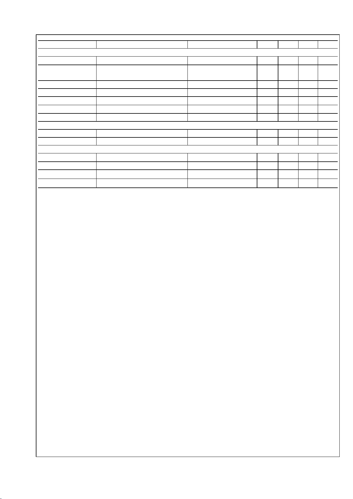
Symbol Parameter Conditions Min Typ Max Units
Soft Start
SS Current Source SS = 0V 8 11 14 µA
SS Diode Emulation Ramp Disable
Threshold
SS Rising 3 V
SS to FB Offset FB = 1.25V 160 mV
SS Output Low Voltage Sinking 100µA, UVLO = 0V 45 mV
Error Amplifier
V
REF
FB Reference Voltage Measured at FB pin, FB =
COMP
1.195 1.215 1.231 V
FB Input Bias Current FB = 2V 15 500 nA
COMP Sink/Source Current 3 mA
A
OL
DC Gain 80 dB
f
BW
Unity Gain Bandwidth 3 MHz
PWM Comparators
t
HO(OFF)
Forced HO Off-time 320 450 580 ns
t
ON(min)
Minimum HO On-time VIN = 80V, C
RAMP
= 50pF 100 ns
Oscillator
f
SW1
Frequency 1
RT = 16kΩ
180 200 220 kHz
f
SW2
Frequency 2
RT = 5kΩ
480 535 590 kHz
RT output voltage 1.191 1.215 1.239 V
RT sync positive threshold 3.0 3.5 4.0 V
Current Limit
V
CS(TH)
Cycle-by-cycle Sense Voltage
Threshold (CSG-CS)
VCCX = 0V, RAMP = 0V 94 110 126 mV
V
CS(THX)
Cycle-by-cycle Sense Voltage
Threshold (CSG-CS)
VCCX = 5V, RAMP = 0V 105 122 139 mV
CS Bias Current CS = 100V -1 1 µA
CS Bias Current CS = 0V 90 125 µA
CSG Bias Current CSG = 0V 90 125 µA
Current Limit Fault Timer
RT = 16kΩ, (200kHz), (256
clock cycles)
1.28 ms
RAMP Generator
I
R1
RAMP Current 1 VIN = 60V, VOUT=10V 235 285 335 µA
I
R2
RAMP Current 2 VIN = 10V, VOUT = 10V 21 28 35 µA
VOUT Bias Current VOUT = 36V 200 µA
RAMP Output Low Voltage VIN = 60V, VOUT = 10V 265 mV
Diode Emulation
SW Zero Cross Threshold -6 mV
DEMB Output Current DEMB = 0V, SS = 1.25V 1.6 2.7 3.8 µA
DEMB Output Current DEMB =0V, SS = 2.8V 28 38 48 µA
DEMB Output Current DEMB = 0V, SS = Regulated
by FB
45 65 85 µA
LO Gate Driver
V
OLL
LO Low-state Output Voltage ILO = 100mA 0.08 0.17 V
V
OHL
LO High-state Output Voltage ILO = -100mA, V
OHL
= VCC -
V
LO
0.25 V
LO Rise Time C-load = 1000pF 18 ns
LO Fall Time C-load = 1000pF 12 ns
I
OHL
Peak LO Source Current VLO = 0V 1.8 A
I
OLL
Peak LO Sink Current VLO = VCC 3.5 A
5 www.national.com
LM5116
Symbol Parameter Conditions Min Typ Max Units
HO Gate Driver
V
OLH
HO Low-state Output Voltage IHO = 100mA 0.17 0.27 V
V
OHH
HO High-state Output Voltage IHO = -100mA, V
OHH
= VHB –
V
HO
0.45 V
HO Rise Time C-load = 1000pF 19 ns
HO High-side Fall Time C-load = 1000pF 13 ns
I
OHH
Peak HO Source Current VHO = 0V 1 A
I
OLH
Peak HO Sink Current VHO = VCC 2.2 A
HB to SW under-voltage 3 V
Switching Characteristics
LO Fall to HO Rise Delay C-load = 0 75 ns
HO Fall to LO Rise Delay C-load = 0 70 ns
Thermal
T
SD
Thermal Shutdown Rising 170 °C
Thermal Shutdown Hysteresis 15 °C
θ
JA
Junction to Ambient 40 °C/W
θ
JC
Junction to Case 4 °C/W
Note 1: Absolute Maximum Ratings indicate limits beyond which damage to the component may occur. Operating Ratings are conditions under which operation
of the device is guaranteed. Operating Ratings do not imply guaranteed performance limits. For guaranteed performance limits and associated test conditions,
see the Electrical Characteristics tables.
Note 2: The human body model is a 100pF capacitor discharged through a 1.5kΩ resistor into each pin. LO, HO and HB are rated at 1kV. 2kV rating for all pins
except VIN which is rated for 1.5kV.
Note 3: These pins must not exceed VIN.
www.national.com 6
LM5116
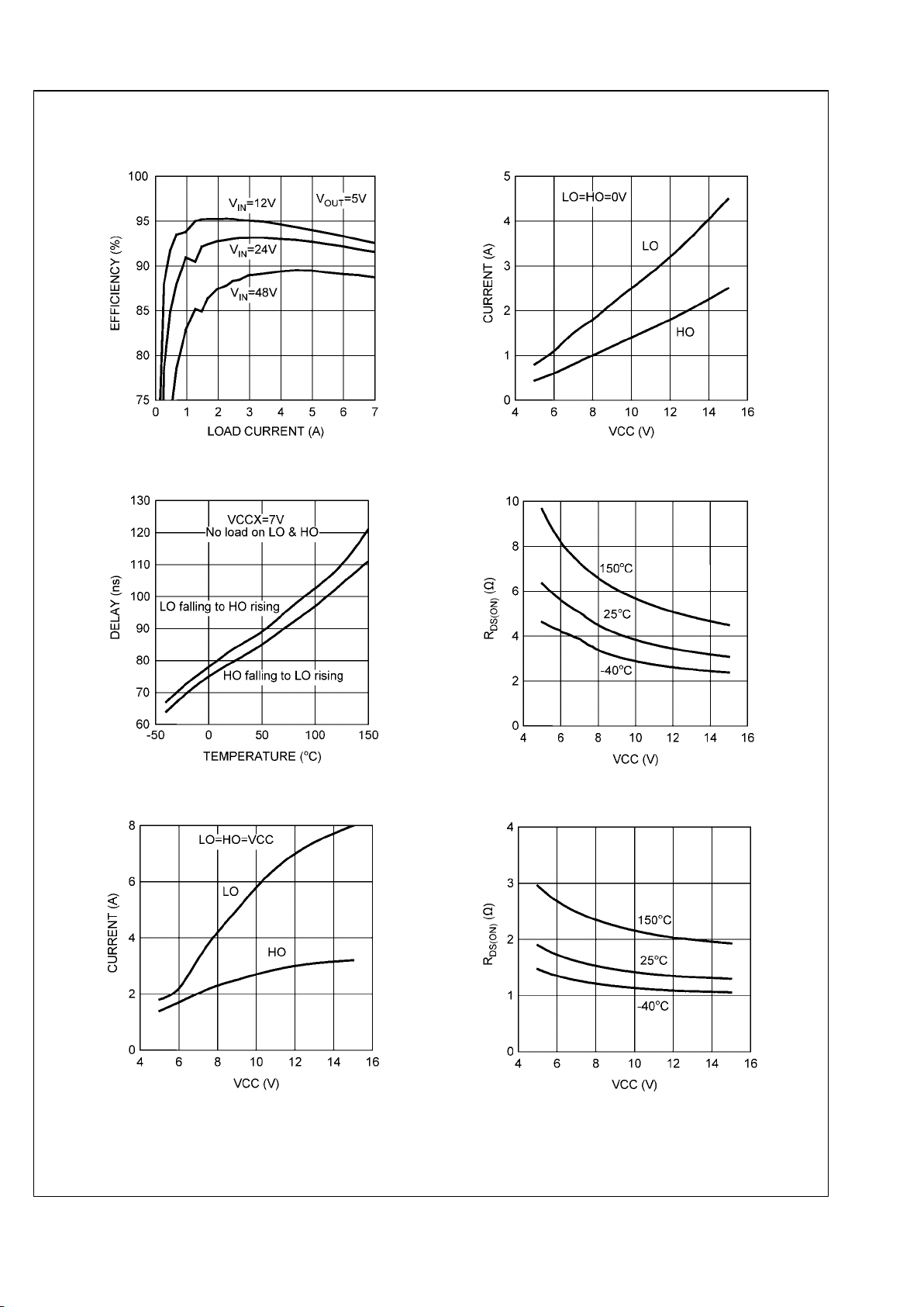
Typical Performance Characteristics
Typical Application Circuit Efficiency
30007503
Driver Source Current vs VCC
30007504
Driver Dead-time vs Temperature
30007505
HO High R
DS(ON)
vs VCC
30007506
Driver Sink Current vs VCC
30007507
HO Low R
DS(ON)
vs VCC
30007508
7 www.national.com
LM5116
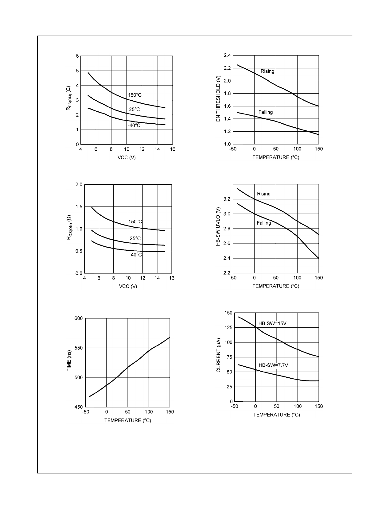
LO High R
DS(ON)
vs VCC
30007509
EN Input Threshold vs Temperature
30007510
LO Low R
DS(ON)
vs VCC
30007511
HB to SW UVLO vs Temperature
30007512
Forced HO Off-time vs Temperature
VCCX = 5V
30007513
HB DC Bias Current vs Temperature
30007514
www.national.com 8
LM5116
 Loading...