

NSC LM5073MH, LM5073 Datasheet
March 2007
LM5073
100V Power Over Ethernet PD Interface with Aux Support
General Description
The LM5073 Powered Device (PD) interface provides a high
performance solution that is fully compliant to IEEE 802.3af
for a PD connecting into Power over Ethernet (PoE) networks.
The LM5073 provides the flexibility for the PD to also accept
power from unregulated auxiliary sources such as AC
adapters and solar cells in a variety of configurations. The low
R
DS(ON)
PD interface hot swap MOSFET and programmable
DC current limit extend the range of LM5073 applications up
to twice the power level of IEEE 802.3af compliant devices.
The 100V maximum voltage rating simplifies selection of the
transient voltage suppressor that protects the PD from network transients. Control outputs for a separate DC-DC converter are provided to allow freedom to select the best DC-DC
converter topology for the particular application.
Features
PD Interface
■
Fully Compliant IEEE 802.3af PD Interface
■
Versatile Auxiliary Power Options
■
13V Minimum Front Auxiliary Power Range
■
9V Minimum Rear Auxiliary Power Range
■
Programmable DC Current Limit up to 800 mA
■
100V, 0.7Ω Hot Swap MOSFET
■
Integrated PD Signature Resistor
■
Integrated PoE Input UVLO
■
Inrush Current Limit
■
PD Classification Capability
■
Thermal Shutdown Protection
■
Line Over Voltage Protection
■
Complementary Open Drain Outputs for Controlling a DCDC Converter
■
Power Good Indicator
Applications
■
IEEE 802.3af Compliant PoE Powered Devices
■
Non-Compliant, Application Specific Devices
■
Higher Power Ethernet Powered Devices
Packages
■
TSSOP-14 EP (Exposed Pad)
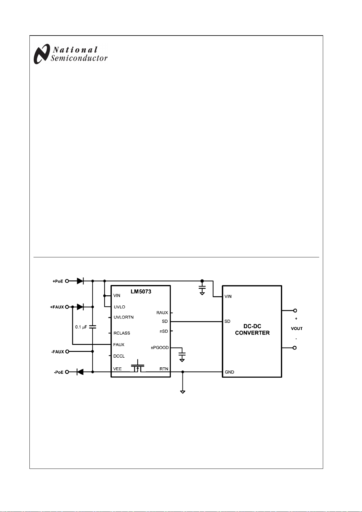
Simplified Application Diagram
30000201
© 2007 National Semiconductor Corporation 300002 www.national.com
LM5073 100V Power Over Ethernet PD Interface with Aux Support
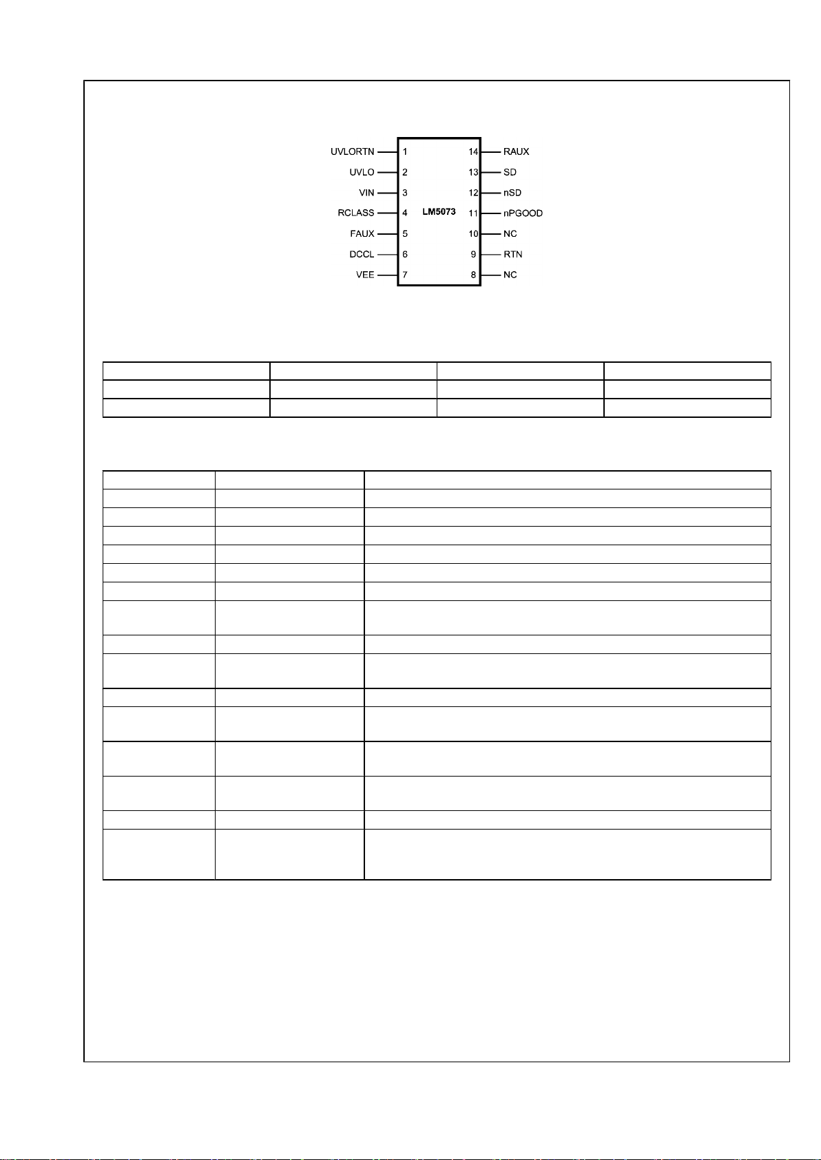
Connection Diagram
30000202
14 Lead TSSOP-EP
Ordering Information
Order Number Package Type NSC Package Drawing Supplied As
LM5073MH TSSOP-14EP MXA14A 94 Units per Rail
LM5073MHX TSSOP-14EP MXA14A 2500 Units on Tape and Reel
Pin Descriptions
Pin Number Name Description
1 UVLORTN Return for the external UVLO programming resistor divider.
2 UVLO Line under-voltage lockout programming pin.
3 VIN Positive supply pin for the PD interface and the DC-DC converter interface.
4 RCLASS PD Classification programming pin.
5 FAUX Front auxiliary power enable pin.
6 DCCL PD interface DC current limit programming pin.
7 VEE Negative supply pin for the PD interface; connected to PoE and/or front
auxiliary power return path.
8 NC No internal connection.
9 RTN DC-DC converter power return; connected to the drain of the internal PD
interface hot swap MOSFET.
10 NC No internal connection.
11 nPGOOD PD interface power good delay and indicator. nPGOOD is low when the hot
swap MOSFET drain to source voltage is less than 1.5V.
12 nSD Open drain, active low shut down signal to the DC-DC converter. The nSD pin
switches to the high impedance state when nPGOOD is less than 2.5V.
13 SD Open drain, active high shut down signal to the DC-DC converter. The SD pin
switches to the low state when nPGOOD is less than 2.5V.
14 RAUX Rear auxiliary power enable pin, and dominant/non-dominant selection.
EP Exposed metal pad on the underside of the device. It is recommended to
connect this pad to a PC Board plane connected to the VEE pin to improve
heat dissipation.
www.national.com 2
LM5073
Absolute Maximum Ratings (Note 1)
If Military/Aerospace specified devices are required,
please contact the National Semiconductor Sales Office/
Distributors for availability and specifications.
VIN, FAUX, UVLO, RTN to VEE
(Note 6) -0.3V to 100V
UVLORTN to VEE -0.3V to 16V
DCCL, RCLASS to VEE -0.3V to 7V
nPGOOD, nSD, SD to RTN -0.3V to 16V
RAUX to RTN -0.3V to 100V
ESD Rating
Human Body Model (Note 2) 2000V
Lead Soldering Temp. (Note 3)
Wave (4 seconds)
Infrared (10 seconds)
Vapor Phase (75 seconds)
260°C
240°C
219°C
Storage Temperature -55°C to 150°C
Junction Temperature 150°C
Operating Ratings
VIN voltage 9V to 70V
Operating Junction Temperature -40°C to 125°C
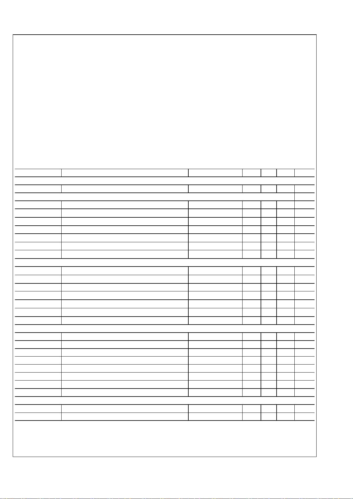
Electrical Characteristics (Note 4) Limits in standard type are for T
J
= 25°C only; limits in boldface type apply
over the junction temperature (TJ) range of -40°C to +125°C. Minimum and Maximum limits are guaranteed through test, design,
or statistical correlation. Typical values represent the most likely parametric norm at TJ = 25°C, and are provided for reference
purposes only. VIN = 48V unless otherwise indicated. (Note 3)
SYMBOL PARAMETER CONDITIONS MIN TYP MAX UNITS
Supply Current
VIN Supply Current Normal Operation 2 3 mA
Detection and Classification
VIN Signature Startup Voltage 1.5 V
Signature Resistance 23.25 24.5 26
kΩ
Signature Resistor Disengage / Classification Engage VIN Rising 11.0 12 12.8 V
Hysteresis 1.9 V
Classification Current Turn Off VIN Rising 22 23.5 25 V
RCLASS Voltage 1.213 1.25 1.287 V
Supply Current During Classification VIN = 17V 0.7 1.1 mA
Line Under Voltage Lock-Out
Default UVLO Release VIN Rising 36 38.5 40 V
Default UVLO Lock out VIN Falling 29.5 31 32.5 V
Default UVLO Hysteresis 6 V
Programmed UVLO Reference Voltage VIN > 12.5V 1.2 1.24 1.28 V
Programmed UVLO Hysteresis Current VIN > UVLO 16 20 24 µA
UVLORTN Pull Down Resistance VIN > 12.5V 55 150
Ω
UVLO Filter 300 µs
Power Good
VDS Required for Power Good Status 1.3 1.5 1.7 V
VDS Hysteresis of Power Good Status 0.8 1 1.2 V
VGS Required for Power Good Status 4.5 5.5 6.5 V
Default Delay Time of Loss-of Power Good Status 30 µs
nPGOOD Current Source 40 55 70 µA
nPGOOD Open circuit Voltage 3.5 4 5.5 V
nPGOOD Pull Down Resistance 180 300
Ω
nPGOOD Threshold 2 2.5 3 V
Shutdown Outputs
nSD/SD Pull Down Resistance 180 300
Ω
Leakage nSD/SD = 16V 1 µA
3 www.national.com
LM5073
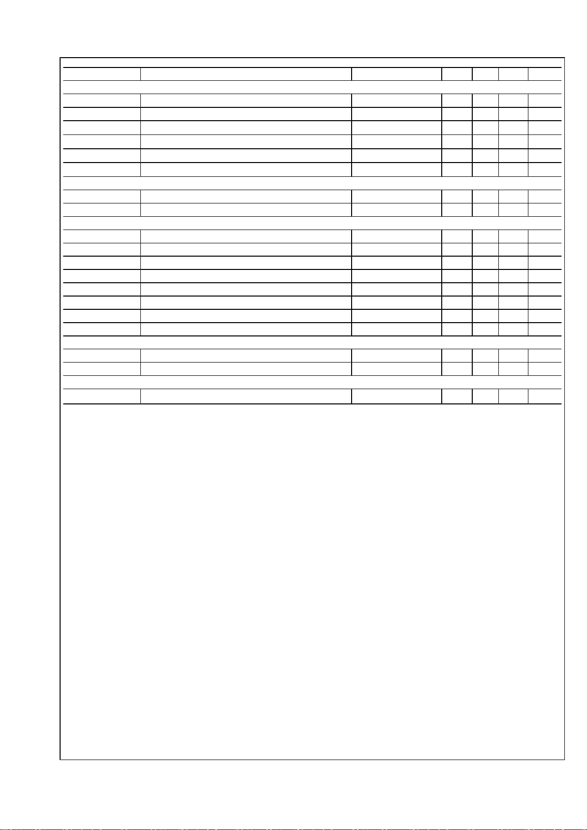
SYMBOL PARAMETER CONDITIONS MIN TYP MAX UNITS
Hot Swap
RDS(ON) Hot Swap MOSFET Resistance 0.7 1.5
Ω
Hot Swap MOSFET Leakage 100 µA
Inrush Current Limit VDS = 4.0V 120 150 180 mA
Default DC Current Limit VDS = 4.0V 380 440 510 mA
High DC Current Limit VDS = 4.0V 690 800 930 mA
Current Limit Programming Accuracy VDS = 4.0V -12 12 %
Hot Swap Over-Voltage Protection
VIN OVP Threshold 60 65 70 V
VIN OVP Threshold, Hysteresis 3 V
Auxiliary Power Option
FAUX Threshold 8.1 8.7 9.5 V
FAUX Hysteresis 0.5 V
FAUX Pull Down Current 50 µA
RAUX Lower Threshold (I = 22 µA) RAUX Pin Rising 2.3 2.7 3.4 V
RAUX Lower Threshold Hysteresis 0.8 V
RAUX Upper Threshold (I = 250 µA) RAUX Pin Rising 5.4 6.2 7.4 V
RAUX Lower Threshold Current 14 22 30 µA
RAUX Upper Threshold Current 170 250 330 µA
PDI Thermal Shutdown (Note 5)
Thermal Shutdown Temperature 165 °C
Thermal Shutdown Hysteresis 20 °C
Thermal Resistance
θ
JA
Junction to Ambient MXA Package 40 °C/W
Note 1: Absolute Maximum Ratings are limits beyond which damage to the device may occur. Operating Ratings are conditions under which operation of the
device is intended to be functional. For guaranteed specifications and test conditions, see the Electrical Characteristics.
Note 2: The human body model is a 100 pF capacitor discharged through a 1.5 kΩ resistor into each pin.
Note 3: For detailed information on soldering the plastic TSSOP package, refer to the Packaging Databook available from National Semiconductor.
Note 4: Minimum and Maximum limits are guaranteed through test, design, or statistical correlation using Statistical Quality Control (SQC) methods. Typical
values represent the most likely parametric norm at TJ = 25°C, and are provided for reference purpose only. Limits are used to calculate National’s Average
Outgoing Quality Level (AOQL).
Note 5: Device thermal limitations may limit usable range.
Note 6: During rear auxiliary operation, the RTN pin can be approximately -0.4V with respect to VEE. This is caused by normal internal bias currents, and will
not harm the device. Application of external voltage or current must not cause the absolute maximum rating to be exceeded.
www.national.com 4
LM5073
Typical Performance Characteristics
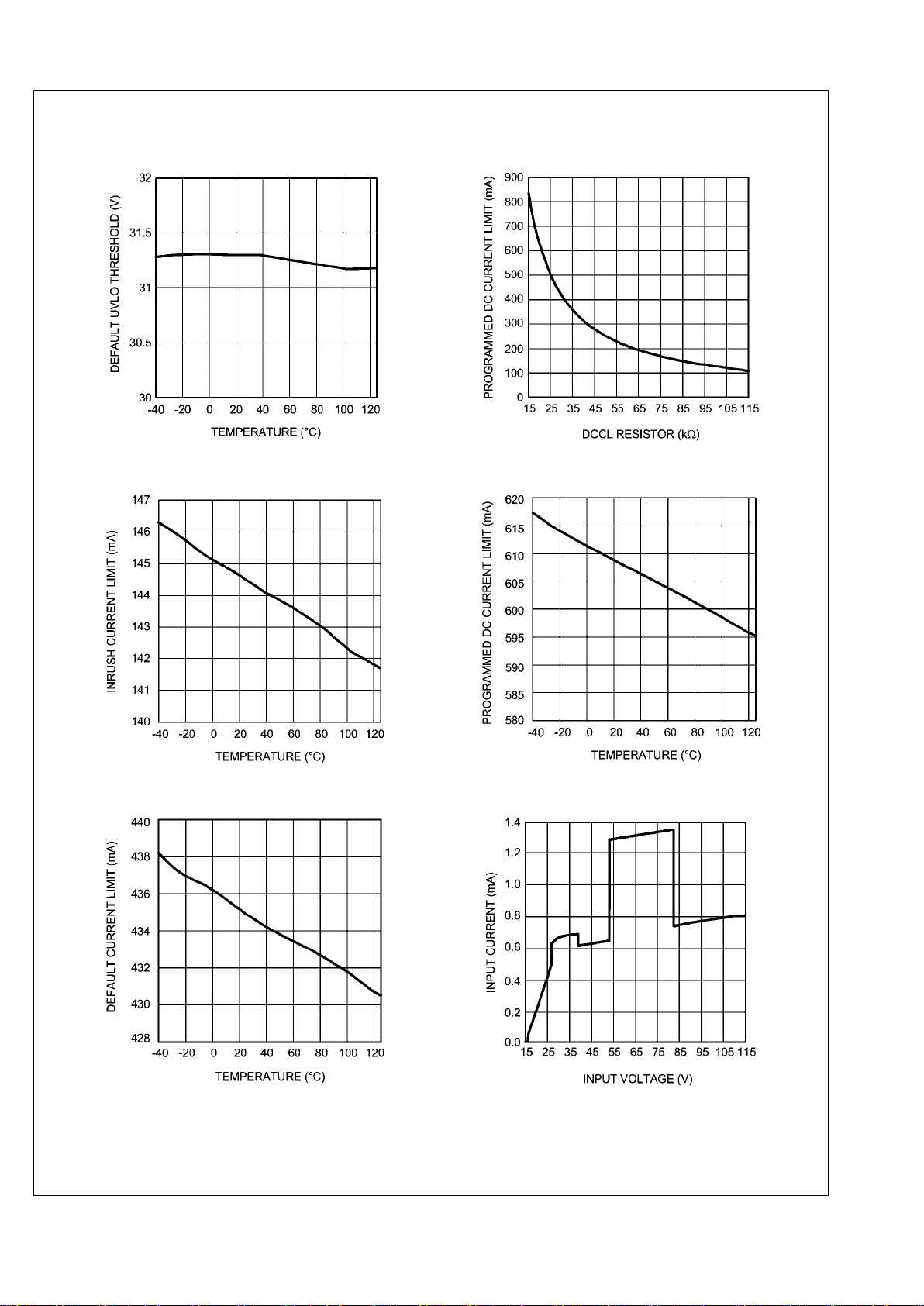
Default UVLO Threshold vs Temperature
30000203
DC Current Limit vs. DCCL Resistor
30000204
Inrush Current Limit vs Temperature
30000205
Programmed DC Current Limit vs Temperature
30000206
Default DC Current Limit vs Temperature
30000207
Input Current vs Input Voltage
30000208
5 www.national.com
LM5073
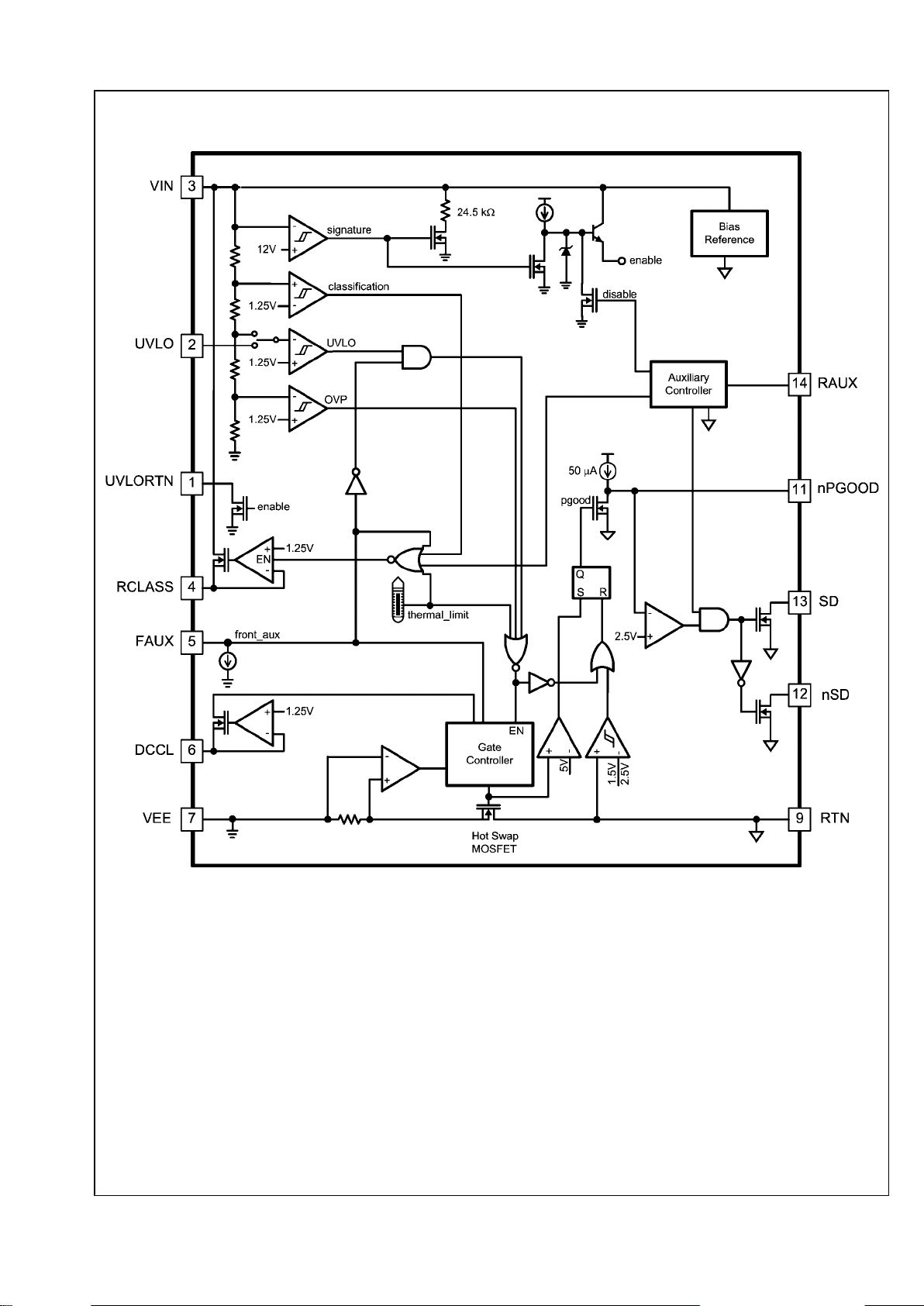
Block Diagram
30000209
FIGURE 1. LM5073 Top Level Block Diagram
Description of Operation and
Applications Information
The LM5073 integrates a fully IEEE 802.3af compliant PD interface with versatile auxiliary power support. When combined with a separate DC-DC converter, it provides a
complete power solution for Powered Devices (PD) that connect to PoE systems.
The LM5073 provides the following features:
1.
The input voltage rating up to 100V allows greater
flexibility when selecting a transient surge suppressor to
protect the PD from voltage transients encountered in
PoE applications.
2.
The integration of the PD signature resistor, inrush
current limit, programmable input voltage under-voltage
lock-out (UVLO), PD classification, and thermal
shutdown simplifies PD implementation.
3.
The PD interface accepts power from auxiliary sources
including AC adapters and solar cells in various
configurations over a wide range of input voltages.
Auxiliary power input can be programmed to be either
non-dominant or dominant over PoE power.
4.
Programmable DC current limit to support PD
applications requiring input currents up to 800 mA.
5.
Complementary open drain outputs for controlling a DCDC converter.
www.national.com 6
LM5073
 Loading...