

NSC LM5072MHX-80, LM5072 Datasheet
August 2006
LM5072
Integrated 100V Power Over Ethernet PD Interface and
PWM Controller with Aux Support
General Description
The LM5072 Powered Device (PD) interface and PulseWidth-Modulation (PWM) controller provides a complete
power solution, fully compliant to IEEE 802.3af, for the PD
connecting into Power over Ethernet (PoE) networks. This
controller integrates all functions necessary to implement
both a PD powered interface and DC-DC converter with a
minimum number of external components. The LM5072 provides the flexibility for the PD to also accept power from
auxiliary sources such as AC adapters in a variety of configurations. The low RDS(ON) PD interface hot swap MOSFET and programmable DC current limit extend the range of
LM5072 applications up to twice the power level of 802.3af
compliant PD devices. The 100V maximum voltage rating
simplifies selection of the transient voltage suppressor that
protects the PD from network transients. The LM5072 includes an easy-to-use PWM controller that facilitates the
various single-ended power supply topologies including the
flyback, forward and buck. The PWM control scheme is
based on peak current mode control, which provides inherent advantages including line feed-forward, cycle-by-cycle
current limit, and simplified feedback loop compensation.
Two versions of the LM5072 provide either an 80% maximum duty cycle (-80 suffix), or a 50% maximum duty cycle
(-50 suffix).
Features
PD Interface
n Fully Compliant IEEE 802.3af PD Interface
n Versatile Auxiliary Power Options
n 9V Minimum Auxiliary Power Operating Range
n 100V Maximum Input Voltage Rating
n Programmable DC Current Limit Up To 800mA
n 100V, 0.7Ω Hot Swap MOSFET
n Integrated PD Signature Resistor
n Integrated PoE Input UVLO
n Programmable Inrush Current Limit
n PD Classification Capability
n Power Good Indicator
n Thermal Shutdown Protection
PWM Controller
n Current Mode PWM Controller
n 100V Start-up Regulator
n Error Amplifier with 2% Voltage Reference
n Supports Isolated and Non-Isolated Applications
n Programmable Oscillator Frequency
n Programmable Soft-Start
n 800 mA Peak Gate Driver
n 80% Maximum Duty Cycle with Built-in Slope
Compensation (-80 device)
n 50% Maximum Duty Cycle, No Slope Compensation
(-50 device)
Applications
n IEEE 802.3af Compliant PoE Powered Devices
n Non-Compliant, Application Specific Devices
n Higher Power Ethernet Powered Devices
Packages
n TSSOP-16 EP (Exposed Pad)
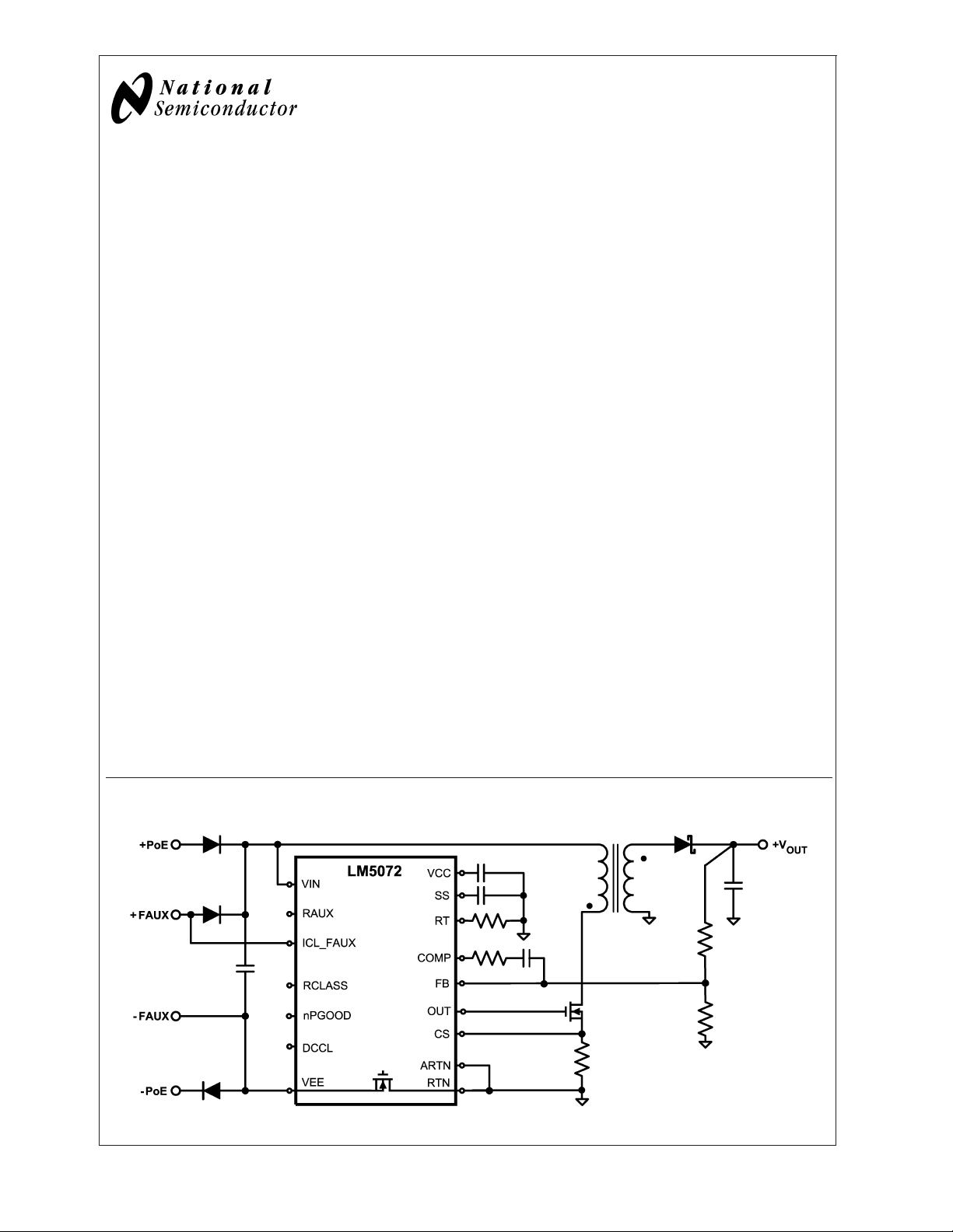
LM5072 Integrated 100V Power Over Ethernet PD Interface and PWM Controller with Aux Support
Simplified Application Diagram
20184601
© 2006 National Semiconductor Corporation DS201846 www.national.com
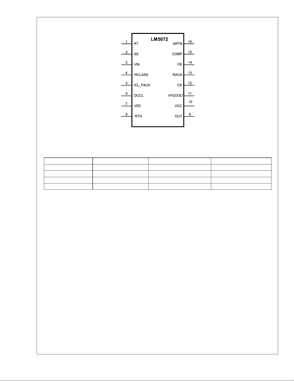
Connection Diagram
LM5072
16 Lead TSSOP-EP
20184602
Ordering Information
Order Number Description NSC Package Type / Drawing Supplied As
LM5072MH-50 50% Duty Cycle Limit TSSOP-16EP/MXA16A 92 units per rail
LM5072MHX-50 50% Duty Cycle Limit TSSOP-16EP/MXA16A 2500 units on tape and reel
LM5072MH-80 80% Duty Cycle Limit TSSOP-16EP/MXA16A 92 units per rail
LM5072MHX-80 80% Duty Cycle Limit TSSOP-16EP/MXA16A 2500 units on tape and reel
www.national.com 2
Pin Descriptions
Pin Number Name Description
1 RT PWM controller oscillator frequency programming pin.
2 SS Soft-start programming pin.
3 VIN Positive supply pin for the PD interface and the internal PWM controller start-up regulator.
4 RCLASS PD classification programming pin.
5 ICL_FAUX Inrush current limit programming pin; also the front auxiliary power enable pin.
6 DCCL PD interface DC current limit programming pin.
7 VEE Negative supply pin for PD interface; connected to PoE and/or front auxiliary power return
path.
8 RTN PWM controller power return; connected to the drain of the internal PD interface hot swap
MOSFET; should be externally connected to the reference ground of the PWM controller.
9 OUT PWM controller gate driver output pin.
10 VCC PWM controller start-up regulator output pin.
11 nPGOOD PD interface Power Good indicator and delay timer pin; active low state indicates PoE
interface is in normal operation.
12 CS PWM controller current sense input pin.
13 RAUX Rear auxiliary power enable pin; can be programmed for auxiliary power dominance over
PoE power.
14 FB PWM controller voltage feedback pin and inverting input of the internal error amplifier;
connect to ARTN to disable the error amplifier in isolated dc-dc converter applications.
15 COMP Output of the internal error amplifier and control input to the PWM comparator. In isolated
applications, COMP is controlled by the secondary side error amplifier via an opto-coupler.
16 ARTN PWM controller reference ground pin; should be shorted externally to the RTN pin as a
single point ground connection to improve noise immunity.
EP Exposed metal pad on the underside of the device. It is recommended to connect this pad to
a PC Board plane connected to the VEE pin to improve heat dissipation.
LM5072
www.national.com3
Absolute Maximum Ratings (Note 1)
If Military/Aerospace specified devices are required,
LM5072
please contact the National Semiconductor Sales Office/
Distributors for availability and specifications.
VIN , RTN to VEE (Note 7) -0.3V to 100V
RAUX to ARTN -0.3V to 100V
ICL_FAUX to VEE -0.3V to 100V
DCCL, RCLASS to VEE -0.3V to 7V
nPGOOD to ARTN -0.3V to 16V
ARTN to RTN -0.3V to 0.3V
VCC, OUT to ARTN -0.3V to 16V
CS, FB, RT to ARTN -0.3V to 7V
COMP, SS to ARTN -0.3V to 5.5V
ESD Rating
Human Body Model (Note 2) 2000V
Lead Soldering Temp. (Note 3)
Wave (4 seconds)
Infrared (10 seconds)
Vapor Phase (75 seconds)
260˚C
240˚C
219˚C
Storage Temperature -55˚C to 150˚C
Junction Temperature 150˚C
Operating Ratings
VINvoltage 9V to 70V
External voltage applied to V
CC
Operating Junction Temperature -40˚C to 125˚C
8V to 15V
Electrical Characteristics (Note 4) Specifications in standard type face are for T
boldface type apply over the full operating junction temperature range. Unless otherwise specified: V
= +25˚C and those in
J
= 48V, F
IN
OSC
=
250kHz.
SYMBOL PARAMETER CONDITIONS MIN TYP MAX UNITS
Detection and Classification
V
Signature Startup Voltage 1.5 V
IN
Signature Resistance 23.25 24.5 26 kΩ
Signature Resistor Disengage/
V
Rising 11.0 12.0 12.6 V
IN
Classification Engage
Hysteresis 1.9 V
Classification Current Turn Off V
Rising 22 23.5 25 V
IN
Classification Voltage 1.213 1.25 1.287 V
Supply Current During Classification V
= 17V 0.7 1.1 mA
IN
Line Under Voltage Lock-Out
UVLO Release V
UVLO Lock out V
Rising 36 38.5 40 V
IN
Falling 29.5 31.0 32.5 V
IN
UVLO Hysteresis 6 V
UVLO Filter 300 µs
Power Good
VDS Required for Power Good Status 1.3 1.5 1.7 V
VDS Hysteresis of Power Good Status 0.8 1.0 1.2 V
VGS Required for Power Good Status 4.5 5.5 6.5 V
Default Delay Time of Loss-of Power
30 µs
Good Status
nPGOOD current Source 45 55 65 µA
nPGOOD Pull Down Resistance 130 250 Ω
nPGOOD Threshold 2.3 2.5 2.7 V
Hot Swap
RDS(ON) Hot Swap MOSFET Resistance 0.7 1.2 Ω
Hot Swap MOSFET Leakage 110 µA
Default Inrush Current Limit V
Default DC Current Limit V
Front Auxiliary DC Current Limit V
Inrush Current Limit Programming
= 4.0V 120 150 180 mA
DS
= 4.0V 380 440 510 mA
DS
= 4.0V 470 540 610 mA
DS
V
= 4.0V -15 15 %
DS
Accuracy
DC Current Limit Programming Accuracy VDS= 4.0V -12 12 %
www.national.com 4
LM5072
Electrical Characteristics (Note 4) Specifications in standard type face are for T
boldface type apply over the full operating junction temperature range. Unless otherwise specified: V
= +25˚C and those in
J
= 48V, F
IN
OSC
=
250kHz. (Continued)
SYMBOL PARAMETER CONDITIONS MIN TYP MAX UNITS
Auxiliary Power Option
ICL_FAUX Threshold ICL_FAUX Pin Rising 8.1 8.7 9.3 V
ICL_FAUX Pull Down Current 50 µA
RAUX Lower Threshold (I = 22 µA) RAUX Pin Rising 2.3 2.5 3.0 V
RAUX Lower Threshold Hysteresis 0.8 V
RAUX Upper Threshold (I = 250 µA) RAUX Pin Rising 5.4 6.0 6.9 V
RAUX Lower Threshold Current 16 22 28 µA
RAUX Upper Threshold Current 187 250 313 µA
VCC Regulator
VccReg VCC Regulation (VccReg) 7.4 7.7 8 V
VCC Current Limit 15 mA
VCC UVLO (Rising) VccReg
– 210
mV
VccReg
– 100
mV
VCC UVLO (Falling) 5.9 6.2 6.5 V
VIN Supply Current V
Supply Current (Icc) V
VCC Regulator Dropout V
= 10V 2.0 mA
CC
= 10V 3 mA
CC
IN–VCC
(Note 6) 6.5 V
Error Amplifier
Gain Bandwidth 3 MHz
DC Gain 67 dB
Input Voltage 1.225 1.275 V
COMP Sink Capability 5 10 mA
Current Limit
ILIM Delay to Output 30 ns
Cycle by Cycle Current Limit Threshold
0.45 0.5 0.55 V
Voltage
Leading Edge Blanking Time 65 ns
CS Sink Impedance (clocked) 35 55 Ω
Soft-start
Soft-start Current Source 8 10 12 µA
Oscillator
Frequency1 (R
Frequency2 (R
= 26.1 kΩ) 175 200 225 KHz
T
= 8.7 kΩ) 515 580 645 KHz
T
Sync threshold 2.6 3.2 3.8 V
PWM Comparator
Delay to Output 25 ns
Min Duty Cycle 0 %
Max Duty Cycle (-80 Device) 75 80 85 %
Max Duty Cycle (-50 Device) 47 50 53 %
COMP to PWM Comparator Gain 0.33
COMP Open Circuit Voltage 4.3 5.2 6.1 V
COMP Short Circuit Current 0.6 1.0 1.4 mA
Slope Compensation (LM5072-80 Device Only)
Slope Comp Amplitude 70 90 110 mV
Output Section
Output High Saturation 0.25 0.75 V
mV
www.national.com5
Electrical Characteristics (Note 4) Specifications in standard type face are for T
boldface type apply over the full operating junction temperature range. Unless otherwise specified: V
LM5072
250kHz. (Continued)
= +25˚C and those in
J
= 48V, F
IN
SYMBOL PARAMETER CONDITIONS MIN TYP MAX UNITS
Output Low Saturation 0.25 0.75 V
t
r
t
f
Rise time C
Fall time C
= 1nF 18 ns
LOAD
= 1nF 15 ns
LOAD
PDI Thermal Shutdown (Note 5)
Thermal Shutdown Temp. 165 ˚C
Thermal Shutdown Hysteresis 25 ˚C
Thermal Resistance
θ
JA
Note 1: Absolute Maximum Ratings are limits beyond which damage to the device may occur. Operating Ratings are conditions under which operation of the device
is intended to be functional. For guaranteed specifications and test conditions, see the Electrical Characteristics.
Note 2: The human body model is a 100 pF capacitor discharged through a 1.5 kΩ resistor into each pin.
Note 3: For detailed information on soldering the plastic TSSOP package, refer to the Packaging Databook available from National Semiconductor.
Note 4: Minimum and Maximum limits are guaranteed through test, design, or statistical correlation using Statistical Quality Control (SQC) methods. Typical values
represent the most likely parametric norm at T
Level (AOQL).
Note 5: Device thermal limitations may limit usable range.
Note 6: The VCC regulator is intended for use solely as a bias supply for the LM5072, dropout assumes 3mA of external V
Note 7: During rear auxiliary operation, the RTN pin can be approximately -0.4V with respect to VEE. This is caused by normal internal bias currents, and will not
harm the device. Application of external voltage or current must not cause the absolute maximum rating to be exceeded.
Junction to Ambient MXA package 40 ˚C/W
= 25˚C, and are provided for reference purpose only. Limits are used to calculate National’s Average Outgoing Quality
J
current.
CC
OSC
=
www.national.com 6
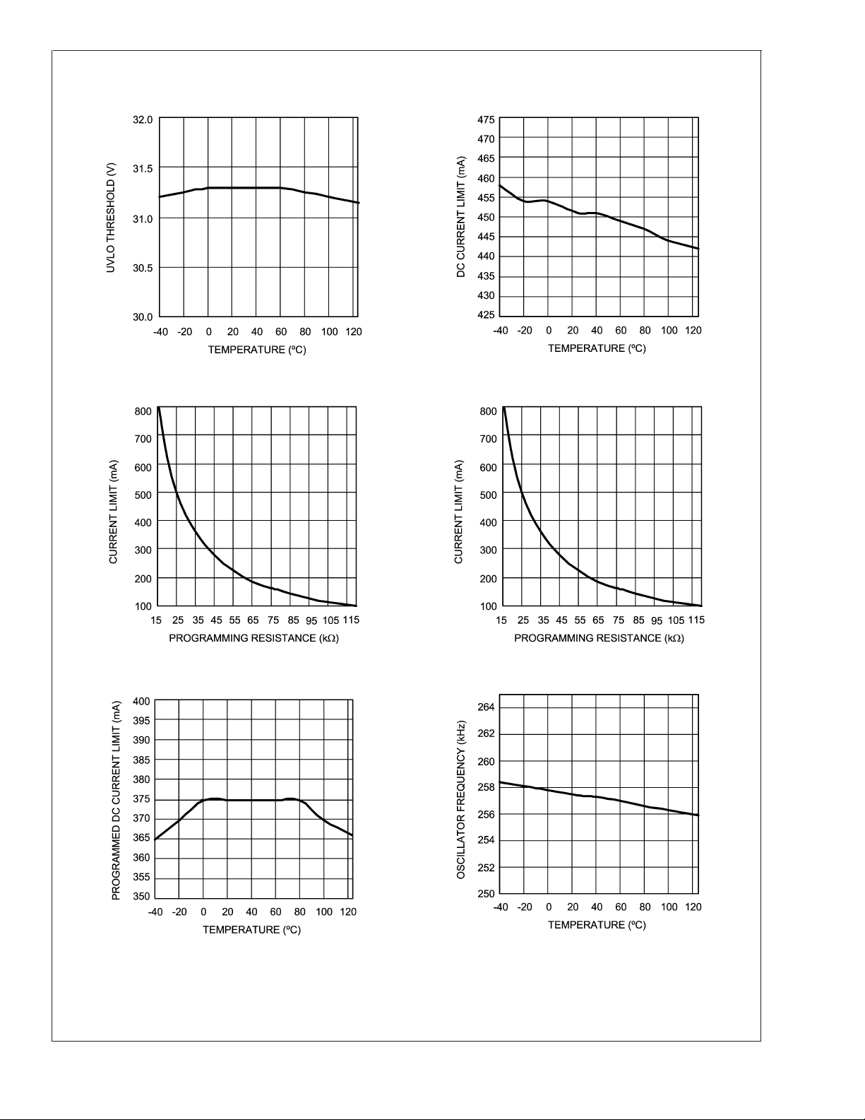
Typical Performance Characteristics
UVLO Threshold vs Temperature Default Current Limit vs Temperature
LM5072
20184603
20184604
Inrush Current Limit vs ICL_FAUX Resistor DC Current Limit vs. DCCL Resistor
20184605 20184606
Programmed DC Current Limit vs Temperature Oscillator Frequency vs Temperature
20184607
20184608
www.national.com7
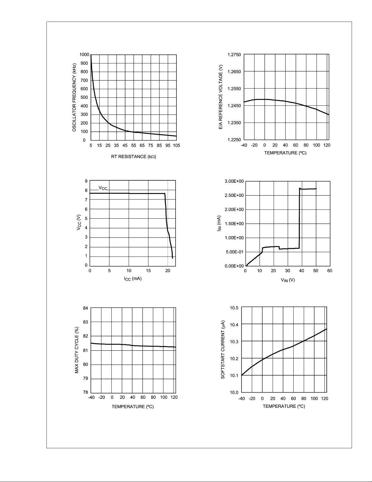
Typical Performance Characteristics (Continued)
LM5072
Oscillator Frequency vs RT Resistance Error Amplifier Reference Voltage vs Temperature
20184610
VCCvs I
20184609
CC
Input Current vs Input Voltage
20184611
Maximum Duty Cycle vs Temperature Soft-start Current vs Temperature
20184613
www.national.com 8
20184612
20184614
 Loading...