

NSC LM5041MTCX, LM5041MTC Datasheet
LM5041
Cascaded PWM Controller
General Description
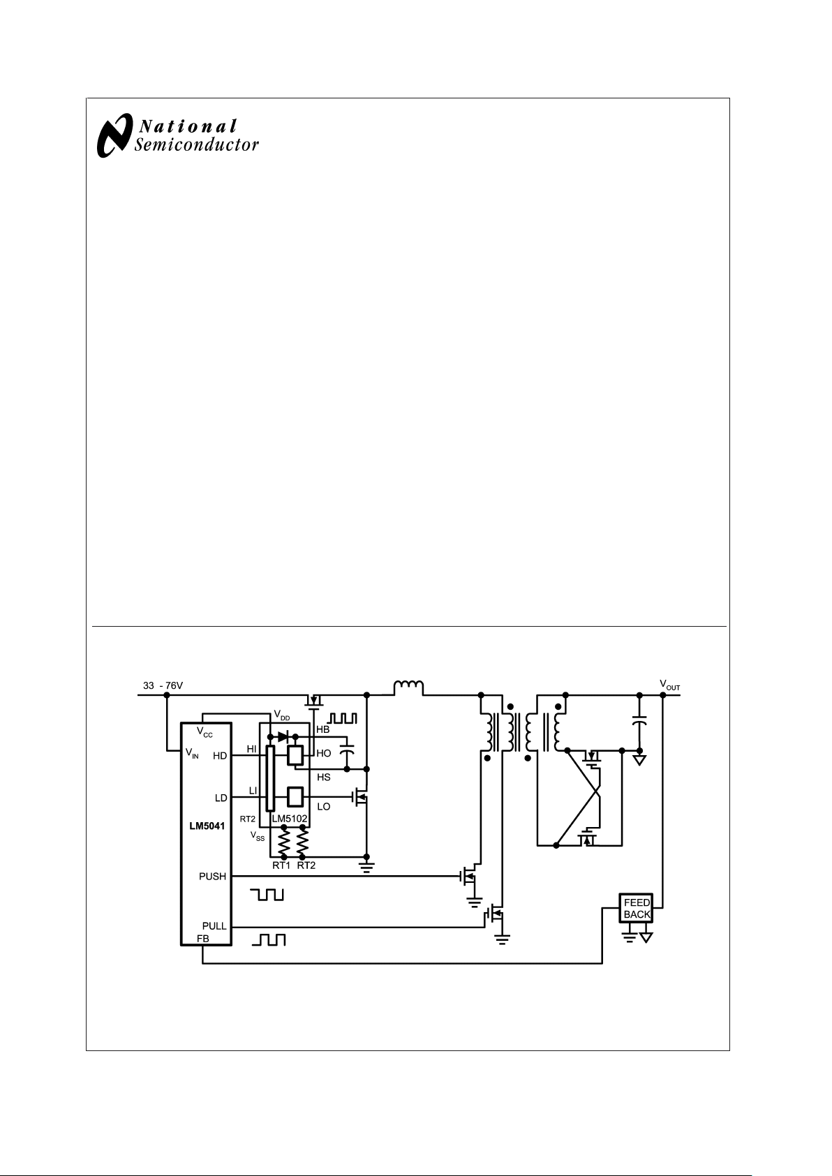
The LM5041 PWM controller contains all of the features
necessary to implement either current-fed or voltage-fed
push-pull or bridge power converters. These “Cascaded”
topologies are well suited for multiple output and higher
power applications. The LM5041’s four control outputs include: the buck stage controls (HD and LD) and the pushpull control outputs (PUSH and PULL). Push-pull outputs are
driven at 50% nominal duty cycle at one half of the switching
frequency of the buck stage and can be configured for either
a guaranteed overlap time (for current-fed applications) or a
guaranteed both-off time (for voltage-fed applications).
Push-pull stage MOSFETs can be driven directly from the
internal gate drivers while the buck stage requires an external driver such as the LM5102. The LM5041 includes a
high-voltage start-up regulator that operates over a wide
input range of 15V to 100V. The PWM controller is designed
for high-speed capability including an oscillator frequency
range up to 1 MHz and total propagation delays of less than
100ns. Additional features include: line Under-Voltage Lockout (UVLO), soft-start, an error amplifier, precision voltage
reference, and thermal shutdown.
Features
n Internal Start-up Bias Regulator
n Programmable Line Under-Voltage Lockout (UVLO) with
Adjustable Hysteresis
n Current Mode Control
n Internal Error Amplifier with Reference
n Dual Mode Over-Current Protection
n Leading Edge Blanking
n Programmable Push-Pull Overlap or Dead Time
n Internal 1.5A Push-Pull Gate Drivers
n Programmable Soft-start
n Programmable Oscillator with Sync Capability
n Precision Reference
n Thermal Shutdown
Applications
n Telecommunication Power Converters
n Industrial Power Converters
n Multi-Output Power Converters
n +42V Automotive Systems
Packages
n TSSOP-16
n LLP-16 (5x5 mm) Thermally Enhanced
Typical Application Circuit
20074901
Simplified Cascaded Push-Pull Power Converter
August 2003
LM5041 Cascaded PWM Controller
© 2003 National Semiconductor Corporation DS200749 www.national.com
Connection Diagram
20074902
16-Lead TSSOP, LLP
Ordering Information
Order Number Package Type NSC Package Drawing Supplied As
LM5041MTC TSSOP-16 MTC-16 92 Units per anti-static tube
LM5041MTCX TSSOP-16 MTC-16 2500 Units on Tape and Reel
LM5041SD LLP-16 SDA-16A Available Soon
LM5041SDX LLP-16 SDA-16A Available Soon
Pin Description
PIN NAME DESCRIPTION APPLICATION INFORMATION
1V
IN
Source Input Voltage Input to start-up regulator. Input range 15V to 100V.
2 FB Feedback Signal Inverting input for the internal error amplifier. The
non-inverting input is connected to a 0.75V
reference.
3 COMP Output of the Internal Error Amplifier There is an internal 5kΩ resistor pull-up on this pin.
The error amplifier provides an active sink.
4 REF Precision 5 volt reference output Maximum output current: 10mA. Locally decouple
with a 0.1µF capacitor. Reference stays low until the
line UV and the V
CC
UV are satisfied.
5 HD Main Buck PWM control output Buck switch PWM control output. The maximum duty
cycle clamp for this output corresponds to an off time
of typically 240ns per cycle. The LM5101 or LM5102
Buck stage gate driver can be used to level shift and
drive the Buck switch.
6 LD Sync Switch control output Sync Switch control output. Inversion of HD output.
The LM5101 or LM5102 lower drive can be used to
drive the synchronous rectifier switch.
7V
CC
Output from the internal high voltage start-up
regulator. Regulated to 9 volts.
If an auxiliary winding raises the voltage on this pin
above the regulation setpoint, the internal start-up
regulator will shutdown, reducing the IC power
dissipation.
8 PUSH Output of the push-pull drivers Output of the push-pull gate driver. Output capability
of 1.5A peak .
LM5041
www.national.com 2
Pin Description (Continued)
PIN NAME DESCRIPTION APPLICATION INFORMATION
9 PULL Output of the push-pull drivers Output of the push-pull gate driver. Output capability
of 1.5A peak.
10 PGND Power ground Connect directly to analog ground.
11 AGND Analog ground Connect directly to power ground.
12 CS Current sense input Current sense input to the PWM comparator (CM
control). There is a 50ns leading edge blanking on
this pin. Using separate dedicated comparators, if
CS exceeds 0.5V the outputs will go into cycle by
cycle current limit. If CS exceeds 0.6V the outputs
will be disabled and a soft-start commenced.
13 SS Soft-start control An external capacitor and an internal 10uA current
source, set the soft-start ramp. The controller will
enter a low power state if the SS pin is below the
shutdown threshold of 0.45V
14 TIME Push-Pull overlap and dead time control An external resistor sets the overlap time or dead
time for the push-pull outputs. A resistor connected
between TIME and GND produces overlap. A
resistor connected between TIME and REF produces
dead time.
15 RT / SYNC Oscillator timing resistor pin and sync An external resistor sets the oscillator frequency.
This pin will also accept an external oscillator.
16 UVLO Line Under-Voltage Shutdown An external divider from the power converter source
sets the shutdown levels. Threshold of operation
equals 2.5V. Hysteresis is set by a switched internal
current source (20µA).
LM5041
www.national.com3
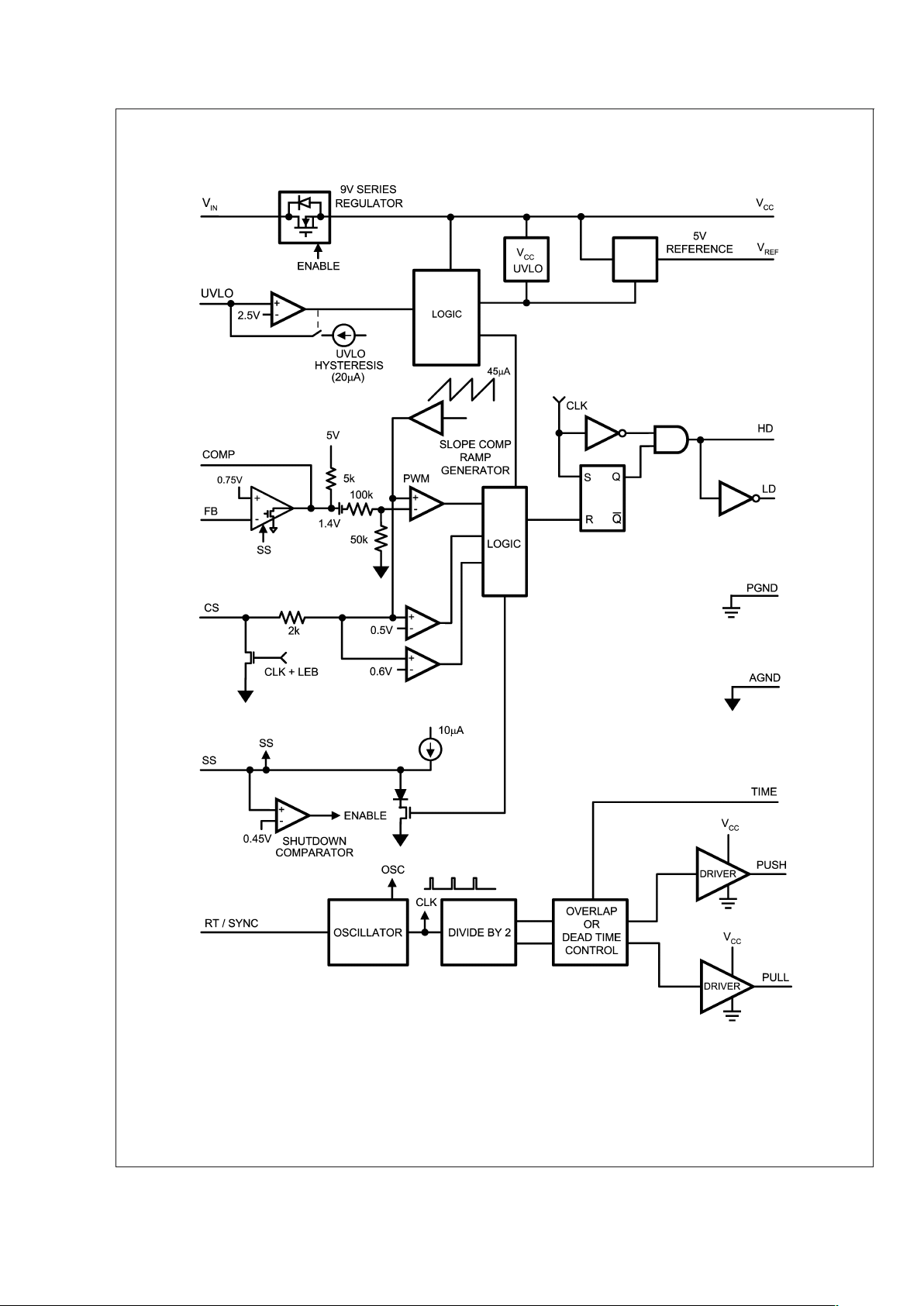
Block Diagram
Simplified Block Diagram
20074903
LM5041
www.national.com 4
Absolute Maximum Ratings (Note 1)
If Military/Aerospace specified devices are required,
please contact the National Semiconductor Sales Office/
Distributors for availability and specifications.
V
IN
to GND 100V
V
CC
to GND 16V
All Other Inputs to GND -0.3 to 7V
Junction Temperature 150˚C
Storage Temperature
Range
-65˚C to +150˚C
ESD Rating 2 kV
Lead temperature (Note 2)
Wave 4 seconds 260˚C
Infrared 10 seconds 240˚C
Vapor Phase 75 seconds 219˚C
Operating Ratings (Note 1)
V
IN
15 to 90V
Junction Temperature -40˚C to +105˚C
Electrical Characteristics
Specifications with standard typeface are for TJ= 25˚C, and those with boldface type apply over full Operating Junction
Temperature range.V
IN
= 48V, VCC= 10V, RT = 26.7kΩ,R
SET
= 20kΩ) unless otherwise stated (Note 3)
Symbol Parameter Conditions Min Typ Max Units
Startup Regulator
V
CC
Reg VCCRegulation open circuit 8.7 9 9.3 V
V
CC
Current Limit (Note 4) 15 25 mA
I-V
IN
Startup Regulator
Leakage (external Vcc
Supply)
V
IN
= 100V 145 500 µA
Shutdown Current (Iin) UVLO = 0V, V
CC
= open 350 450 µA
V
CC
Supply
V
CC
Under-voltage
Lockout Voltage
(positive going V
cc
)
V
CC
Reg
- 400mV
VCCReg -
275mV
V
V
CC
Under-voltage
Hysteresis
1.7 2.1 2.6 V
Supply Current (ICC)CL=0 3 4 mA
Error Amplifier
GBW Gain Bandwidth 3 MHz
DC Gain 80 dB
Input Voltage V
FB
= COMP 0.735 0.75 0.765 V
COMP Sink Capability V
FB
= 1.5V, COMP= 1V 4 8mA
Reference Supply
V
REF
Ref Voltage I
REF
=0mA 4.85 5 5.15 V
Ref Voltage
Regulation
I
REF
= 0 to 10mA 25 50 mV
Ref Current Limit 15 20 mA
Current Limit
ILIM Delay to Output CS Step from 0 to 0.6V
Time to Onset of OUT
Transition (90%)
C
L
=0
40 ns
Cycle by Cycle
Threshold Voltage
0.45 0.5 0.55 V
Cycle Skip Threshold
Voltage
Resets SS capacitor;
auto restart
0.55 0.6 0.65 V
Leading Edge
Blanking Time
50 ns
CS Sink Current
(clocked)
CS = 0.3V 25 mA
LM5041
www.national.com5
 Loading...