NSC LM5022MM, LM5022 Datasheet
January 2007
LM5022
60V Low Side Controller for Boost and SEPIC
General Description
The LM5022 is a high voltage low-side N-channel MOSFET
controller ideal for use in boost and SEPIC regulators. It contains all of the features needed to implement single ended
primary topologies. Output voltage regulation is based on
current-mode control, which eases the design of loop compensation while providing inherent input voltage feed-forward.
The LM5022 includes a start-up regulator that operates over
a wide input range of 6V to 60V. The PWM controller is designed for high speed capability including an oscillator frequency range up to 2 MHz and total propagation delays less
than 100 ns. Additional features include an error amplifier,
precision reference, line under-voltage lockout, cycle-by-cycle current limit, slope compensation, soft-start, external synchronization capability and thermal shutdown. The LM5022 is
available in the MSOP-10 package.
Features
■
Internal 60V Startup Regulator
■
1A Peak MOSFET Gate Driver
■
VIN Range 6V to 60V
■
Duty Cycle Limit of 90%
■
Programmable UVLO with Hysteresis
■
Cycle-by-Cycle Current Limit
■
External Synchronizable (AC-coupled)
■
Single Resistor Oscillator Frequency Set
■
Slope Compensation
■
Adjustable Soft-start
■
MSOP-10 Package
Applications
■
Boost Converter
■
SEPIC Converter
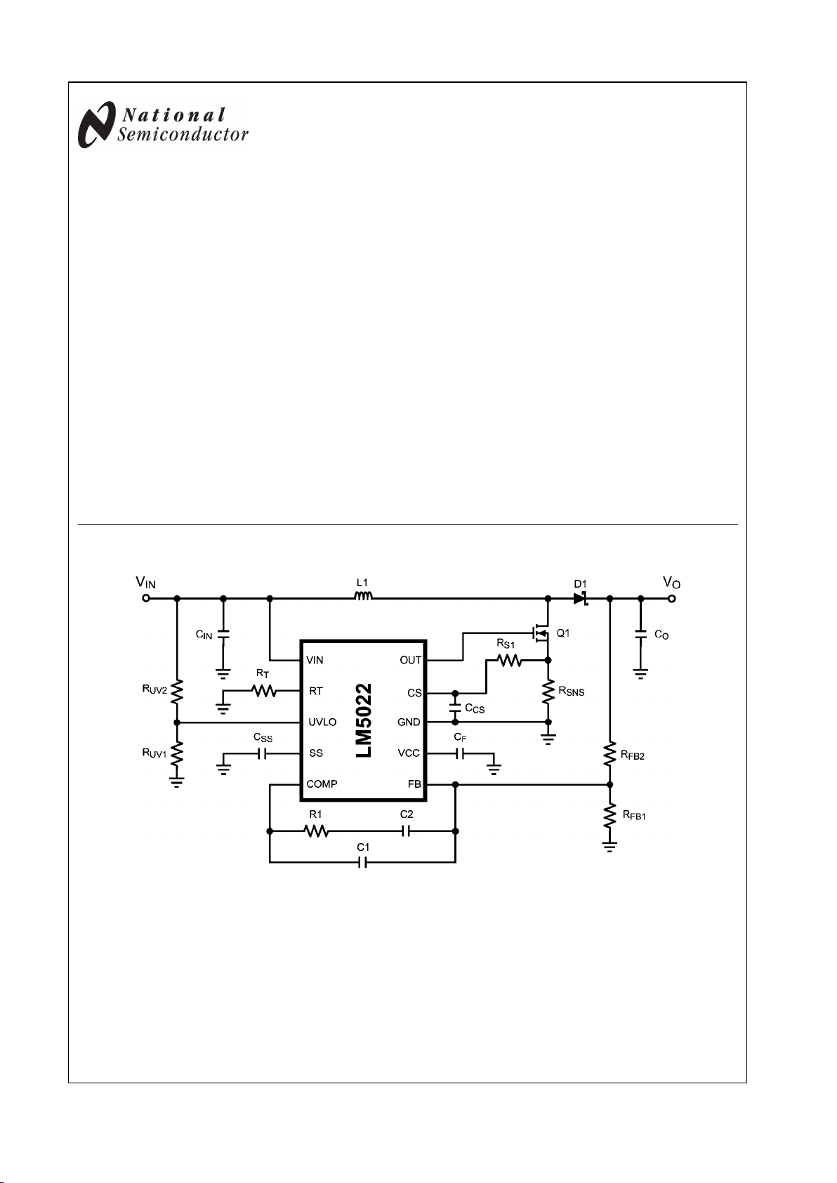
Typical Application
20212201
© 2007 National Semiconductor Corporation 202122 www.national.com
LM5022 60V Low Side Controller for Boost and SEPIC
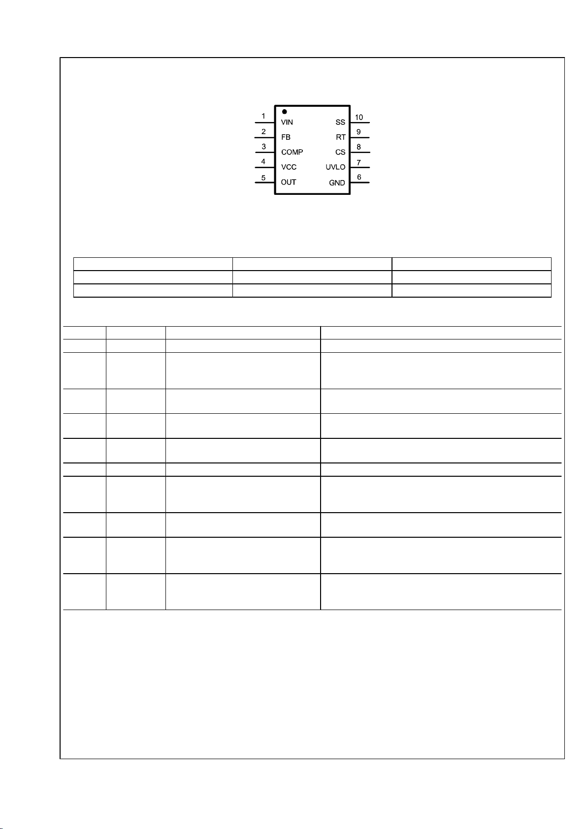
Connection Diagram
20212253
10-Lead MSOP
NS Package Number MUB10A
Ordering Information
Part Number NS Package Drawing Supplied As
LM5022MM MUB10A 1000 Units on Tape and Reel
LM5022MMX MUB10A 3500 Units on Tape and Reel
Pin Descriptions
Pin(s) Name Description Application Information
1 VIN Source input voltage Input to the start-up regulator. Operates from 6V to 60V.
2 FB Feedback pin
Inverting input to the internal voltage error amplifier. The noninverting input of the error amplifier connects to a 1.25V
reference.
3 COMP
Error amplifier output and PWM
comparator input
The control loop compensation components connect between
this pin and the FB pin.
4 VCC
Output of the internal, high voltage linear
regulator.
This pin should be bypassed to the GND pin with a ceramic
capacitor.
5 OUT Output of MOSFET gate driver Connect this pin to the gate of the external MOSFET. The gate
driver has a 1A peak current capability.
6 GND System ground
7 UVLO Input Under-Voltage Lock-out
Set the start-up and shutdown levels by connecting this pin to the
input voltage through a resistor divider. A 20 µA current source
provides hysteresis.
8 CS
Current Sense input Input for the switch current used for current mode control and for
current limiting.
9 RT/SYNC
Oscillator frequency adjust pin and
synchronization input
An external resistor connected from this pin to GND sets the
oscillator frequency. This pin can also accept an AC-coupled
input for synchronization from an external clock.
10 SS Soft-start pin
An external capacitor placed from this pin to ground will be
charged by a 10 µA current source, creating a ramp voltage to
control the regulator start-up.
www.national.com 2
LM5022
Absolute Maximum Ratings (Note 1)
If Military/Aerospace specified devices are required,
please contact the National Semiconductor Sales Office/
Distributors for availability and specifications.
VIN to GND -0.3V to 65V
VCC to GND -0.3V to 16V
RT/SYNC to GND -0.3V to 5.5V
OUT to GND -1.5V for < 100 ns
All other pins to GND -0.3V to 7V
Power Dissipation Internally Limited
Junction Temperature 150°C
Storage Temperature -65°C to +150°C
Soldering Information
Vapor Phase (60 sec.) 215°C
Infrared (15 sec.) 220°C
ESD Rating
Human Body Model (Note 2) 2 kV
Operating Ranges (Note 4)
Supply Voltage 6V to 60V
External Volatge at V
CC
7.5V to 14V
Junction Temperature Range -40°C to +125°C
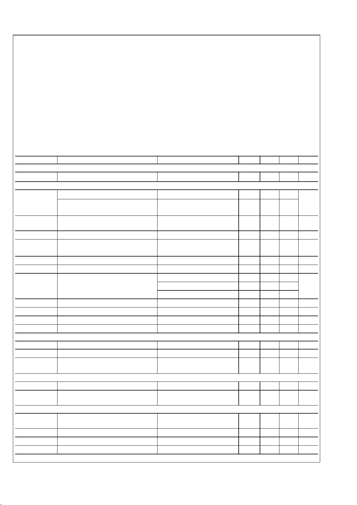
Electrical Characteristics Limits in standard type are for T
J
= 25°C only; limits in boldface type apply over the
junction temperature (TJ) range of -40°C to +125°C. Minimum and Maximum limits are guaranteed through test, design, or statistical
correlation. Typical values represent the most likely parametric norm at TJ = 25°C, and are provided for reference purposes only.
VIN = 24V and RT = 27.4 kΩ unless otherwise indicated. (Note 3)
Symbol Parameter Conditions Min Typ Max Units
SYSTEM PARAMETERS
V
FB
FB Pin Voltage
-40°C ≤ T
J
≤ 125°C
1.225 1.250 1.275 V
START-UP REGULATOR
VCC
VCC Regulation
9V ≤ VIN ≤ 60V, ICC = 1 mA
6.6 7 7.4
V
VCC Regulation
6V ≤ VIN < 9V, VCC Pin Open
Circuit
5
I
CC
Supply Current
OUT Pin Capacitance = 0
VCC = 10V
3.5 4
mA
I
CC-LIM
VCC Current Limit VCC = 0V, (Note 4, 6) 15 35 mA
VIN - VCC
Dropout Voltage Across Bypass Switch
ICC = 0 mA, fSW < 200 kHz
6V ≤ VIN ≤ 8.5V
200
mV
V
BYP-HI
Bypass Switch Turn-off Threshold VIN increasing 8.7 V
V
BYP-HYS
Bypass Switch Threshold Hysteresis VIN Decreasing 260 mV
Z
VCC
VCC Pin Output Impedance
0 mA ≤ ICC ≤ 5 mA
VIN = 6.0V 58
Ω
VIN = 8.0V 53
VIN = 24.0V 1.6
VCC
-HI
VCC Pin UVLO Rising Threshold 5 V
VCC
-HYS
VCC Pin UVLO Falling Hysteresis 300 mV
I
VIN
Start-up Regulator Leakage VIN = 60V 150 500 µA
I
IN-SD
Shutdown Current V
UVLO
= 0V, VCC = Open Circuit 350 450 µA
ERROR AMPLIFIER
GBW Gain Bandwidth 4 MHz
A
DC
DC Gain 75 dB
I
COMP
COMP Pin Current Sink Capability
VFB = 1.5V
V
COMP
= 1V
5 17
mA
UVLO
V
SD
Shutdown Threshold 1.22 1.25 1.28 V
I
SD-HYS
Shutdown
Hysteresis Current Source
16 20 24
µA
CURRENT LIMIT
t
LIM-DLY
Delay from ILIM to Output
CS steps from 0V to 0.6V
OUT transitions to 90% of VCC
30
ns
V
CS
Current Limit Threshold Voltage 0.45 0.5 0.55 V
t
BLK
Leading Edge Blanking Time 65 ns
R
CS
CS Pin Sink Impedance Blanking active 40 75
Ω
3 www.national.com
LM5022
Symbol Parameter Conditions Min Typ Max Units
SOFT-START
I
SS
Soft-start Current Source 7 10 13 µA
V
SS-OFF
Soft-start to COMP Offset 0.35 0.55 0.75 V
OSCILLATOR
f
SW
RT to GND = 84.5 kΩ
(Note 5) 170 200 230 kHz
RT to GND = 27.4 kΩ
(Note 5) 525 600 675 kHz
RT to GND = 16.2 kΩ
(Note 5) 865 990 1115 kHz
V
SYNC-HI
Synchronization Rising Threshold 3.8 V
PWM COMPARATOR
t
COMP-DLY
Delay from COMP to OUT Transition
V
COMP
= 2V
CS stepped from 0V to 0.4V
25
ns
D
MIN
Minimum Duty Cycle V
COMP
= 0V 0 %
D
MAX
Maximum Duty Cycle 90 95 %
A
PWM
COMP to PWM Comparator Gain 0.33 V/V
V
COMP-OC
COMP Pin Open Circuit Voltage VFB = 0V 4.3 5.2 6.1 V
I
COMP-SC
COMP Pin Short Circuit Current V
COMP
= 0V, VFB = 1.5V 0.6 1.1 1.5 mA
SLOPE COMPENSATION
V
SLOPE
Slope Compensation Amplitude 80 105 130 mV
MOSFET DRIVER
V
SAT-HI
Output High Saturation Voltage (VCC –
VOUT)
I
OUT
= 50 mA 0.25 0.75 V
V
SAT-LO
Output Low Saturation Voltage (VOUT) I
OUT
= 100 mA 0.25 0.75 V
t
RISE
OUT Pin Rise Time OUT Pin load = 1 nF 18 ns
t
FALL
OUT Pin Fall Time OUT Pin load = 1 nF 15 ns
THERMAL CHARACTERISTICS
T
SD
Thermal Shutdown Threshold 165 °C
T
SD-HYS
Thermal Shutdown Hysteresis 25 °C
θ
JA
Junction to Ambient Thermal Resistance MUB-10A Package 200 °C/W
Note 1: Absolute Maximum Ratings are limits beyond which damage to the device may occur. The Recommended Operating Limits define the conditions within
which the device is intended to be functional. For guaranteed specifications and test conditions, see the Electrical Characteristics.
Note 2: The human body model is a 100 pF capacitor discharged through a 1.5kΩ resistor into each pin.
Note 3: Min and Max limits are 100% production tested at 25°C. Limits over the operating temperature range are guaranteed through correlation using Statistical
Quality Control (SQC) methods. Limits are used to calculate National’s Average Outgoing Quality Level (AOQL).
Note 4: Device thermal limitations may limit usable range.
Note 5: Specification applies to the oscillator frequency.
Note 6: VCC provides bias for the internal gate drive and control circuits.
www.national.com 4
LM5022
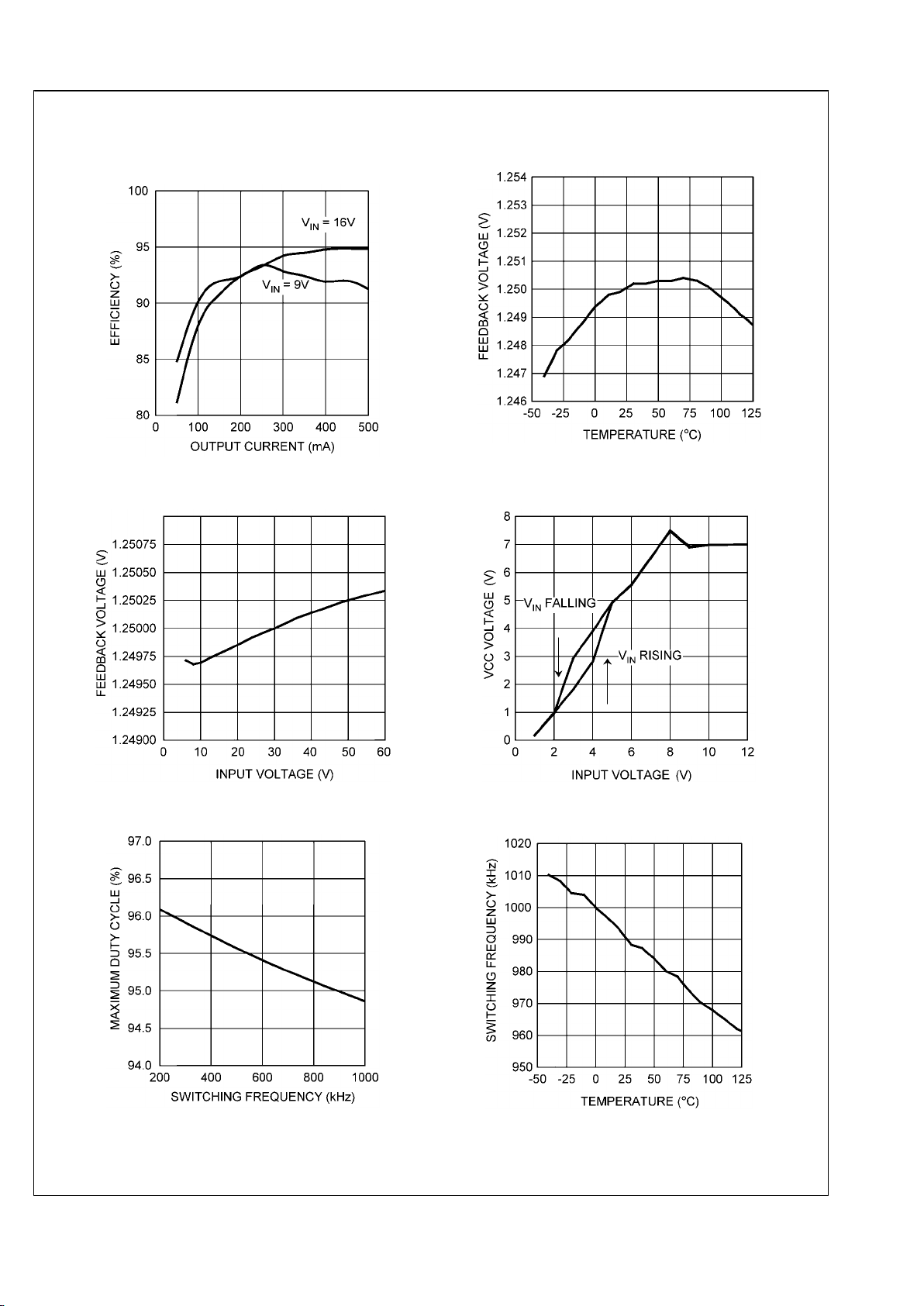
Typical Performance Characteristics
Efficiency, VO = 40V
Example Circuit BOM
20212255
VFB vs. Temp (VIN = 24V)
20212203
VFB vs. VIN (TA = 25°C)
20212204
VCC vs. VIN (TA = 25°C)
20212205
Max Duty Cycle vs. fSW (TA = 25°C)
20212206
fSW vs. Temperature (RT = 16.2 kΩ)
20212207
5 www.national.com
LM5022
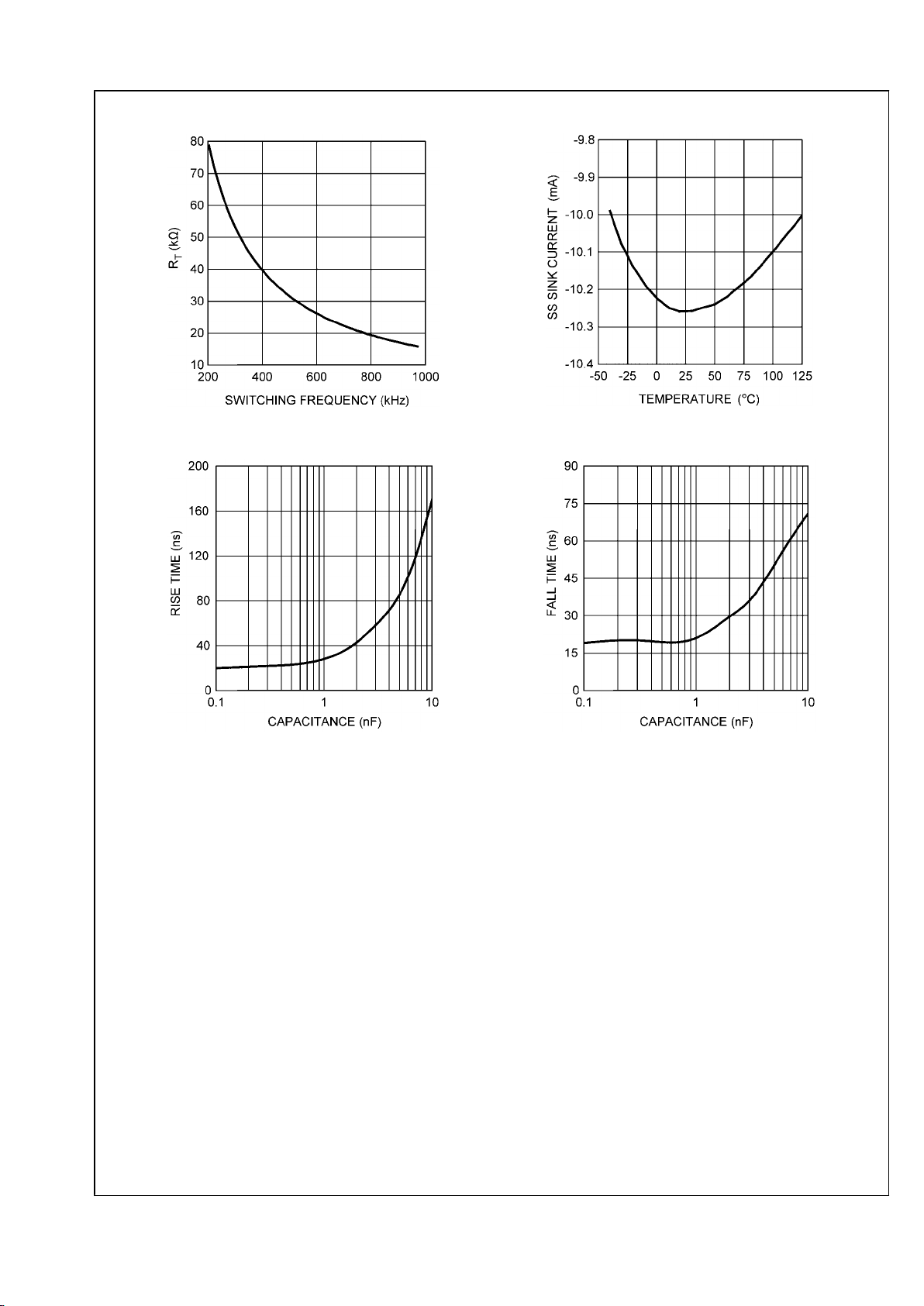
RT vs. fSW (TA = 25°C)
20212208
SS vs. Temperature
20212209
OUT Pin t
RISE
vs. Gate Capacitance
20212210
OUT Pin t
FALL
vs. Gate Capacitance
20212211
www.national.com 6
LM5022
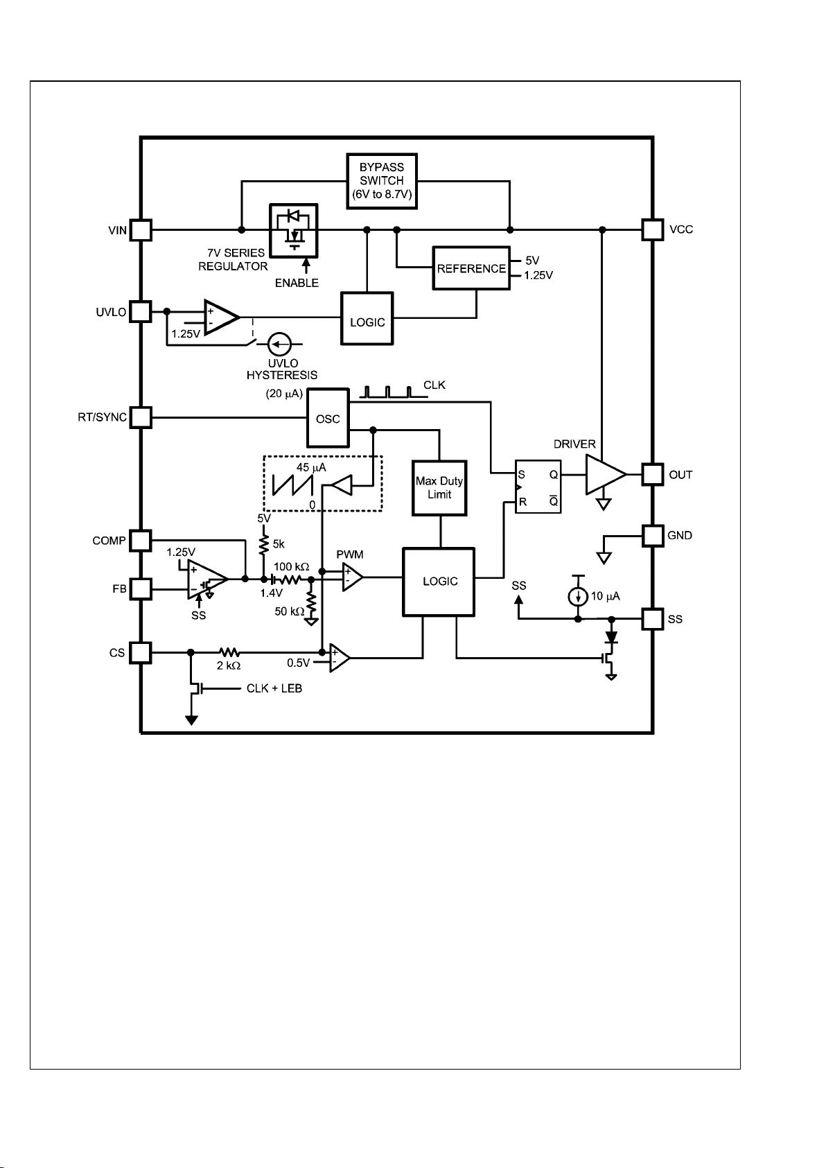
Block Diagram
20212212
7 www.national.com
LM5022
 Loading...