

NSC LM5015MHX, LM5015 Datasheet
December 10, 2007
LM5015
High Voltage Monolithic Two-Switch Forward DC-DC
Regulator
General Description
The LM5015 high voltage switch mode regulator features all
the functions necessary to implement efficient high voltage
Two-Switch Forward and Two-Switch Flyback regulators, using a minimum of external components. This easy to use
regulator integrates high side and low side 75 Volt N-Channel
MOSFETs with a minimum 1 Amp peak current limit. The
voltage across the MOSFETs employed in the two-switch
topology is clamped to the input voltage, allowing the input
voltage range to approach the rating of the MOSFETs. The
regulator control method is based on current mode control
providing inherent ease of loop compensation and line feedforward for superior rejection of input transients.
The operating frequency is set with a single resistor and is
programmable up to 750 kHz. The oscillator can also be synchronized to an external clock. Additional protection features
include cycle-by-cycle current limiting, thermal shutdown, under-voltage lockout and remote shutdown capability. The device is available in the TSSOP-14EP package featuring an
exposed die attach pad to enhance thermal dissipation.
Features
■
Dual Integrated 75V N-Channel MOSFETs
■
Ultra-wide input voltage range: 4.25V to 75V
■
Integrated high voltage bias regulator
■
Adjustable output voltage
■
1.5% feedback reference accuracy
■
Current mode control with selectable compensation
■
Wide bandwidth error amplifier
■
Integrated current sensing and limiting
■
50% maximum duty cycle limit
■
Single resistor oscillator programming
■
Oscillator synchronization capability
■
Programmable soft-start
■
Enable / Under-voltage Lockout (UVLO) pin
■
Thermal shutdown
Package
■
TSSOP-14EP (Exposed Pad)
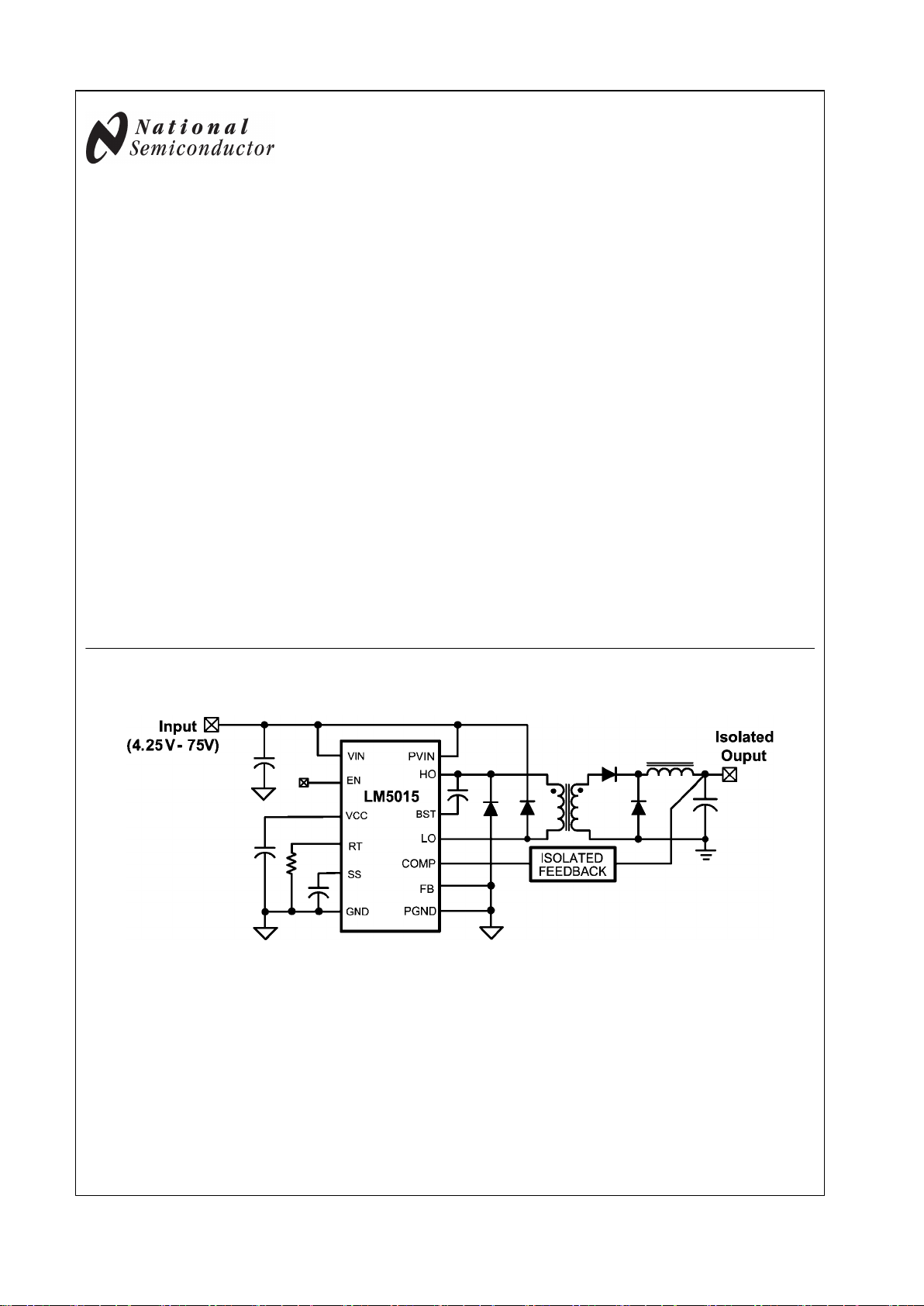
Typical Application Schematic
30034601
© 2007 National Semiconductor Corporation 300346 www.national.com
LM5015 High Voltage Monolithic Two-Switch Forward DC-DC Regulator
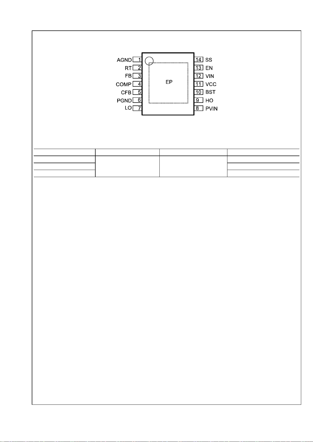
Connection Diagram
30034602
Top View
TSSOP-14 EP Package
Ordering Information
Order Number Package Type NSC Package Drawing Supplied As
LM5015MH
TSSOP-14 EP MXA14A
94 Units per Antistatic Tube
LM5015MHE 250 Units on Tape and Reel
LM5015MHX 2500 Units on Tape and Reel
www.national.com 2
LM5015
Pin Descriptions
Pin Name Description Application Information
1 AGND Analog ground Internal reference for the regulator control functions. The AGND pin and
the PGND pin should be connected directly to minimize switching noise and
prevent erratic operation.
2 RT Oscillator frequency
programming and optional
synchronization input
The internal oscillator is set with a resistor between this pin and the AGND
pin. The recommended switching frequency range is 25KHz to 750 kHz.
The RT pin can accept synchronization pulses from an external clock. A
100 pF capacitor is recommended for coupling the synchronizing clock to
the RT pin.
3 FB Feedback input of the internal
error amplifier, for non-isolated
applications
This pin is connected to the inverting input of the internal error amplifier.
The 1.26V reference is internally connected to the non-inverting input of
the error amplifier. In isolated application using an external error amplifier,
this pin should be connected to the AGND pin.
4 COMP Control input for the PWM
comparator
Internally connected to the open drain output of the internal error amplifier.
COMP pull-up is provided by an internal 5 kΩ resistor which may be used
to bias an opto-coupler transistor in isolated applications.
5 CFB Current feedback pin Feedback in put for high bandwidth isolated applications. An NPN current
mirror couples the external opto-coupler current to the PWM comparator
while maintaining a relatively constant opto-coupler voltage.
6 PGND Power ground Internally connected to the current sense resistor in the source of the low
side MOSFET switch.
7 LO Low side switch drain The drain terminal of the internal low side power MOSFET.
8 PVIN Input supply pin for high side
switch
Internally connected to the drain of the high side power MOSFET.
9 HO High side switch source The source terminal of the high side power MOSFET.
10 BST High side bootstrap bias An external capacitor is required between the BST and the HO pins. A
minimum capacitor value of 0.022 µF is recommended. The capacitor is
charged from VCC via an internal diode during the power MOSFET off-time.
11 VCC Bias regulator output, or input for
external bias supply
VCC tracks VIN up to 6.9V. At higher VIN voltages, VCC is regulated to 6.9
Volts. A 0.47µF or greater ceramic decoupling capacitor is required on the
VCC pin. An external bias voltage between 7V and 14V applied to the VCC
pin will disable the internal VCC regulator, reduce internal power
dissipation, and improve the converter efficiency.
12 VIN Analog input voltage pin Power supply Input for the switching regulator control blocks.
13 EN Enable / Under-Voltage Lock-
Out / Shutdown input
An external voltage divider can be used to set the input under-voltage
lockout threshold. If the EN pin is left unconnected, a 6 µA pull-up current
source pulls the EN pin high to enable the regulator.
14 SS Soft-start An internal 11 µA current source charges an external capacitor connected
to the SS pin to soft-start the switching regulator by gradually raising the
COMP pin voltage.
NA EP Exposed Pad Exposed metal pad on the underside of the package. It is recommended to
connect this pad to the PGND and AGND pins, and also to the PC board
ground plane in order to improve heat dissipation.
3 www.national.com
LM5015
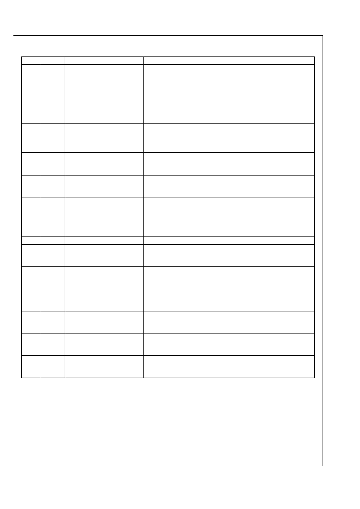
Absolute Maximum Ratings (Note 1)
If Military/Aerospace specified devices are required,
please contact the National Semiconductor Sales Office/
Distributors for availability and specifications.
VIN to AGND 76V
BST to AGND 90V
PVIN to HO, LO, PGND 76V
HO to PGND (Steady State) -3V to 76V
LO to PGND (Steady State) -0.3V to 76V
BST to VCC 76V
BST to HO 14V
VCC, EN to AGND 14V
COMP, FB, RT, SS to AGND -0.3V to 7V
PGND to AGND -0.3V to +0.3V
CFB Sink Current 10 mA
Maximum Junction Temperature 150°C
Storage Temperature −65°C to + 150°C
ESD Rating
Human Body Model 2 kV
Operating Ratings
V
IN
4.25V to 75V
Operation Junction Temperature −40°C to + 125°C
Electrical Characteristics Limits in standard type are for T
J
= 25°C only; limits in boldface type apply over the
junction temperature (TJ) range of −40°C to + 125°C. Minimum and Maximum limits are guaranteed through test, design, or
statistical correlation. Typical values represent the most likely parametric norm at TJ = 25°C, and are provided for reference
purposes only. V
VIN
= 48V, RRT = 31.6 kΩ unless otherwise stated. See (Note 3).
Symbol Parameters Conditions Min Typ Max Units
STARTUP REGULATOR
V
VCC-REG
VCC Regulator Output 6.35 6.85 7.25 V
VCC Current Limit V
VCC
= 6V 20 25 mA
VCC UVLO Threshold VCC increasing, VIN = VCC, EN=open 3.45 3.75 4.05 V
VCC UVLO Hysteresis VIN = VCC, EN = open 0.15 V
Bias Current (IIN) VFB = 1.5V 3.1 4.5 mA
I
Q
Shutdown Current (IIN) VEN = 0V 110 170 µA
EN THRESHOLDS
EN Shutdown Threshold VEN increasing 0.25 0.45 0.65 V
EN Shutdown Hysteresis 0.1 V
EN Standby Threshold VEN increasing 1.19 1.26 1.3 V
EN Standby Hysteresis 0.1 V
EN Current Source 6 µA
MOSFET CHARACTERSTICS
Low side MOSFET RDS(ON) plus
Current Sense Resistance
ID = 0.6A 0.49 0.93
Ω
MOSFET Leakage Current VLO = 75V 0.05 5 µA
High side MOSFET RDS(ON) ID = 0.6A 0.45 0.90
Ω
MOSFET Leakage Current V
PVIN
= 75V, VHO = PGND 0.05 5 µA
Total Gate Charge including both
Low and High side MOSFETs
V
VCC
= 8V 9 nC
Pre-charge Switch ON Voltage
including series blocking diode
ID = 1 mA 0.82 V
CURRENT LIMIT
I
LIM
Cycle by Cycle Current Limit 1 1.2 1.4 A
Cycle by Cycle Current Limit
Delay
130 ns
OSCILLATOR
F
SW1
Frequency1 RRT = 31.6k 180 200 220 kHz
F
SW2
Frequency2 RRT = 15.4k 365 405 445 kHz
V
RT-SYNC
SYNC Threshold VRT Increasing 3.2 V
SYNC Pulse Width Minimum VRT > V
RT-SYNC
+ 0.5V 15 ns
www.national.com 4
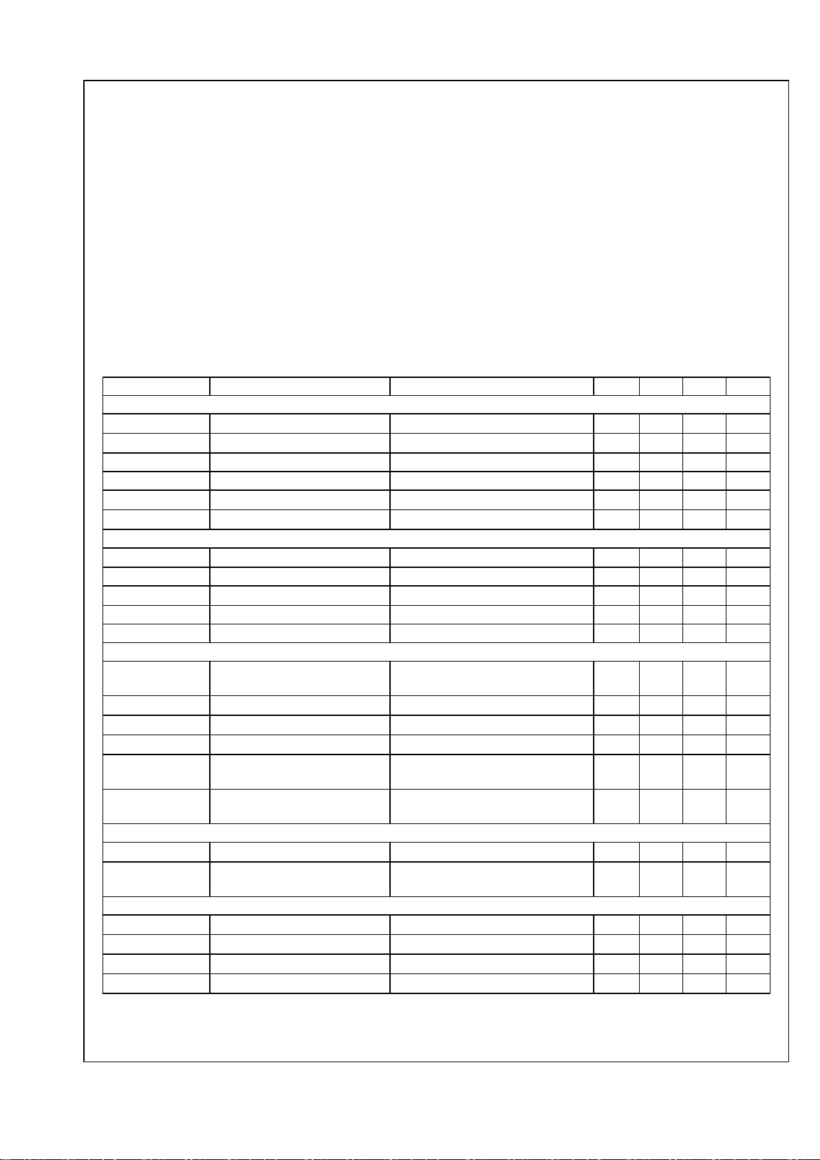
LM5015
Symbol Parameters Conditions Min Typ Max Units
PWM COMPARATOR
Maximum Duty Cycle 49 %
Min On-time V
COMP
> V
COMP-OS
140 ns
Min On-time V
COMP
< V
COMP-OS
0 ns
V
COMP-OS
COMP to PWM Comparator
Offset
0.9 1.3 1.55 V
ERROR AMPLIFIER
V
FB-REF
Feedback Reference Voltage Internal reference, VFB = V
COMP
1.236 1.26 1.274 V
FB Bias Current 10 nA
DC Gain 72 dB
COMP Sink Current V
COMP
= 250mV 2 mA
COMP Short Circuit Current VFB = 0, V
COMP
= 0 0.9 1.2 1.5 mA
COMP Open Circuit Voltage VFB = 0 4.5 5.15 5.95 V
COMP to SW Delay 50 ns
Unity Gain Bandwidth 4 MHz
SOFT START
Soft-start Current Source 8 11 14 µA
Soft-start to COMP Offset 0.3 0.5 0.7 V
THERMAL SHUTDOWN
T
SD
Thermal Shutdown Threshold 165 °C
Thermal Shutdown Hysteresis 25 °C
THERMAL RESISTANCE
θ
JC
Junction to Case 6.6 °C/W
θ
JA
Junction to Ambient 40 °C/W
Note 1: Absolute Maximum Ratings are limits beyond which damage to the device may occur. Operating Ratings are conditions under which operation of the
device is intended to be functional. For guaranteed specifications and test conditions, see the Electrical Characteristics.
Note 2: The human body model is a 100pF capacitor discharged through a 1.5 kΩ resistor into each pin. Test Method is per JESD-22-A114.
Note 3: Min and Max limits are 100% production tested at 25°C. Limits over the operating temperature range are guaranteed through correlation using Statistical
Quality Control (SQC) methods. Limits are used to calculate National’s Average Outgoing Quality Level (AOQL).
5 www.national.com
LM5015
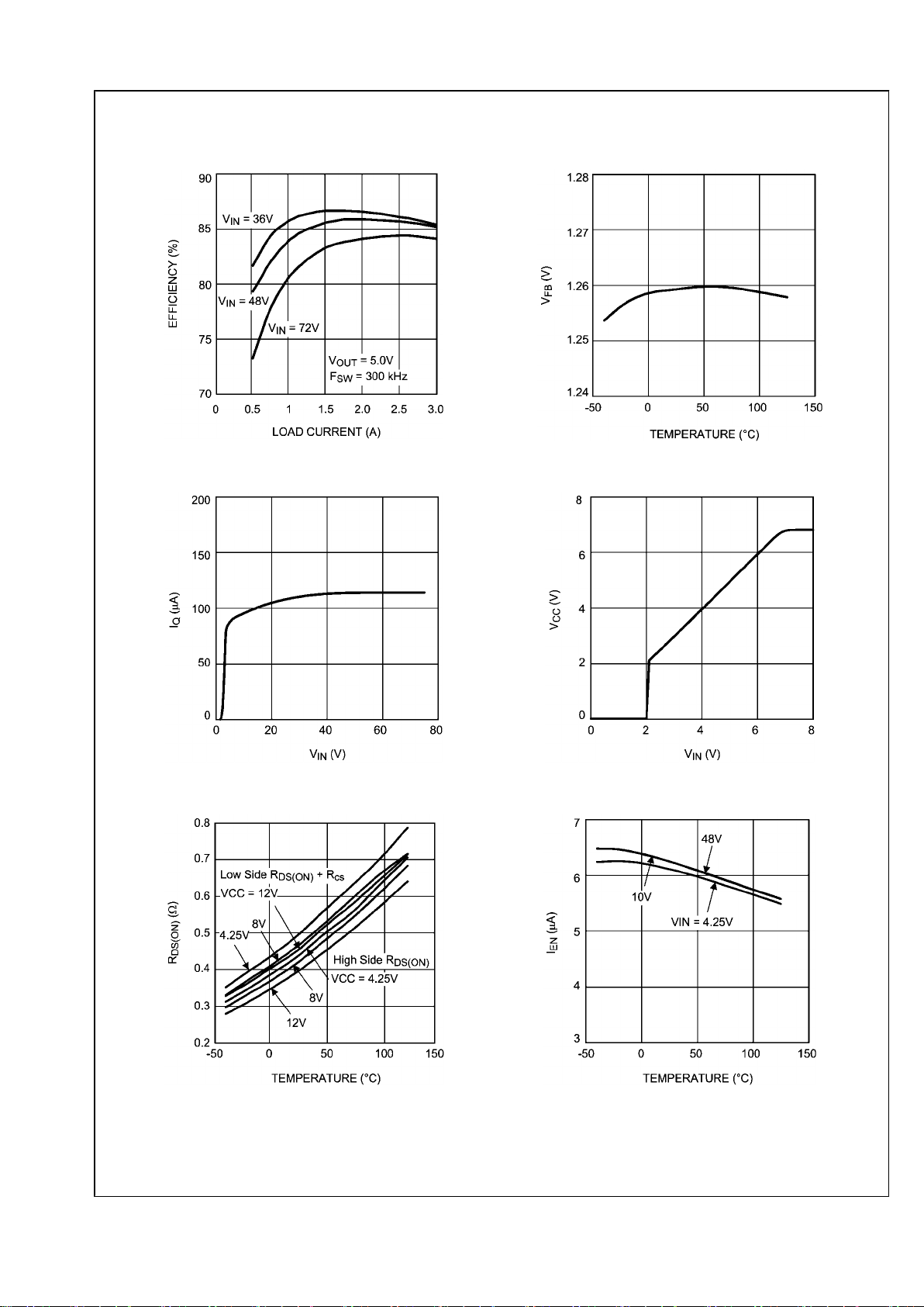
Typical Performance Characteristics
Demo-board Efficiency vs I
OUT
and V
IN
30034603
VFB vs Temperature
30034604
IQ (non-switching) vs VIN
30034605
VCC vs VIN
30034606
RDS(ON) vs VCC vs Temperature
30034607
IEN vs VIN vs Temperature
30034608
www.national.com 6
LM5015
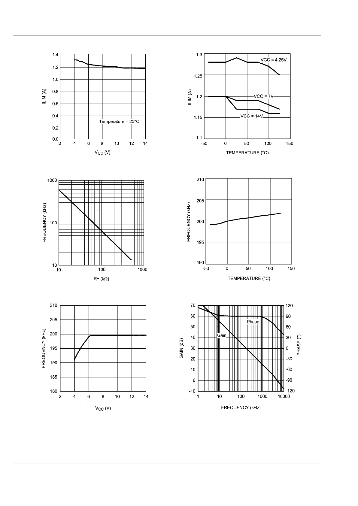
ILIM vs VCC
30034609
ILIM vs VCC vs Temperature
30034610
Fsw vs R
RT
30034611
Fsw vs Temperature
30034612
Fsw vs VCC
30034613
Error Amplifier Gain/Phase
30034614
7 www.national.com
LM5015
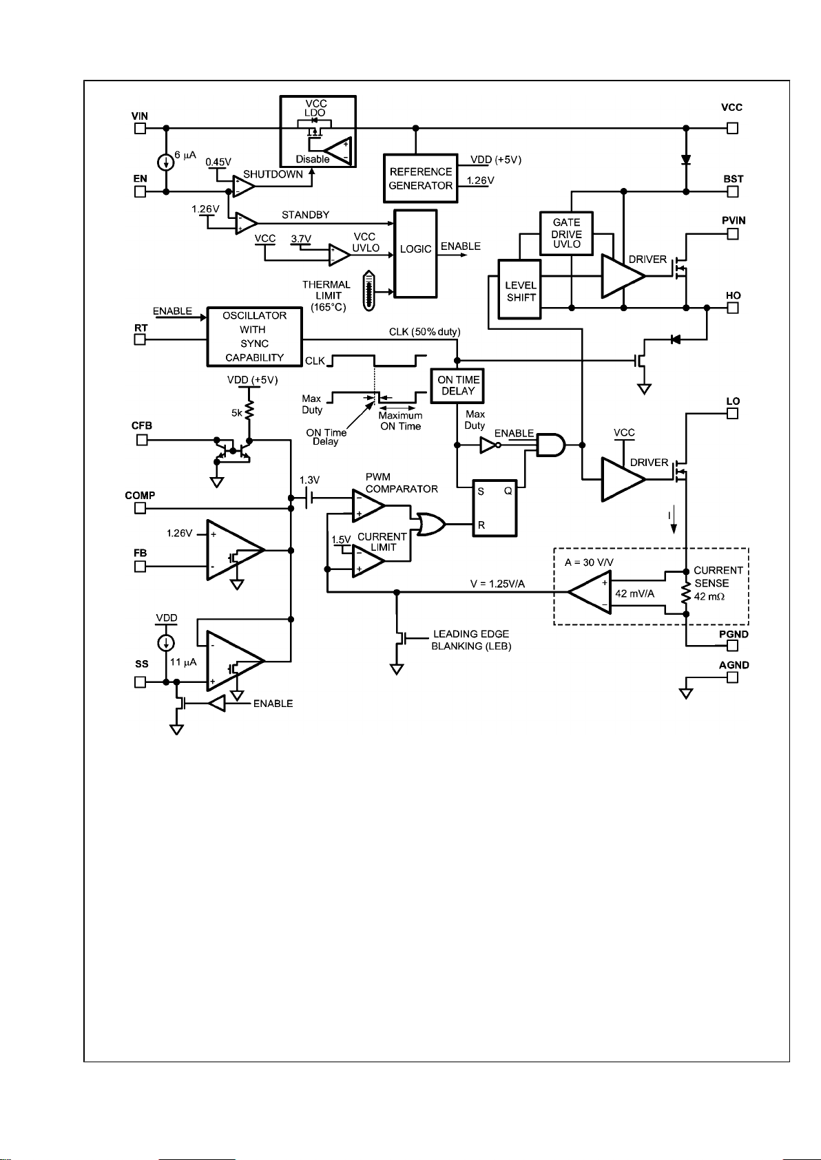
30034615
FIGURE 1. Block Diagram
www.national.com 8
LM5015
 Loading...