

LM5000
High Voltage Switch Mode Regulator
General Description
The LM5000 is a monolithic integrated circuit specifically
designed and optimized for flyback, boost or forward power
converter applications. The internal power switch is rated for
a maximum of 80V, with a current limit set to 2A. Protecting
the power switch are current limit and thermal shutdown
circuits. The current mode control scheme provides excellent
rejection of line transients and cycle-by-cycle current limiting.
An external compensation pin and the built-in slope compensation allow the user to optimize the frequency compensation. Other distinctive features include softstart to reduce
stresses during start-up and an external shutdown pin for
remote ON/OFF control. There are two operating frequency
ranges available. The LM5000-3 is pin selectable for either
300kHz (FS Grounded) or 700kHz (FS Open). The
LM5000-6 is pin selectable for either 600kHz (FS Grounded)
or 1.25MHz (FS Open). The device is available in a low
profile 16-lead TSSOP package (available now) or a thermally enhanced 16-lead LLP package (coming in Q3CY03).
Features
n 80V internal switch
n Operating input voltage range of 3.1V to 40V
n Pin selectable operating frequency
300kHz/700kHz (-3)
600kHz/1.25MHz (-6)
n Adjustable output voltage
n External compensation
n Input undervoltage lockout
n Softstart
n Current limit
n Over temperature protection
n External shutdown
n Small 16-Lead TSSOP or 16-Lead LLP package
Applications
n Flyback Regulator
n Forward Regulator
n Boost Regulator
n DSL Modems
n Distributed Power Converters
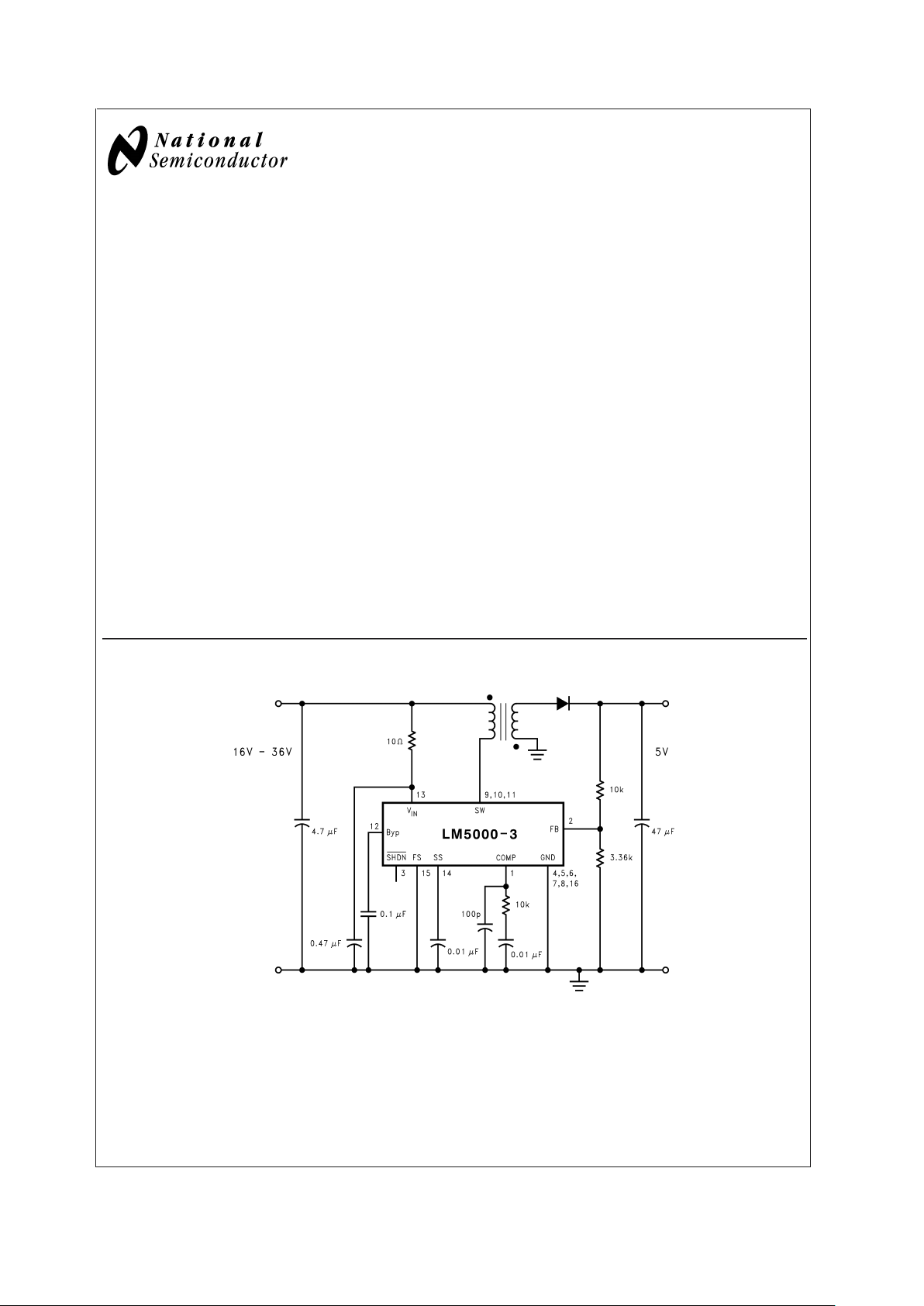
Typical Application Circuit
20031901
LM5000 Flyback Converter
July 2003
LM5000 High Voltage Switch Mode Regulator
© 2003 National Semiconductor Corporation DS200319 www.national.com
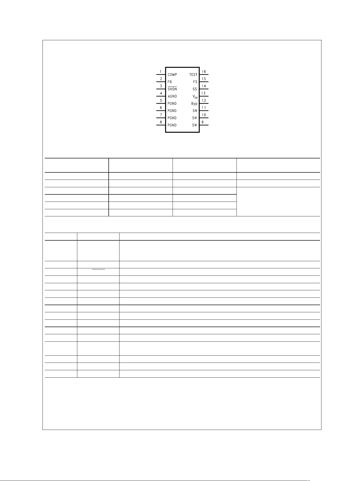
Connection Diagram
Top View
20031904
Ordering Information
Order Number Package Type NSC Package
Drawing
Supplied As
LM5000-3MTC TSSOP-16 MTC16 94 Units, Rail
LM5000-3MTCX TSSOP-16 MTC16 2500 Units, Tape and Reel
LM5000SD-3 LLP-16 SDA16
Coming in Q3CY03
LM5000SDX-3 LLP-16 SDA16
LM5000SD-6 LLP-16 SDA16
LM5000SDX-6 LLP-16 SDA16
Pin Description
Pin Name Function
1 COMP Compensation network connection. Connected to the output of the voltage error amplifier.
The RC compenstion network should be connected from this pin to AGND. An additional
100pF high frequency capacitor to AGND is recommended.
2 FB Output voltage feedback input.
3 SHDN
Shutdown control input, Open = enable, Ground = disable.
4 AGND Analog ground, connect directly to PGND.
5 PGND Power ground.
6 PGND Power ground.
7 PGND Power ground.
8 PGND Power ground.
9 SW Power switch input. Switch connected between SW pins and PGND pins
10 SW Power switch input. Switch connected between SW pins and PGND pins
11 SW Power switch input. Switch connected between SW pins and PGND pins
12 BYP Bypass-Decouple Capacitor Connection, 0.1µF ceramic capacitor recommended.
13 V
IN
Analog power input. A small RC filter is recommended, to suppress line glitches. Typical
values of 10Ω and ≥ 0.1µF are recommended.
14 SS Softstart Input. External capacitor and internal current source sets the softstart time.
15 FS Switching frequency select input. Open = F
high
. Ground = F
low
16 TEST Factory test pin, connect to ground.
LM5000
www.national.com 2
Absolute Maximum Ratings (Note 1)
If Military/Aerospace specified devices are required,
please contact the National Semiconductor Sales Office/
Distributors for availability and specifications.
V
IN
-0.3V to 40V
SW Voltage -0.3V to 80V
FB Voltage -0.3V to 5V
COMP Voltage -0.3V to 3V
All Other Pins -0.3V to 7V
Maximum Junction Temperature 150˚C
Power Dissipation(Note 2) Internally Limited
Lead Temperature 216˚C
Infrared (15 sec.) 235˚C
ESD Susceptibility (Note 3)
Human Body Model 2kV
Machine Model 200V
Storage Temperature −65˚C to +150˚C
Operating Conditions
Operating Junction
Temperature Range
(Note 7) −40˚C to +125˚C
Supply Voltage (Note 7) 3.1V to 40V
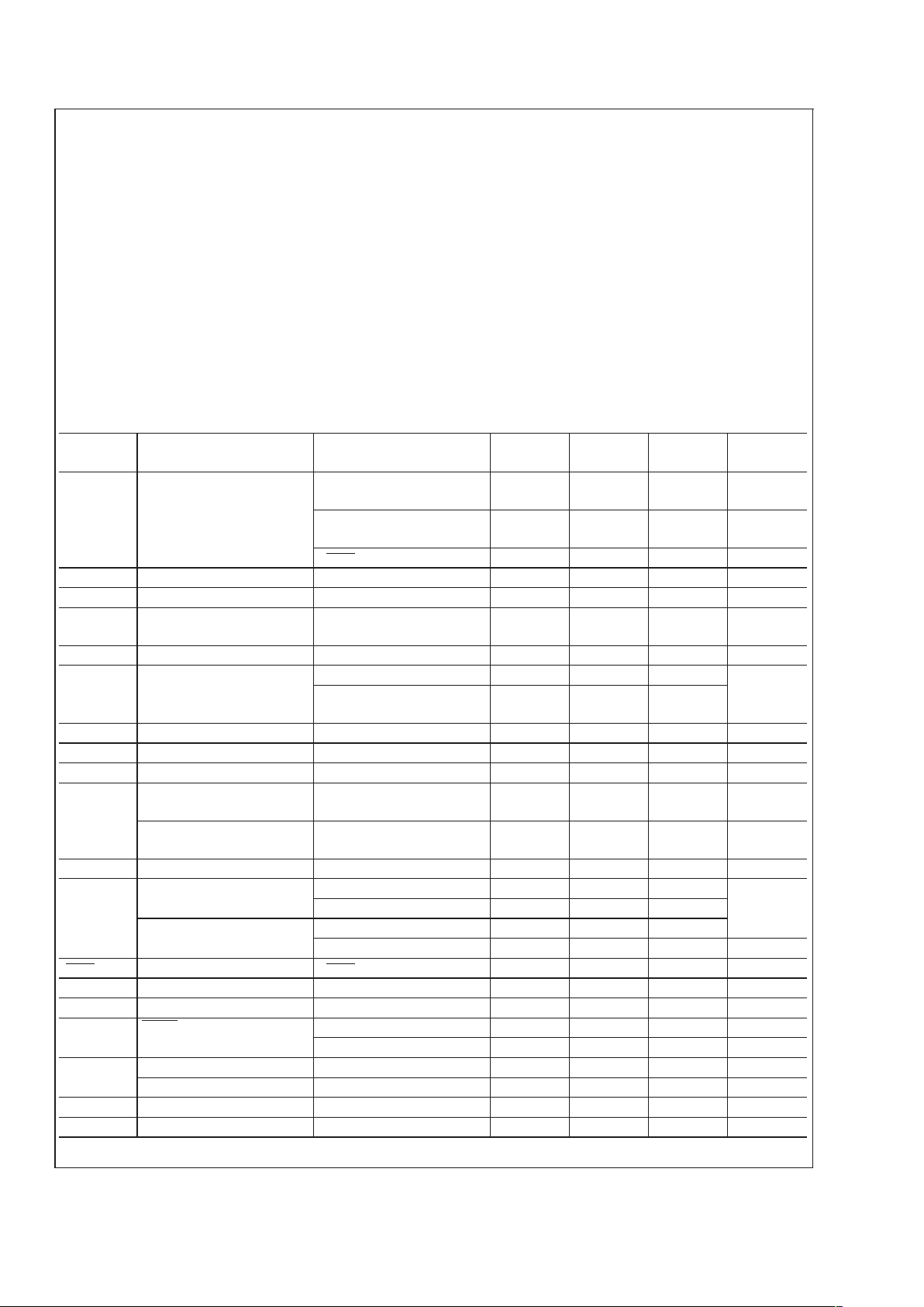
Electrical Characteristics
Specifications in standard type face are for TJ= 25˚C and those with boldface type apply over the full Operating Temperature Range (T
J
= −40˚C to +125˚C) Unless otherwise specified. VIN= 12V and IL= 0A, unless otherwise specified.
Symbol Parameter Conditions
Min
(Note 4)
Typ
(Note 5)
Max
(Note 4)
Units
I
Q
Quiescent Current FB = 2V (Not Switching)
FS=0V
2.0 2.5 mA
FB = 2V (Not Switching)
FS = Open
2.1 2.5 mA
V
SHDN
=0V 18 30 µA
V
FB
Feedback Voltage 1.2330 1.259 1.2840 V
I
CL
Switch Current Limit 1.35 2.0 2.7 A
%V
FB
/∆VINFeedback Voltage Line
Regulation
3.1V ≤ VIN≤ 40V 0.001 0.04 %/V
I
B
FB Pin Bias Current (Note 6) 55 200 nA
BV Output Switch Breakdown
Voltage
T
J
= 25˚C, ISW= 0.1µA 80 V
T
J
= -40˚C to + 125˚C, ISW=
0.5µA
76
V
IN
Input Voltage Range 3.1 40 V
g
m
Error Amp Transconductance ∆I = 5µA 150 410 750 µmho
A
V
Error Amp Voltage Gain 280 V/V
D
MAX
Maximum Duty Cycle
LM5000-3
FS=0V 85 90 %
Maximum Duty Cycle
LM5000-6
FS = 0V TBD 90 %
T
MIN
Minimum On Time 165 ns
f
S
Switching Frequency
LM5000-3
FS=0V 240 300 360
kHz
FS = Open 550 700 840
Switching Frequency
LM5000-6
FS=0V TBD 600 TBD
FS = Open TBD 1.25 TBD MHz
I
SHDN
Shutdown Pin Current V
SHDN
=0V −1 -2 µA
I
L
Switch Leakage Current VSW= 80V 0.008 5 µA
R
DSON
Switch R
DSON
ISW= 1A 160 445 mΩ
Th
SHDN
SHDN Threshold Output High 0.9 0.6 V
Output Low 0.6 0.3 V
UVLO On Threshold 2.74 2.92 3.10 V
Off Threshold 2.60 2. 77 2.96 V
OVP V
COMP
Trip 0.67 V
I
SS
Softstart Current 8 11 14 µA
LM5000
www.national.com3
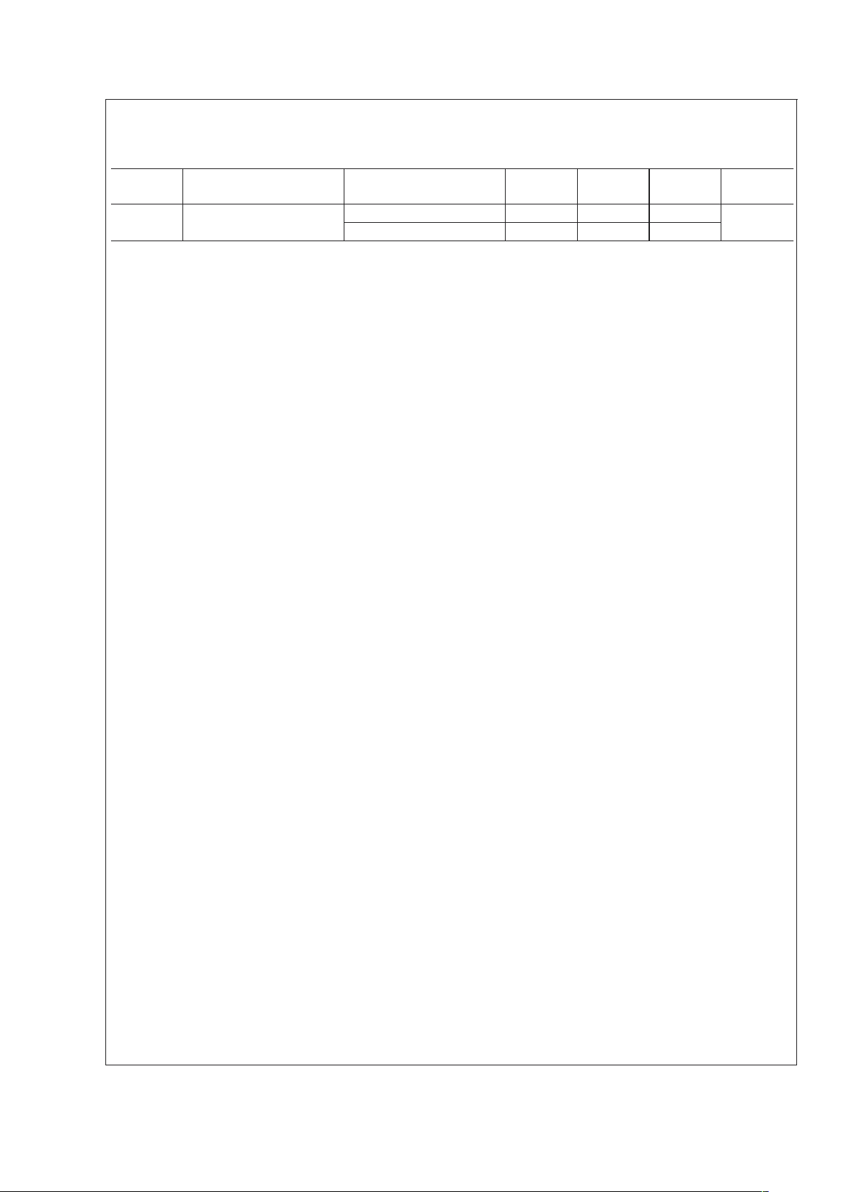
Electrical Characteristics (Continued)
Specifications in standard type face are for TJ= 25˚C and those with boldface type apply over the full Operating Temperature Range (T
J
= −40˚C to +125˚C) Unless otherwise specified. VIN= 12V and IL= 0A, unless otherwise specified.
Symbol Parameter Conditions
Min
(Note 4)
Typ
(Note 5)
Max
(Note 4)
Units
θ
JA
Thermal Resistance TSSOP, Package only 150 ˚C/W
LLP, Package only 45
Note 1: Absolute maximum ratings are limits beyond which damage to the device may occur. Operating Ratings are conditions for which the device is intended to
be functional, but device parameter specifications may not be guaranteed. For guaranteed specifications and test conditions, see the Electrical Characteristics.
Note 2: The maximum allowable power dissipation is a function of the maximum junction temperature, T
J
(MAX), the junction-to-ambient thermal resistance, θJA,
and the ambient temperature, T
A
. See the Electrical Characteristics table for the thermal resistance of various layouts. The maximum allowable power dissipation
at any ambient temperature is calculated using: P
D
(MAX) = (T
J(MAX)−TA
)/θJA. Exceeding the maximum allowable power dissipation will cause excessive die
temperature, and the regulator will go into thermal shutdown.
Note 3: The human body model is a 100 pF capacitor discharged through a 1.5kΩ resistor into each pin. The machine model is a 200pF capacitor discharged
directly into each pin.
Note 4: All limits guaranteed at room temperature (standard typeface) and at temperature extremes (bold typeface). All room temperature limits are 100%
production tested. All limits at temperature extremes are guaranteed via correlation using standard Statistical Quality Control (SQC) methods. All limits are used to
calculate Average Outgoing Quality Level (AOQL).
Note 5: Typical numbers are at 25˚C and represent the most likely norm.
Note 6: Bias current flows into FB pin.
Note 7: Supply voltage, bias current product will result in aditional device power dissipation. This power may be significant. The thermal dissipation design should
take this into account.
LM5000
www.national.com 4
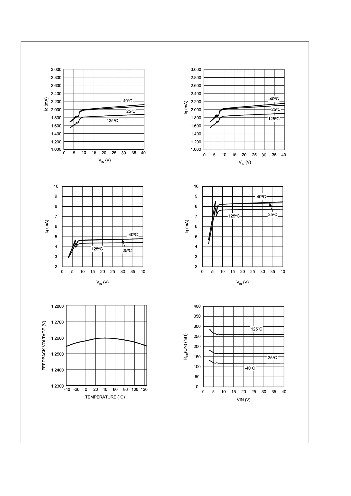
Typical Performance Characteristics
Iq (non-switching) vs V
IN
@
fSW= 300kHz Iq (non-switching) vs V
IN
@
fSW= 700kHz
20031920
20031921
Iq (switching) vs V
IN
@
fSW= 300kHz Iq (switching) vs V
IN
@
fSW= 700kHz
20031922 20031923
Vfbvs Temperature R
DS(ON)
vs V
IN
@
ISW=1A
20031924
20031925
LM5000
www.national.com5
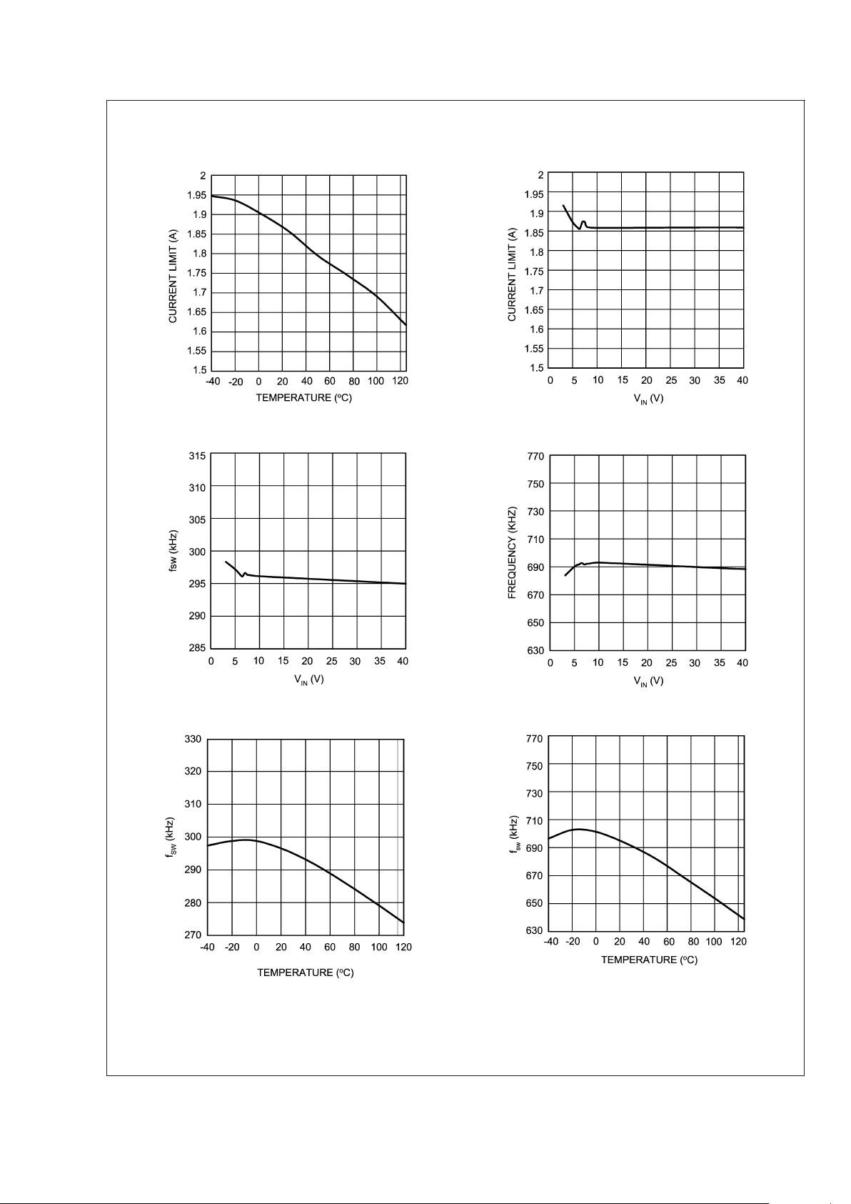
Typical Performance Characteristics (Continued)
Current Limit vs Temperature Current Limit vs V
IN
20031926
20031927
fSWvs. V
IN
@
FS = Low (-3) fSWvs. V
IN
@
FS = High (-3)
20031928
20031929
fSWvs. Temperature@FS = Low (-3) fSWvs. Temperature@FS = High (-3)
20031930
20031931
LM5000
www.national.com 6
 Loading...