

NSC LM494IN, LM494CN, LM494CJ Datasheet
TL/H/10056
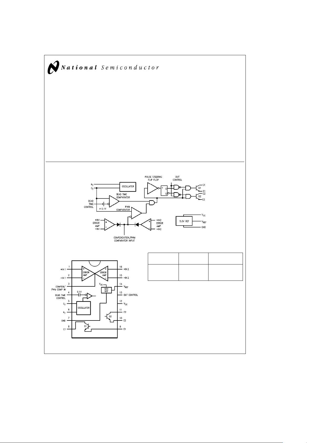
LM494 Pulse Width Modulated Control Circuit
June 1989
LM494
Pulse Width Modulated Control Circuit
General Description
The LM494 is a monolithic integrated circuit which includes
all the necessary building blocks for the design of pulse
width modulated (PWM) switching power supplies, including
push-pull, bridge and series configurations. The device can
operate at switching frequencies between 1.0 kHz and
300 kHz and output voltages up to 40V. The operating temperature range specified for the LM494C is 0
§
Cto70§C and
for the LM494V is
b
40§Ctoa85§C.
Features
Y
Uncommitted output transistors capable of 200 mA
source or sink
Y
On-chip error amplifiers
Y
On-chip 5.0V reference
Y
Internal protection from double pulsing of outputs with
narrow pulse widths or with supply voltages below
specified limits
Y
Dead time control comparator
Y
Output control selects single ended or push-pull operation
Y
Easily synchronized (slaved) to other circuits
Block Diagram
TL/H/10056– 2
Connection Diagram
16-Lead DIP
TL/H/10056– 1
Top View
Ordering Information
Device Package Package
Code Code Description
LM494IN N16A Molded DIP
LM494CJ J16A Ceramic DIP
LM494CN N16A Molded DIP
C
1995 National Semiconductor Corporation RRD-B30M115/Printed in U. S. A.
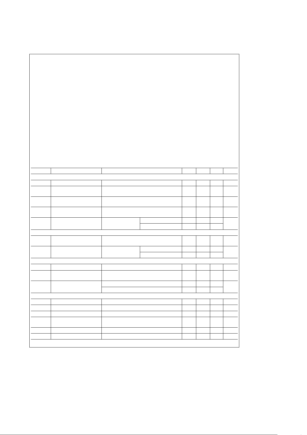
Absolute Maximum Ratings
If Military/Aerospace specified devices are required,
please contact the National Semiconductor Sales
Office/Distributors for availability and specifications.
Storage Temperature Range
Ceramic DIP
b
65§Ctoa175§C
Molded DIP
b
65§Ctoa150§C
Operating Temperature Range
Industrial (LM494I)
b
40§Ctoa85§C
Commercial (LM494C) 0
§
Ctoa70§C
Lead Temperature
Ceramic DIP (Soldering, 60 sec.) 300
§
C
Molded DIP (Soldering, 10 sec.) 265
§
C
Internal Power Dissipation (Notes 1, 2)
16L-Ceramic DIP 1.50W
16L-Molded DIP 1.04W
Supply Voltage 42V
Voltage from Any Lead to Ground
(except Lead 8 and Lead 11) V
CC
a
0.3V
Output Collector Voltage 42V
Peak Collector Current
(I
C1
and IC2) 250 mA
ESD Susceptibility (to be determined)
Recommended Operating
Conditions
Power Supply Voltage (VCC) 7.0V to 40V
Voltage on Any Lead
except Leads 8 and 11
(Referenced to Ground) (V
I
)
b
0.3V to V
CC
a
0.3V
Output Voltage Collector (V
C1,VC2
)
b
0.3V to 40V
Output Collector Current (IC1,IC2) 200 mA
Timing Capacitor (CT) 470 pF to 10 mF
Timing Resistor (RT) 1.8 kX to 500 kX
Oscillator Frequency (f
OSC
) 1.0 kHz to 300 kHz
LM494
Electrical Characteristics
T
A
e
0§Ctoa70§C for the LM494C, T
A
eb
40§Ctoa85§C for the LM494I, V
CC
e
15V, f
OSC
e
10 kHz, unless otherwise specified
Symbol Parameter Conditions Min Typ Max Units
REFERENCE SECTION
V
REF
Reference Voltage (Note 3) I
REF
e
1.0 mA 4.75 5.0 5.25 V
Reg
LINE
Line Regulation of 7.0VsV
CC
s
40V
2.0 25 mV
Reference Voltage
TCV
REF
Temperature Coefficient of 0§CsT
A
s
70§C
0.01 0.03 %/
§
C
Reference Voltage
Reg
LOAD
Load Regulation of 1.0 mAsI
REF
s
10 mA
1.0 15 mV
Reference Voltage
I
OS
Output Short Circuit Current V
REF
e
0V 0§CsT
A
s
a
70§C103550
mA
b
40§CsT
A
s
a
85§C35
OSCILLATOR SECTION
f
OSC
Oscillator Frequency C
T
e
0.01 mF,
10 kHz
(Figure 10)
R
T
e
12 kX
Df
OSC
Oscillator Frequency Change C
T
e
0.01 mF, 0§CsT
A
s
a
70§C 2.0
%
R
T
e
12 kX
b
40§CsT
A
s
a
85§C 2.0
DEAD TIME CONTROL SECTION
I
IB (DT)
Input Bias Current V
CC
e
15V, 0VsV
4
s
5.25V
b
2.0b10 mA
DC
(Max)
Maximum Duty Cycle, V
CC
e
15V, Lead 4e0V,
45 %
Each Output Output Control
e
V
REF
V
TH(in)
Input Threshold Voltage Zero Duty Cycle 3.0 3.3
V
Maximum Duty Cycle 0
ERROR AMPLIFIER SECTIONS
V
IO
Input Offset Voltage V
3
e
2.5VV
3
e
2.5V 2.0 10 mV
I
IO
Input Offset Current V
3
e
2.5V 25 250 nA
I
IB
Input Bias Current V
3
e
2.5V 0.2 1.0 mA
V
ICR
Input Common Mode 7.0VsV
CC
s
40V
b
0.3 V
CC
V
Voltage Range
A
VS
Large Signal Voltage Gain 0.5VsV
3
s
3.5V 60 74 dB
BW Bandwidth 650 kHz
2
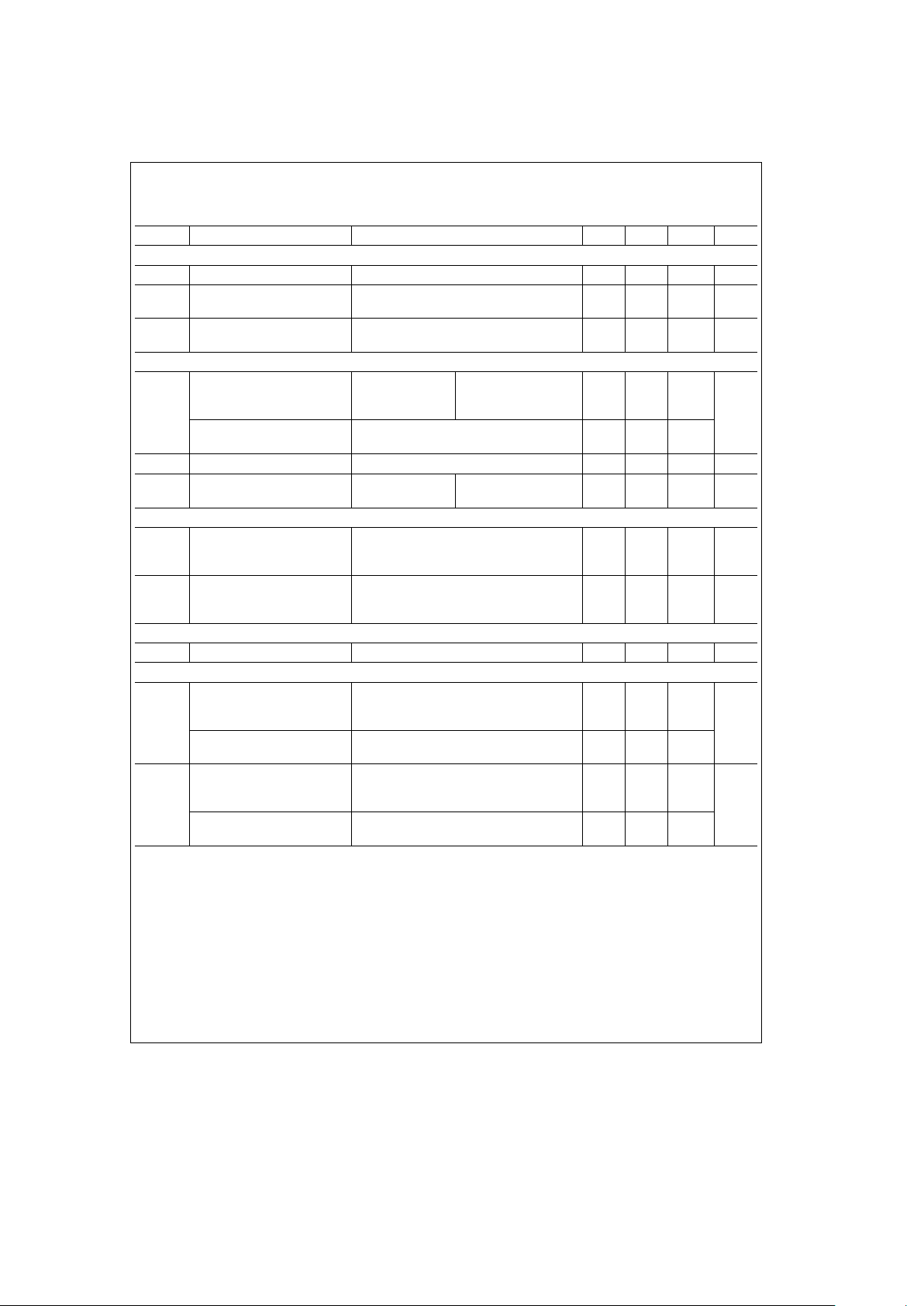
LM494
Electrical Characteristics
T
A
e
0§Ctoa70§C for the LM494C, T
A
eb
40§Ctoa85§C for the LM494I,
V
CC
e
15V, f
OSC
e
10 kHz, unless otherwise specified (Continued)
Symbol Parameter Conditions Min Typ Max Units
PWM COMPARATOR SECTION
(Figure 9)
V
THI
Inhibit Threshold Voltage Zero Duty Cycle 4.0 4.5 V
I
O
b
Output Sink Current 0.5VsV
3
s
3.5V
b
0.2b0.6 mA
(Note 4)
I
O
a
Output Source Current 0.5VsV
3
s
3.5V
2.0 mA
(Note 4)
OUTPUT SECTION
V
CE(sat)
Output Saturation V
E
e
0V, 0§CsT
A
s
a
70§C
Voltage Common Emitter I
C
e
200 mA
b
40§CsT
A
s
a
85§C 1.1 1.3
Configuration
(Figure 3)
V
Emitter Follower V
C
e
15V, I
E
e
200 mA
1.5 2.5
Configuration
(Figure 4)
I
C(off)
Collector Off-State Current V
CC
e
40V, V
CE
e
40V 2.0 100 mA
I
E(off)
Emitter Off-State Current V
CC
e
V
C
e
40V, 0§CsT
A
s
a
70§C,
b
100 mA
V
E
e
0
b
40§CsT
A
s
a
85§C
OUTPUT CONTROL
(Figure 6)
V
OCL
Output Control Voltage
Required for Single Ended or 0.4 V
Parallel Output Operation
V
OCH
Output Control Voltage
Required for Push-Pull 2.4 V
Operation
TOTAL DEVICE
I
CC
Standby Power Supply Current 6.0 10 mA
OUTPUT AC CHARACTERISTICS Use Recommended Operating Conditions with T
A
e
25§C
t
r
Rise Time of Output Voltage
Common Emitter Configuration 100 200
(Figure 3)
ns
Emitter Follower Configuration
100 200
(Figure 4)
t
f
Fall Time of Output Voltage
Common Emitter Configuration 25 100
(Figure 3)
ns
Emitter Follower Configuration
40 100
(Figure 4)
Note 1: T
J Max
e
150§C for the Molded DIP, and 175§C for the Ceramic DIP.
Note 2: Ratings apply to ambient temperature at 25
§
C. Above this temperature, derate the 16L-Ceramic DIP at 10 mW/§C, and the 16L-Molded DIP at 8.3 mW/§C.
Note 3: Selected devices with tightened tolerance reference voltage available.
Note 4: These limits apply when the voltage measured at Lead 3 is within the range specified.
3
 Loading...