

NSC LM4930ITL, LM4930ITLX Datasheet
LM4930
Audio Subsystem with Stereo Headphone & Mono
Speaker Amplifiers
General Description
The LM4930 is an integrated audio subsystem that supports
voice and digital audio functions. The LM4930 includes a
high quality I
2
S input stereo DAC, a voice band codec, a
stereo headphone amplifier and a high-power mono speaker
amplifier. It is primarily designed for demanding applications
in mobile phones and other portable devices.
The LM4930 features an I
2
S serial interface for full range
audio, a 16-bit PCM bi-directional serial interface for the
voice band codec and an two-wire interface for control. The
full range music path features an SNR of 86dB with a 16-bit
48kHz input. The stereo DAC can also be used while the
voice codec is in use. The headphone amplifier delivers
25mW
RMS
toa32Ω single-ended stereo load with less than
0.5% distortion (THD+N) when AV
DD
= 3V. The mono
speaker amplifier delivers up to 300mW into an 8Ω load with
less than 2% distortion when AV
DD
=3V.
The LM4930 employs advanced techniques to reduce power
consumption, to reduce controller overhead and to eliminate
click and pop. Boomer audio power amplifiers were designed specifically to provide high quality output power with
a minimal amount of external components. It is, therefore,
ideally suited for mobile phone and other low voltage applications where minimal power consumption is a primary requirement.
Key Specifications
j
P
H/P OUT
at AVDD= 3.0V, 32Ω
0.5% THD+N 25mW (typ)
j
P
LS OUT
at AVDD= 3.0V, 8Ω
2% THD+N 300mW (typ)
j
Supply voltage range
DV
DD
(Note 8) 2.6V to 4.5V
AV
DD
(Note 8) 2.6V to 5.5V
j
Total shutdown current 2µA (typ)
j
PSRR at 217Hz, AVDD= 3V 50dB (typ)
Features
n 16-bit resolution 48kHz stereo DAC
n 16-bit resolution 8kHz voice codec
n I
2
S digital audio data serial interface
n Two-wire serial control interface
n PCM voice audio data serial interface
n 25mW/channel stereo headphone amplifier
n 300mW mono 8Ω amplifier (at AV
DD
= 3.0V)
n 32-step volume control for audio output amplifiers
n No snubber networks or bootstrap capacitors are
required by the headphone or hands-free amplifiers
n Digital sidetone generation with adjustable attenuation
n Gain controllable headphone amp, mono BTL amp, mic
preamp
n Available in the 36 bump micro SMD package
Applications
n Mobile Phones
n Mobile/low power audio appliances
n PDAs
Boomer®is a registered trademark of National Semiconductor Corporation.
July 2003
LM4930 Audio Subsystem with Stereo Headphone & Mono Speaker Amplifiers
© 2003 National Semiconductor Corporation DS200720 www.national.com
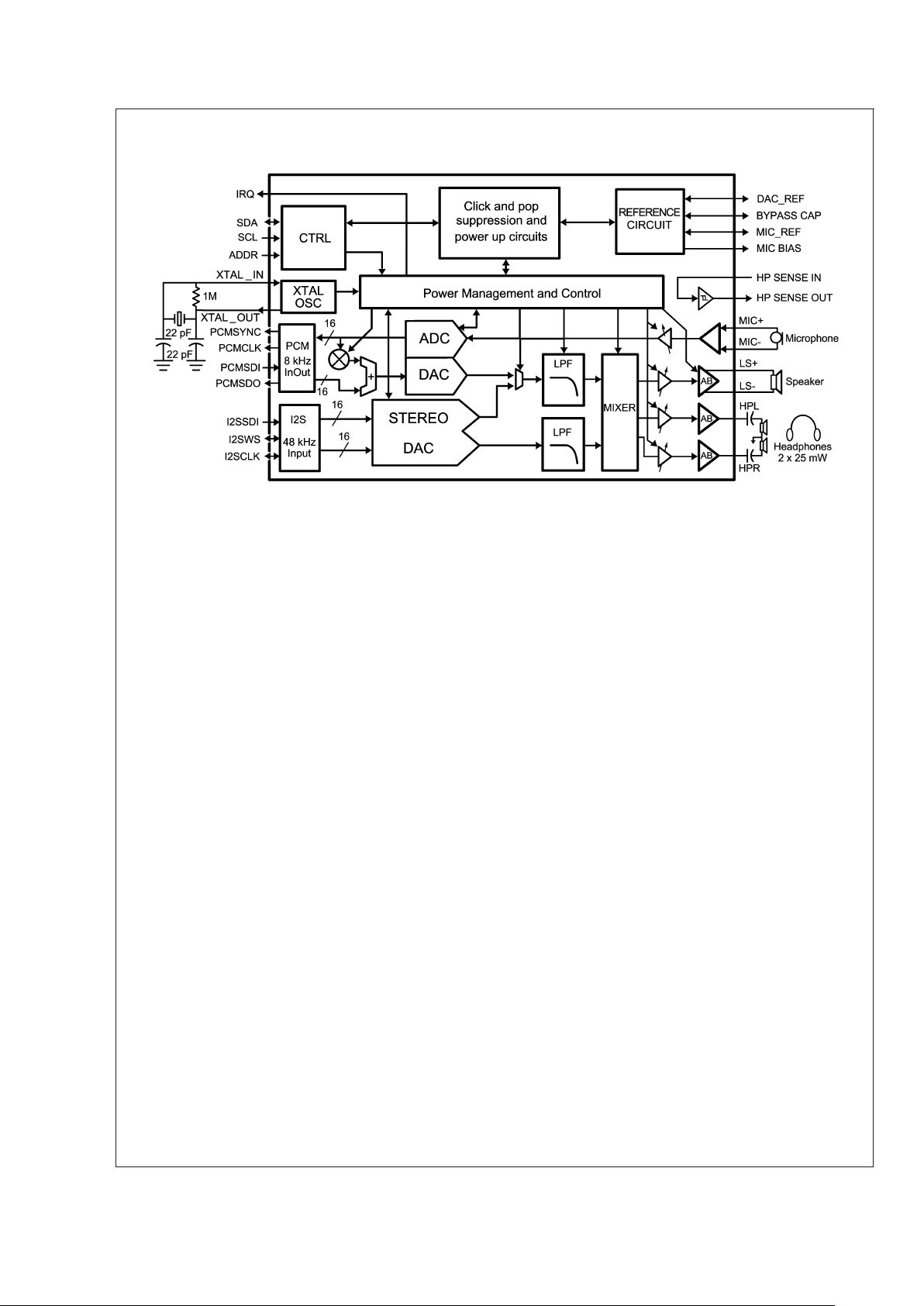
Typical Application
20072003
FIGURE 1. Typical I2S + Voice codec application circuit for mobile phones
LM4930
www.national.com 2
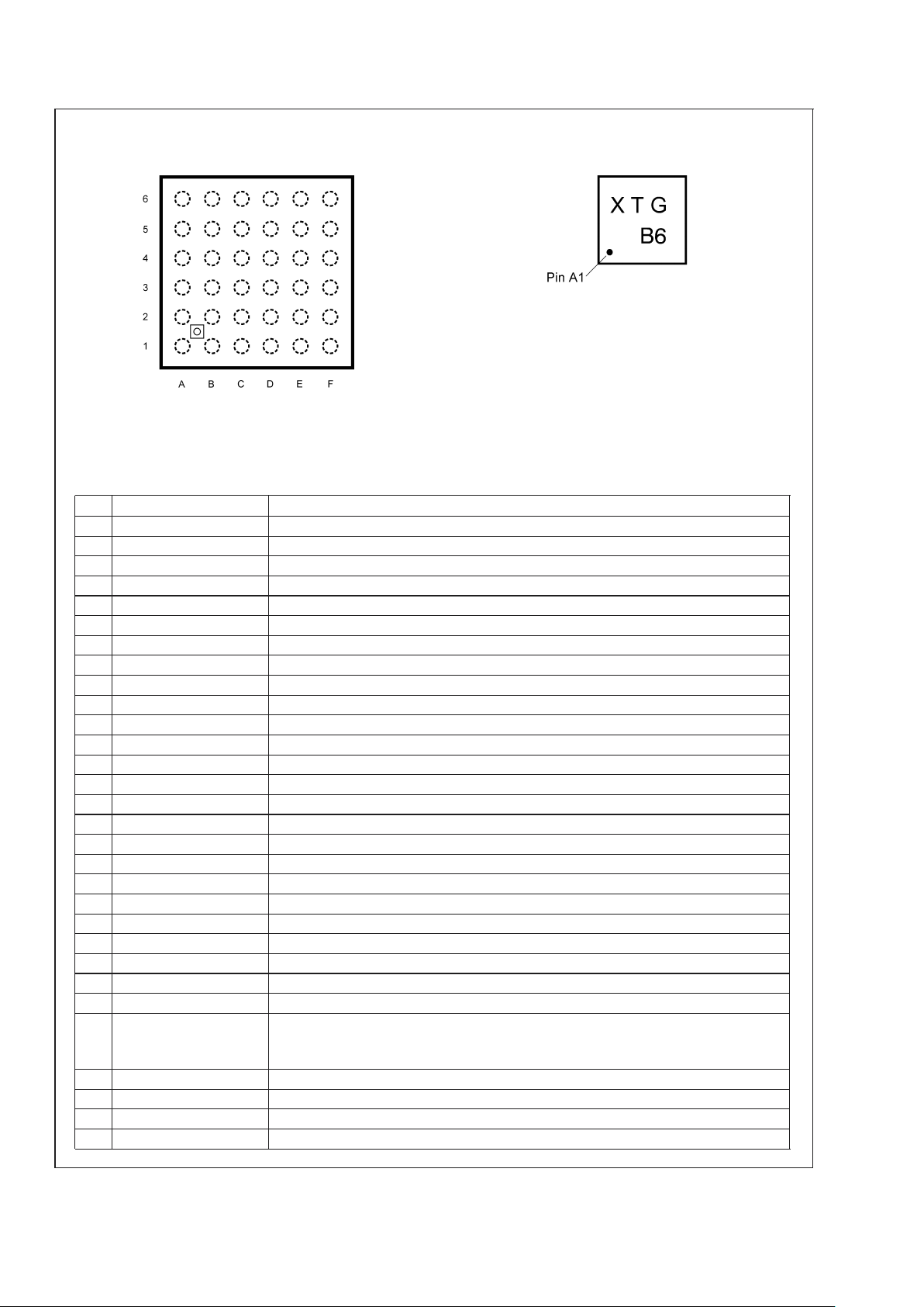
Connection Diagrams
36-Bump micro SMD micro SMD Marking
20072002
Top View
Order Number LM4930ITL
See NS Package Number MKT-TLA36KRA
20072056
Top View
X - Date Code
T - Die Traceability
G - Boomer Family
B6 - LM4930ITL
Pin Descriptions
A1 MIC_P Microphone positive differential input
A2 MIC_N Microphone negative differential input
A3 AVDD_MIC Analog V
dd
for microphone preamp
A4 DAC_REF D/A converter reference voltage
A5 SDA Two-wire control interface serial data pin
A6 SCL Two-wire control interface serial clock pin
B1 AGND_MIC Analog ground for microphone preamp
B2 MIC_BIAS Microphone bias supply output (2V)
B3 MIC_REF Internal fixed-reference bypass capacitor decoupling pin
B4 ADDR Control bus address select pin
B5 PCM_SDI PCM serial data in
B6 PCM_CLK PCM Serial clock pin
C1 AVDD_HP Analog V
dd
for headphone amplifier
C2 NC No Connect
C3 BYPASS Half-supply bypass capacitor decoupling pin
C4 PCM_SYNC PCM Frame sync pin
C5 I2S_DATA I
2
S serial data input
C6 DGND_D Digital ground
D1 HP_L Headphone amplifier connection (Left)
D2 HP_R Headphone amplifier connection (Right)
D3 HPSENSE_IN Connection for sense pin of headphone jack
D4 PCM_SDO PCM serial data out
D5 I2S_CLK I
2
S serial bit clock
D6 DVDD_D Digital V
dd
E1 AGND_HP Analog ground for headphone amplifier
E2 LS- Loudspeaker amplifier BTL negative out (-)
E3 HPSENSE_OUT Logic output pin to indicate headphone connection status. Outputs logic high when
HPSENSE_IN is high and outputs logic low when HPSENSE_IN is low. See Figure 5
for suggested application circuit
E4 IRQ LM4930 mode status indicator pin
E5 I2S_WS I
2
S word select
E6 XTAL_OUT Negative feedback source for external crystal MCLK
F1 AGND_LS Analog ground for loudspeaker amplifier
LM4930
www.national.com3
Pin Descriptions (Continued)
F2 LS+ Loudspeaker amplifier BTL positive out (+)
F3 AVDD_LS Analog V
DD
for loudspeaker amplifier
F4 DGND_X Digital ground
F5 DVDD_X Digital V
DD
F6 MCLK/XTAL_IN 12.288MHz or 24.576MHz Master Clock from crystal (via XTAL OUT) or external source
SYSTEM CONTROL REGISTERS
The LM4930 is controlled with a two-wire serial interface. This interface is used to configure the operating mode, digital interfaces,
and delta-sigma modulators. The LM4930 is controlled by writing information into a series of write-only registers, each with its own
unique 7 bit address. The following registers are programmable:
Basic Config Register
This register is used to configure the I2S and PCM interfaces as well as the 48kHz DAC module. The 7 bit address for the
BASICCONFIG register is XX10000. (X=0ifADDR is set to logic 0) (X=1ifADDR is set to logic 1)
BASIC CONFIGURATION (XX1000). (Set = logic 1, Clear = logic 0)
BIT 15 14 131211109876543210
RESET 0 0 00000000000000
Address Register Description
3:0 MODE The LM4930 can be placed in one of several modes that dictate the basic operation. When a
new mode is selected the LM4930 will change operation silently and will reconfigure the
power management profile automatically. The modes are described as follows: (Note 14)
Mode Mono Speaker
Amplifier Source
Headphone Left
Source
Headphone Right
Source
Comment
0000 None None None Powerdown mode
0001 None None None Standby Mode
0010 Voice None None Mono speaker
mode
0011 None Voice Voice Headphone call
mode
0100 Voice Voice Voice Conference call
mode
0101 Audio (L+R) None None L+R mixed to
mono speaker
0110 None Audio (Left) Audio (Right) Headphone
stereo audio
0111 Audio (L+R) Audio (Left) Audio (Right) L+R mixed to
mono speaker +
stereo headphone
audio
1000 Audio (Left) Voice Voice Mixed Mode
1001 Voice + Audio
(Left)
Voice Voice Mixed mode
1010 Voice Audio (Left) Audio (Left) Mixed Mode
4 SOFT_RESET Resets the LM4930, excluding the control registers
5 PCM_LONG If set the PCM interface uses a long frame sync. (Note 12)
6 PCM_COMPANDED If set the 8 MSBs are presumed to be companded data and the 8 LSBs are ignored. (Note
12)
7 PCM_LAW If set, the companded G711 data is set to be A-law, else m-law is assumed (Note 12)
8:9 PCM_SYNC_MODE Sets 1 (00h), 2 (01h) or 4(10h) 16 bit frames per sync. The PCM_SDO pin is tri-stated during
the latter frames. (Note 12)
LM4930
www.national.com 4
SYSTEM CONTROL REGISTERS (Continued)
Basic Config Register (Continued)
10 PCM_ALWAYS_ON This bit should be set if another codec is using the PCM bus. When set, the LM4930 will
drive the clock and sync signals in all modes except Powerdown (Note 12)
11 I2S_M/S I2S master or slave select. If set then I2S = master. Cleared = slave
12 I2S_RES I2S resolution select. If set then 32 bits per frame. If cleared then 16 bits per frame
13 RSVD RESERVED (Note 13)
14 RSVD RESERVED (Note 13)
15 RSVD RESERVED (Note 13)
Voice/Test Config Registers
This register configures the voiceband codec, sidetone attenuation, and selected control functions. The 7 bit address for the
VOICE TESTCONFIG register is XX10001. (X=0ifADDR is set to logic 0) (X=1ifADDR is set to logic 1)
VOICETESTCONFIG (XX10001). (Set = logic 1, Clear = logic 0)
BIT 15 14 131211109876543210
RESET 0 0 00000000000000
Address Register Description
0 CLASS If set, configures the chip for use with an external class D or linear amplifier and turns the
BTL speaker output into a buffer. (Note 12)
4:1 SIDESTONE_ATTEN Programs the attenuation of the digital sidetone. Attenuation is set as follows:
4:1 Sidetone
Attenuation
4:1 Sidetone Attenuation
0000 Mute 1000 -9dB
0001 -30dB 1001 -6dB
0010 -27dB 1010 -3dB
0011 -24dB 1011 0dB
0100 -21dB 1100 Mute
0101 -18dB 1101 Mute
0110 -15dB 1110 Mute
0111 -12dB 1111 Mute
5 AUTOSIDE This feature is included for use with the mono speaker in hands-free applications where
sidetones may not be desirable. If set, the sidetone is always muted in voice over mono
speaker modes (0010, 0100, 1001, and 1010), otherwise the sidetone is present at whatever
level is set in the gain control register
6 CLOCK_DIV If set, allows for the use of a 24.576MHz crystal. Default setting is for 12.288MHz crystal.
(Note 12)
7 ZXD_DISABLE Disables the zero crossing detect in the stereo DAC to guarantee immediate mode changes
rather than waiting for a zero cross. (Note 11)
8:9 RSVD RESERVED (Note 13)
10:11 CAP_SIZE Set to accomodate different bypass capacitor values to give correct turn-off delay and
click/pop performance. Value is set as follows: (Note 12)
10:11 Delay Bypass Capacitor Size
00 25ms 0.1µF
01 50ms 0.39µF
10 85ms 1µF
11 RESERVED RESERVED
12 ZXDS_SLOW If set, this forces the stereo DAC outputs to wait for a zero crossing before powering down
13 MUTE_LS If set, mutes the loudspeaker amplifier in any mode where it is not already muted
14 MUTE_HP If set, mutes the headphone amplifier in any mode where it is not already muted
15 MUTE_MIC If set, mutes the microphone preamp
LM4930
www.national.com5
SYSTEM CONTROL REGISTERS (Continued)
Gain Config Registers
This register is used to control the gain of the headphone amplifier, the loudspeaker amplifier, and the microphone preamplifier. The 7 bit address for the GAINCONFIG register is XX10010. (X=0ifADDR is set to logic 0) (X=1ifADDR is set
to logic 1)
GAINCONFIG (XX10010). (Set = logic 1, Clear = logic 0)
BIT 15 14 131211109876543210
RESET 0 0 00000000000000
Address Register Description
4:0 LOUDSPKR_GAIN Programs the gain of the loudspeaker amplifier. Gain is set as follows:
4:0 Loudspeaker
Gain
4:0 Loudspeaker Gain
00000 -34.5dB 10000 -10.5dB
00001 -33dB 10001 -9dB
00010 -31.5dB 10010 -7.5dB
00011 -30dB 10011 -6dB
00100 -28.5dB 10100 -4.5dB
00101 -27dB 10101 -3dB
00110 -25.5dB 10110 -1.5dB
00111 -24dB 10111 0dB
01000 -22.5dB 11000 1.5dB
01001 -21dB 11001 3dB
01010 -19.5dB 11010 4.5dB
01011 -18dB 11011 6dB
01100 -16.5dB 11100 7.5dB
01101 -15dB 11101 9dB
01110 -13.5dB 11110 10.5dB
01111 -12dB 11111 12dB
9:5 HP_GAIN Programs the gain of the headphone amplifier. Gain is set as follows:
9:5 Headphone Gain 9:5 Headphone Gain
00000 -46dB 10000 -22.5dB
00001 -45dB 10001 -21dB
00010 -43.5dB 10010 -19.5dB
00011 -42db 10011 -18dB
00100 -40.5dB 10100 -16.5dB
00101 -39dB 10101 -15dB
00110 -37.5dB 10110 -13.5dB
00111 -36dB 10111 -12dB
01000 -34.5dB 11000 -10.5dB
01001 -33dB 11001 -9dB
01010 -31.5dB 11010 -7.5dB
01011 -30dB 11011 -6dB
01100 -28.5dB 11100 -4.5dB
01101 -27dB 11101 -3dB
01110 -25.5dB 11110 -1.5dB
01111 -24dB 11111 0dB
13:10 MIC_GAIN Programs the gain of the microphone amplifier. Gain is set as follows:
LM4930
www.national.com 6
SYSTEM CONTROL REGISTERS (Continued)
Gain Config Registers (Continued)
13:10 Mic Preamp Gain
0000 17dB
0001 19dB
0010 21dB
0011 23dB
0100 25dB
0101 27dB
0110 29dB
0111 31dB
1000 33dB
1001 35dB
1010 37dB
1011 39dB
1100 41dB
1101 43dB
1110 45dB
1111 47dB
15:14 RSVD RESERVED (Note 13)
20072009
Two-wire control Interface Timing Diagram
FIGURE 2.
20072008
PCM Receive Timing Diagram
FIGURE 3.
LM4930
www.national.com7
20072007
I2S Transmit Timing Diagram
FIGURE 4.
LM4930
www.national.com 8
Absolute Maximum Ratings (Notes 1,
2)
If Military/Aerospace specified devices are required,
please contact the National Semiconductor Sales Office/
Distributors for availability and specifications.
Analog Supply Voltage 6.0V
Digital Storage Supply Voltage 6.0V
Storage temperature -65˚C to +150˚C
Power Dissipation (Note 3) Internally Limited
ESD Susceptibility
Human Body Model (Note 4) 2000V
Machine Model (Note 5) 200V
Junction temperature 150˚C
Thermal Resistance
θ
JA
- TLA36KRA 105˚C/W
Operating Ratings (Note 3)
Temperature Range
T
MIN
≤ TA≤ T
MAX
−30˚C ≤ TA≤ +85˚C
Supply Voltage
DV
DD
(Note 8) 2.6V - 4.5V
AV
DD
(Note 8) 2.6V - 5.5V
Electrical Characteristics DVDD= 3.3V, AVDD= 5V, R
LHP
=32Ω,R
LHF
=8Ω
(Notes 1, 2, 8)
The following specifications apply for the circuit shown in Figure 1, unless otherwise specified. Limits apply for TA= 25˚C.
Symbol Parameter Conditions LM4930 Units
(Limits)
Typical
(Note 6)
Limits
(Notes 7,
15)
DI
DD
Digital Power Supply Current
f
MCLK
= 12.288MHz
Output Mode = "0010"
Output Mode = "0011"
Output Mode = "0100"
2
Output Mode = "0101"
Output Mode = "0110"
Output Mode = "0111"
4.4
Output Mode = "1000"
Output Mode = "1001"
Output Mode = "1010"
4.9 8 mA (max)
AI
DD
Analog Power Supply Quiescent
Current
f
MCLK
= 12.288MHz; No Load
Output Mode = "0010" 7.0
Output Mode = "0011" 6.3
Output Mode = "0100" 8.0
Output Mode = "0101" 8.2
Output Mode = "0110" 7.4
Output Mode = "0111" 8.7
Output Mode = "1000"
Output Mode = "1001"
Output Mode = "1010"
9.5 14 mA (max)
DI
SD
Digital Powerdown Current f
MCLK
= 12.288MHz
Output Mode = "0000" Powerdown Mode
1 7 µA (max)
AI
SD
Analog Powerdown Current f
MCLK
= 12.288MHz
Output Mode = "0000" Powerdown Mode
1 2 µA (max)
DI
ST
Digital Standby Current f
MCLK
= 12.288MHz
Output Mode = "0001"Standby Mode
1.4 2 mA (max)
AI
ST
Analog Standby Current f
MCLK
= 12.288MHz
Output Mode = "0001"Standby Mode
230 1000 µA (max)
V
FS_LS
Full-Scale Output Voltage
(Mono speaker amplifier)
CLASS = 0; 0dB gain setting; 8Ω BTL
load (Note 10)
2.5 V
P-P
V
FS_HP
Full-Scale Output Voltage
(Headphone amplifier)
0dB gain setting; 32Ω Stereo Load (Note
10)
2.5 V
P-P
LM4930
www.national.com9
Electrical Characteristics DVDD= 3.3V, AVDD= 5V, R
LHP
=32Ω,R
LHF
=8Ω
(Notes 1, 2, 8) (Continued)
The following specifications apply for the circuit shown in Figure 1, unless otherwise specified. Limits apply for TA= 25˚C.
Symbol Parameter Conditions LM4930 Units
(Limits)
Typical
(Note 6)
Limits
(Notes 7,
15)
V
MIC_BIAS
Mic Bias Voltage 2.0 V
THD+N Headphone Amplifier Total
Harmonic Motion Distortion +
Noise
f
IN
= 1 kHz, P
OUT
= 7.5mW; 32Ω Stereo
Load
0.07 %
P
OHP
Headphone Amplifier Output
Power
THD+N = 0.5%, f
OUT
= 1kHz 27 20 mW (min)
P
OLS
Mono Speaker Amplifier Output
Power
THD+N = 3%, f
OUT
= 1kHz 1 W
PSRR Power Supply Rejection Ratio C
BYPASS
= 1.0µF
C
DAC_REF
= 1.0µF
V
RIPPLE
= 200mV
P-P
@
217Hz, MIC_P,
MIC_N terminated with 10Ω to ground
55 45 dB (min)
SNR
(Voice)
Signal-to-Noise Ratio
(Voice Audio Path)
Signal = Vo at f = 1kHz
@
1% THD+N,
32Ω Stereo Load; Noise = digital zero,
A-weighted, 0dB gain setting
72 dB
SNR
(Music)
Signal-to-Noise Ratio (Music
Audio Path)
Signal = Vo at f = 1kHz
@
1% THD+N,
32Ω Stereo Load; Noise = digital zero,
A-weighted; 0dB gain setting
86 dB
DR
(Voice)
Dynamic Range (Voice Audio
Path)
Signal = Vo at f = 1kHz
@
1% THD+N,
32Ω Stereo Load; Noise for -60dBFS
digital input; A-weighted; 0dB gain setting
72 dB
DR
(Music)
Dynamic Range (Music Audio
Path)
Signal = Vo at f=1kHz
@
1% THD+N, 32Ω
Stereo Load; Noise for -60dBFS digital
input; A-weighted, 0dB gain setting
86 dB
SNR
ADC
Signal-to-Noise Ratio
(Voice ADC Path)
Reference signal = 0dBFS
MIC_P, MIC_N terminated with 10Ω to
ground;
A-weighted; 47dB MIC preamp gain
setting
75 dB
DR
ADC
Dynamic Range
(Voice ADC Path)
Reference signal = 0dBFS
Noise for -60dBFS digital input;
A-weighted; 47dB MIC preamp gain
setting
75 dB
X
TALK
Stereo Channel-to-Channel
Crosstalk
fS= 48kHz, fIN= 1kHz sinewave at
-3dB
FS
75 dB
V
MIC-IN
Maximum Differential MIC Input
Voltage
17dB MIC Preamp gain setting 570 mV
P-P
R
VDAC
Voice DAC Ripple 300Hz - 3.3kHz through head-phone
output.
+/-0.15 +/-0.2 dB (max)
R
VADC
Voice ADC Ripple 300Hz - 3.3kHz through head-phone
output.
+/-0.25 +/-0.3 dB (max)
PB
VDAC
Voice DAC Passband -3dB Point 3.46 kHz
SBA
VDAC
Voice DAC Stopband Attenuation Above 4kHz 72 dB
UPB
VADC
Voice ADC Upper Passband
Cutoff Frequency.
Upper -3dB Point 3.47 kHz
LM4930
www.national.com 10
 Loading...