

NSC LM4890MX, LM4890MWC, LM4890MMX, LM4890MM, LM4890LDX Datasheet
...
LM4890
1 Watt Audio Power Amplifier
General Description
The LM4890 is an audio power amplifier primarily designed
for demanding applications in mobile phones and other portable communication device applications. It is capable of
delivering 1 watt of continuous average power to an 8Ω BTL
load with less than 1% distortion (THD+N) from a 5V
DC
power supply.
Boomer audio power amplifiers were designed specifically to
provide high quality output power with a minimal amount of
external components. The LM4890 does not require output
coupling capacitors or bootstrap capacitors, and therefore is
ideally suited for mobile phone and other low voltage applications where minimal power consumption is a primary requirement.
The LM4890 features a low-power consumption shutdown
mode, which is achieved by driving the shutdown pin with
logic low. Additionally, the LM4890 features an internal thermal shutdown protection mechanism.
The LM4890 contains advanced pop & click circuitry which
eliminates noises which would otherwise occur during
turn-on and turn-off transitions.
The LM4890 is unity-gain stable and can be configured by
external gain-setting resistors.
Key Specifications
j
PSRR at 217Hz, VDD= 5V (Fig. 1) 62dB(typ.)
j
Power Output at 5.0V & 1% THD 1W(typ.)
j
Power Output at 3.3V & 1% THD 400mW(typ.)
j
Shutdown Current 0.1µA(typ.)
Features
n Available in space-saving packages: micro SMD, MSOP,
SOIC, and LLP
n Ultra low current shutdown mode
n BTL output can drive capacitive loads
n Improved pop & click circuitry eliminates noises during
turn-on and turn-off transitions
n 2.2 - 5.5V operation
n No output coupling capacitors, snubber networks or
bootstrap capacitors required
n Thermal shutdown protection
n Unity-gain stable
n External gain configuration capability
Applications
n Mobile Phones
n PDAs
n Portable electronic devices
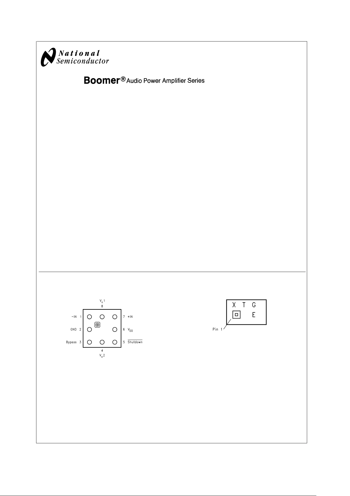
Connection Diagrams
8 Bump micro SMD 8 bump micro SMD Marking
20019223
Top View
Order Number LM4890IBP, LM4890IBPX
See NS Package Number BPA08DDB
20019270
Top View
X - Date Code
T - Die Traceability
G - Boomer Family
E - LM4890IBP
Boomer®is a registered trademark of National Semiconductor Corporation.
May 2003
LM4890 1 Watt Audio Power Amplifier
© 2003 National Semiconductor Corporation DS200192 www.national.com
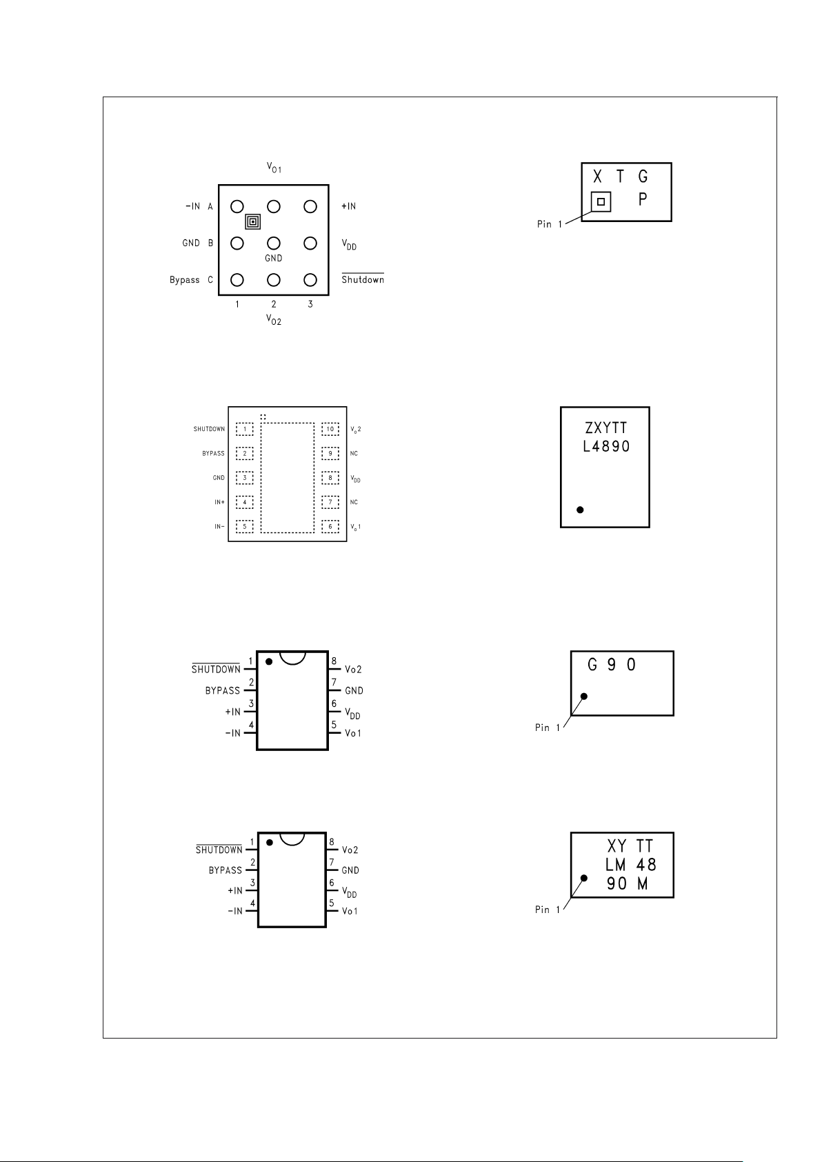
Connection Diagrams (Continued)
9 Bump micro SMD 9 Bump micro SMD Marking
200192C1
Top View
Order Number LM4890IBL, LM4890IBLX
See NS Package Number BLA09AAB
200192C2
Top View
X - Date Code
T - Die Traceability
G - Boomer Family
P - LM4890IBL
LLP Package 10 Pin LLP Marking
200192C7
Top View
Order Number LM4890LD
See NS Package Number LDA10B
200192C6
Top View
Z - Assembly Plant Date Code (M for Malacca)
XY - Digit Date Code
TT - Die Traceability
L4890 - LM4890LD
Mini Small Outline (MSOP) Package MSOP Marking
20019236
Top View
Order Number LM4890MM
See NS Package Number MUA08A
20019271
Top View
G - Boomer Family
90 - LM4890MM
Small Outline (SO) Package SO Marking
20019235
Top View
Order Number LM4890M
See NS Package Number M08A
20019272
Top View
XY - Date Code
TT - Die Traceability
Bottom 2 lines - Part Number
LM4890
www.national.com 2
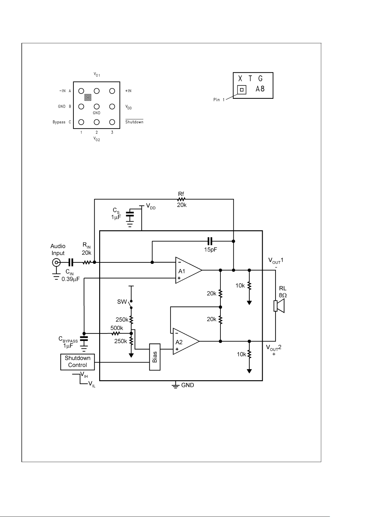
Connection Diagrams (Continued)
9 Bump micro SMD 9 Bump micro SMD Marking
200192C1
Top View
Order Number LM4890ITL, LM4890ITLX
See NS Package Number TLA09AAA
200192D0
Top View
X - Date Code
T - Die Traceability
G - Boomer Family
A8 - LM4890ITL
Typical Application
20019201
FIGURE 1. Typical Audio Amplifier Application Circuit
LM4890
www.national.com3
Absolute Maximum Ratings (Note 2)
If Military/Aerospace specified devices are required,
please contact the National Semiconductor Sales Office/
Distributors for availability and specifications.
Supply Voltage (Note 11) 6.0V
Storage Temperature −65˚C to +150˚C
Input Voltage −0.3V to V
DD
+0.3V
Power Dissipation (Note 3) Internally Limited
ESD Susceptibility (Note 4) 2000V
Junction Temperature 150˚C
Thermal Resistance
θ
JC
(SOP) 35˚C/W
θ
JA
(SOP) 150˚C/W
θ
JA
(8 Bump micro SMD, Note 12) 220˚C/W
θ
JA
(9 Bump micro SMD, Note 12) 180˚C/W
θ
JC
(MSOP) 56˚C/W
θ
JA
(MSOP) 190˚C/W
θ
JA
(LLP) 220˚C/W
Soldering Information
See AN-1112 "microSMD Wafers Level Chip Scale
Package."
See AN-1187 "Leadless Leadframe Package (LLP)."
Operating Ratings
Temperature Range
T
MIN
≤ TA≤ T
MAX
−40˚C ≤ TA≤ 85˚C
Supply Voltage 2.2V ≤ V
DD
≤ 5.5V
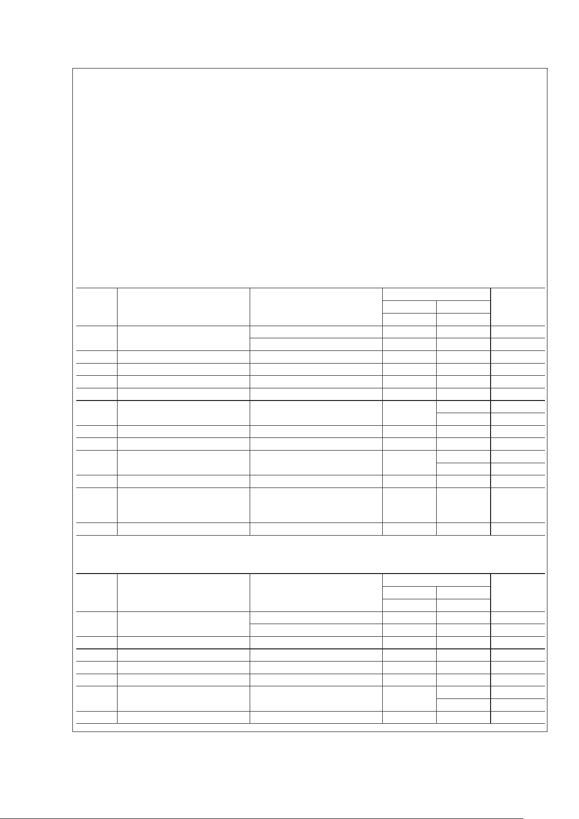
Electrical Characteristics VDD=5V (Notes 1, 2, 8)
The following specifications apply for the circuit shown in Figure 1 unless otherwise specified. Limits apply for T
A
= 25˚C.
Symbol Parameter Conditions
LM4890
Units
(Limits)
Typical Limit
(Note 6) (Notes 7, 9)
I
DD
Quiescent Power Supply Current VIN= 0V, Io= 0A, No Load 4 8 mA (max)
V
IN
= 0V, Io= 0A, 8Ω Load 5 10 mA (max)
I
SD
Shutdown Current V
SHUTDOWN
= 0V 0.1 2.0 µA (max)
V
SDIH
Shutdown Voltage Input High 1.2 V (min)
V
SDIL
Shutdown Voltage Input Low 0.4 V (max)
V
OS
Output Ofsett Voltage 7 50 mV (max)
R
OUT-GND
Resistor Output to GND (Note 10)
8.5
9.7 kΩ (max)
7.0 kΩ (min)
P
o
Output Power ( 8Ω ) THD = 2% (max);f=1kHz 1.0 0.8 W
T
WU
Wake-up time 170 220 ms (max)
T
SD
Thermal Shutdown Temperature
170
150 ˚C (min)
190 ˚C (max)
THD+N Total Harmonic Distortion+Noise P
o
= 0.4 Wrms; f = 1kHz 0.1 %
PSRR Power Supply Rejection Ratio
(Note 14)
V
ripple
= 200mV sine p-p
Input Terminated with 10 ohms to
ground
62 (f =
217Hz)
66 (f = 1kHz)
55 dB (min)
T
SDT
Shut Down Time 8 Ω load 1.0 ms (max)
Electrical Characteristics VDD=3V (Notes 1, 2, 8)
The following specifications apply for the circuit shown in Figure 1 unless otherwise specified. Limits apply for T
A
= 25˚C.
Symbol Parameter Conditions
LM4890
Units
(Limits)
Typical Limit
(Note 6) (Notes 7, 9)
I
DD
Quiescent Power Supply Current VIN= 0V, Io= 0A, No Load 3.5 7 mA (max)
V
IN
= 0V, Io= 0A, 8Ω Load 4.5 9 mA (max)
I
SD
Shutdown Current V
SHUTDOWN
= 0V 0.1 2.0 µA (max)
V
SDIH
Shutdown Voltage Input High 1.2 V(min)
V
SDIL
Shutdown Voltage Input Low 0.4 V(max)
V
OS
Output Offset Voltage 7 50 mV (max)
R
OUT-GND
Resistor Output to Gnd (Note 10)
8.5
9.7 kΩ (max)
7.0 kΩ (min)
T
WU
Wake-up time 120 180 ms (max)
LM4890
www.national.com 4
Electrical Characteristics VDD=3V(Notes 1, 2, 8)
The following specifications apply for the circuit shown in Figure 1 unless otherwise specified. Limits apply for T
A
=
25˚C. (Continued)
Symbol Parameter Conditions
LM4890
Units
(Limits)
Typical Limit
(Note 6) (Notes 7, 9)
P
o
Output Power ( 8Ω ) THD = 1% (max); f = 1kHz 0.31 0.28 W
T
SD
Thermal Shutdown Temperature
170
150 ˚C(min)
190 ˚C(max)
THD+N Total Harmonic Distortion+Noise P
o
= 0.15Wrms; f = 1kHz 0.1 %
PSRR Power Supply Rejection Ratio
(Note 14)
V
ripple
= 200mV sine p-p
Input terminated with 10 ohms to
ground
56 (f =
217Hz)
62 (f = 1kHz)
45 dB(min)
Electrical Characteristics VDD= 2.6V (Notes 1, 2, 8)
The following specifications apply for for the circuit shown in Figure 1 unless otherwise specified. Limits apply for T
A
= 25˚C.
Symbol Parameter Conditions
LM4890
Units
(Limits)
Typical Limit
(Note 6) (Notes 7, 9)
I
DD
Quiescent Power Supply Current VIN= 0V, Io= 0A, No Load 2.6 mA (max)
I
SD
Shutdown Current V
SHUTDOWN
= 0V 0.1 µA (max)
P
0
Output Power ( 8Ω )
Output Power ( 4Ω )
THD = 1% (max);f=1kHz
THD = 1% (max);f=1kHz
0.2
0.22
W
W
THD+N Total Harmonic Distortion+Noise P
o
= 0.1Wrms; f = 1kHz 0.08 %
PSRR Power Supply Rejection Ratio
(Note 14)
V
ripple
= 200mV sine p-p
Input Terminated with 10 ohms to
ground
44 (f =
217Hz)
44 (f = 1kHz)
dB
Note 1: All voltages are measured with respect to the ground pin, unless otherwise specified.
Note 2: Absolute Maximum Ratings indicate limits beyond which damage to the device may occur. Operating Ratings indicate conditions for which the device is
functional, but do not guarantee specific performance limits. Electrical Characteristics state DC andAC electrical specifications under particular test conditions which
guarantee specific performance limits. This assumes that the device is within the Operating Ratings. Specifications are not guaranteed for parameters where no limit
is given, however, the typical value is a good indication of device performance.
Note 3: The maximum power dissipation must be derated at elevated temperatures and is dictated by T
JMAX
, θJA, and the ambient temperature TA. The maximum
allowable power dissipation is P
DMAX
=(T
JMAX–TA
)/θJAor the number given inAbsolute Maximum Ratings, whichever is lower. For the LM4890, see power derating
curves for additional information.
Note 4: Human body model, 100 pF discharged through a 1.5 kΩ resistor.
Note 5: Machine Model, 220 pF–240 pF discharged through all pins.
Note 6: Typicals are measured at 25˚C and represent the parametric norm.
Note 7: Limits are guaranteed to National’s AOQL (Average Outgoing Quality Level).
Note 8: For micro SMD only, shutdown current is measured in a Normal Room Environment. Exposure to direct sunlight will increase I
SD
by a maximum of 2µA.
Note 9: Datasheet min/max specification limits are guaranteed by design, test, or statistical analysis.
Note 10: ROUT is measured from each of the output pins to ground. This value represents the parallel combination of the 10k ohm output resistors and the two 20k
ohm resistors.
Note 11: If the product is in shutdown mode and V
DD
exceeds 6V (to a max of 8V VDD), then most of the excess current will flow through the ESD protection circuits.
If the source impedance limits the current to a max of 10 ma, then the part will be protected. If the part is enabled when V
DD
is greater than 5.5V and less than 6.5V,
no damage will occur, although operational life will be reduced. Operation above 6.5V with no current limit will result in permanent damage.
Note 12: All bumps have the same thermal resistance and contribute equally when used to lower thermal resistance. All bumps must be connected to achieve
specified thermal resistance.
Note 13: Maximum power dissipation (P
DMAX
) in the device occurs at an output power level significantly below full output power. P
DMAX
can be calculated using
Equation 1 shown in the Application section. It may also be obtained from the power dissipation graphs.
Note 14: PSRR is a function of system gain. Specifications apply to the circuit in Figure 1 where A
V
= 2. Higher system gains will reduce PSRR value by the amount
of gain increase. A system gain of 10 represents a gain increase of 14dB. PSRR will be reduced by 14dB and applies to all operating voltages.
LM4890
www.national.com5

External Components Description (Figure 1)
Components Functional Description
1. R
IN
Inverting input resistance which sets the closed-loop gain in conjunction with Rf. This resistor also forms a
high pass filter with C
IN
at fC= 1/(2π RINCIN).
2. C
IN
Input coupling capacitor which blocks the DC voltage at the amplifier’s input terminals. Also creates a
highpass filter with R
IN
at fc= 1/(2π RINCIN). Refer to the section, Proper Selection of External
Components, for an explanation of how to determine the value of C
IN
.
3. R
f
Feedback resistance which sets the closed-loop gain in conjunction with RIN.
4. C
S
Supply bypass capacitor which provides power supply filtering. Refer to the section, Power Supply
Bypassing, for information concerning proper placement and selection of the supply bypass capacitor,
C
BYPASS
.
5. C
BYPASS
Bypass pin capacitor which provides half-supply filtering. Refer to the section, Proper Selection of External
Components, for information concerning proper placement and selection of C
BYPASS
.
LM4890
www.national.com 6
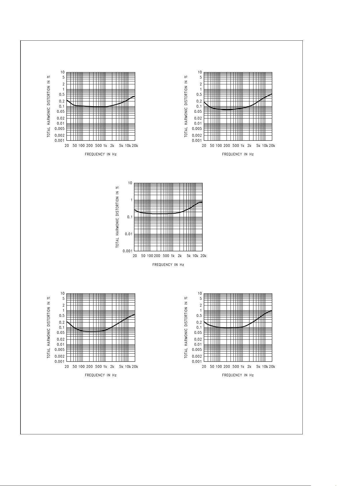
Typical Performance Characteristics
THD+N vs Frequency
at V
DD
= 5V, 8Ω RL, and PWR = 250mW, AV=2
THD+N vs Frequency
at VDD= 3.3V, 8Ω RL, and PWR = 150mW, AV=2
20019237 20019238
THD+N vs Frequency
at V
DD
= 3V, RL=8Ω, PWR = 250mW, AV=2
20019290
THD+N vs Frequency
@
VDD= 2.6V, RL=8Ω, PWR = 100mW, AV=2
THD+N vs Frequency
@
VDD= 2.6V, RL=4Ω, PWR = 100mW, AV=2
20019239 20019240
LM4890
www.national.com7
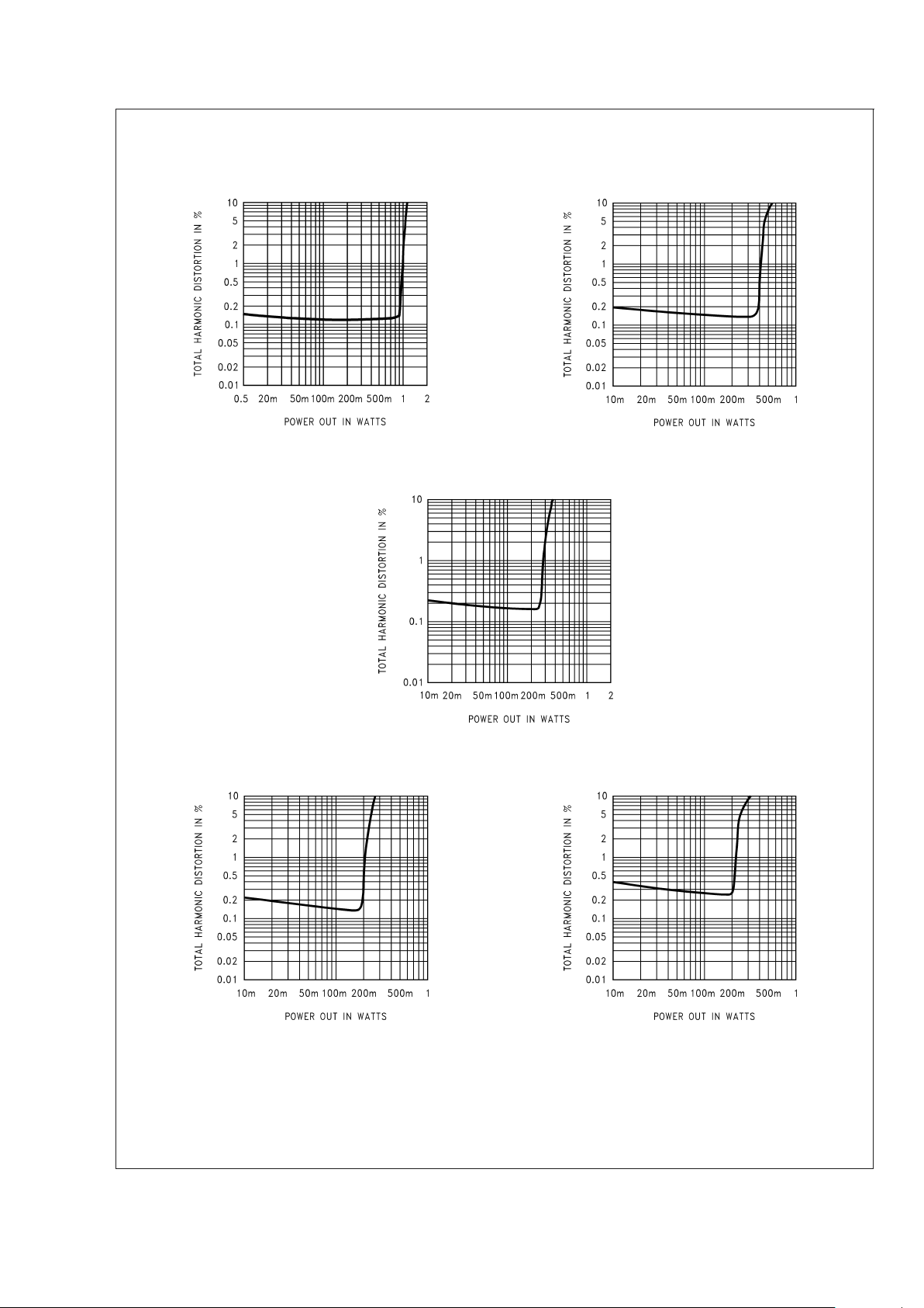
Typical Performance Characteristics (Continued)
THD+N vs Power Out
@
VDD= 5V, RL=8Ω, 1kHz, AV=2
THD+N vs Power Out
@
VDD= 3.3V, RL=8Ω, 1kHz, AV=2
200192C9
20019242
THD+N vs Power Out
@
VDD= 3V, RL=8Ω, 1kHz, AV=2
20019291
THD+N vs Power Out
@
VDD= 2.6V, RL=8Ω, 1kHz, AV=2
THD+N vs Power Out
@
VDD= 2.6V, RL=4Ω, 1kHz, AV=2
20019243 20019244
LM4890
www.national.com 8
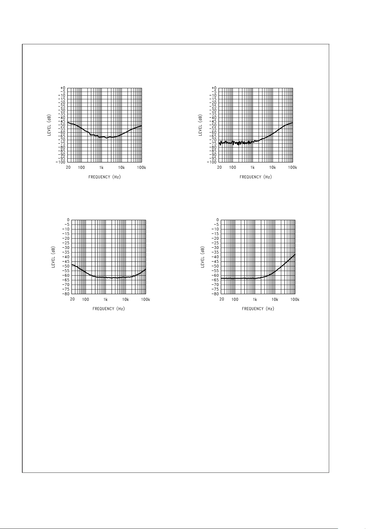
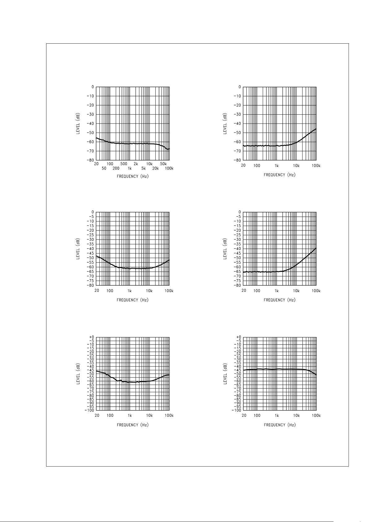
Typical Performance Characteristics (Continued)
Power Supply Rejection Ratio (PSRR)
@
AV=2
V
DD
= 5V, V
ripple
= 200mvp-p
R
L
=8Ω,RIN=10Ω
Power Supply Rejection Ratio (PSRR)
@
AV=2
V
DD
= 5V, V
ripple
= 200mvp-p
R
L
=8Ω,RIN= Float
20019245 20019273
Power Supply Rejection Ratio (PSRR)@AV=4
V
DD
= 5V, V
ripple
= 200mvp-p
R
L
=8Ω,RIN=10Ω
Power Supply Rejection Ratio (PSRR)
@
AV=4
V
DD
= 5V, V
ripple
= 200mvp-p
R
L
=8Ω,RIN= Float
200192A9 200192B8
LM4890
www.national.com9
Typical Performance Characteristics (Continued)
Power Supply Rejection Ratio (PSRR)
@
AV=2
V
DD
= 3V, V
ripple
= 200mvp-p,
R
L
=8Ω,RIN=10Ω
Power Supply Rejection Ratio (PSRR)
@
AV=2
V
DD
= 3V, V
ripple
= 200mvp-p,
R
L
=8Ω,RIN= Float
200192C5
20019293
Power Supply Rejection Ratio (PSRR)@AV=4
V
DD
= 3V, V
ripple
= 200mvp-p,
R
L
=8Ω,RIN=10Ω
Power Supply Rejection Ratio (PSRR)
@
AV=4
V
DD
= 3V, V
ripple
= 200mvp-p,
R
L
=8Ω,RIN= Float
200192B1 200192B9
Power Supply Rejection Ratio (PSRR)@AV=2
V
DD
= 3.3V, V
ripple
= 200mvp-p,
R
L
=8Ω,RIN=10Ω
Power Supply Rejection Ratio (PSRR)
@
AV=2
V
DD
= 2.6V, V
ripple
= 200mvp-p,
R
L
=8Ω,RIN=10Ω
20019246 20019247
LM4890
www.national.com 10
 Loading...