

LM3621
Single Cell Lithium-Ion Battery Charger Controller
General Description
The LM3621 is a full function constant voltage, constant current (CVCC) lithium-ion (Li+) battery charger controller. It
provides 1%regulation accuracy overthespecified temperature range without requiring the use of external precision resistors. The IC controls five charge modes: conditioning,
fast, top-off, monitor and maintenance. In addition, the
LM3621 detects and flags defective batteries as well as over
current and over voltage fault events. The architecture of the
IC is based on high gain constant voltage and constant current control loops.
The LM3621 is designed to control a switching charger, a linear charger or an off-line ac adapter charger.
The LM3621 consists of a logic controller, precision bandgap
reference, wide bandwidth transconductance error amplifiers, comparators, and an output buffer. The LM3621 is available in a 16-pin SOIC package and is specified over the
range of 0˚C to 70˚C.
Key Specifications
n Tight output voltage accuracy (±0.5%at T
A
=
25˚C)
n Two selectable output voltages (4.2V or 4.1V)
n Less than 1 µA current drain from fully charged battery
n Preconditioning severely discharged cells (0V to 2.55V)
Features
n Automatic end-of-charge control
n Preset or user adjustable charge current regulation
n LED drivers for charging status and fault indication
n Battery self-discharge refresh (maintenance)
n Overvoltage/overcurrent fault detection and protection
n Defective battery pack detection
n Charge current boost control for cellular phone
applications
n Charge interruption control input
Applications
n Complete, full function, protected battery charger for
coke or graphite anode, single cell Lithium-Ion battery
packs
n Linear voltage regulator controlled chargers
n High efficiency switching regulator controlled chargers
n Cost effective wall adapter chargers
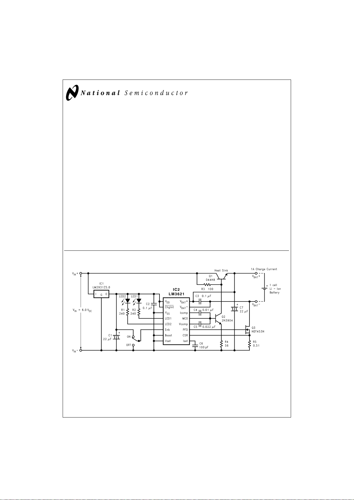
Typical Application
DS100107-7
1A, 4.1V CVCC Linear Charger for Graphite Anode Lithium-Ion Battery
March 1998
LM3621 Single Cell Lithium-Ion Battery Charger Controller
© 1998 National Semiconductor Corporation DS100107 www.national.com
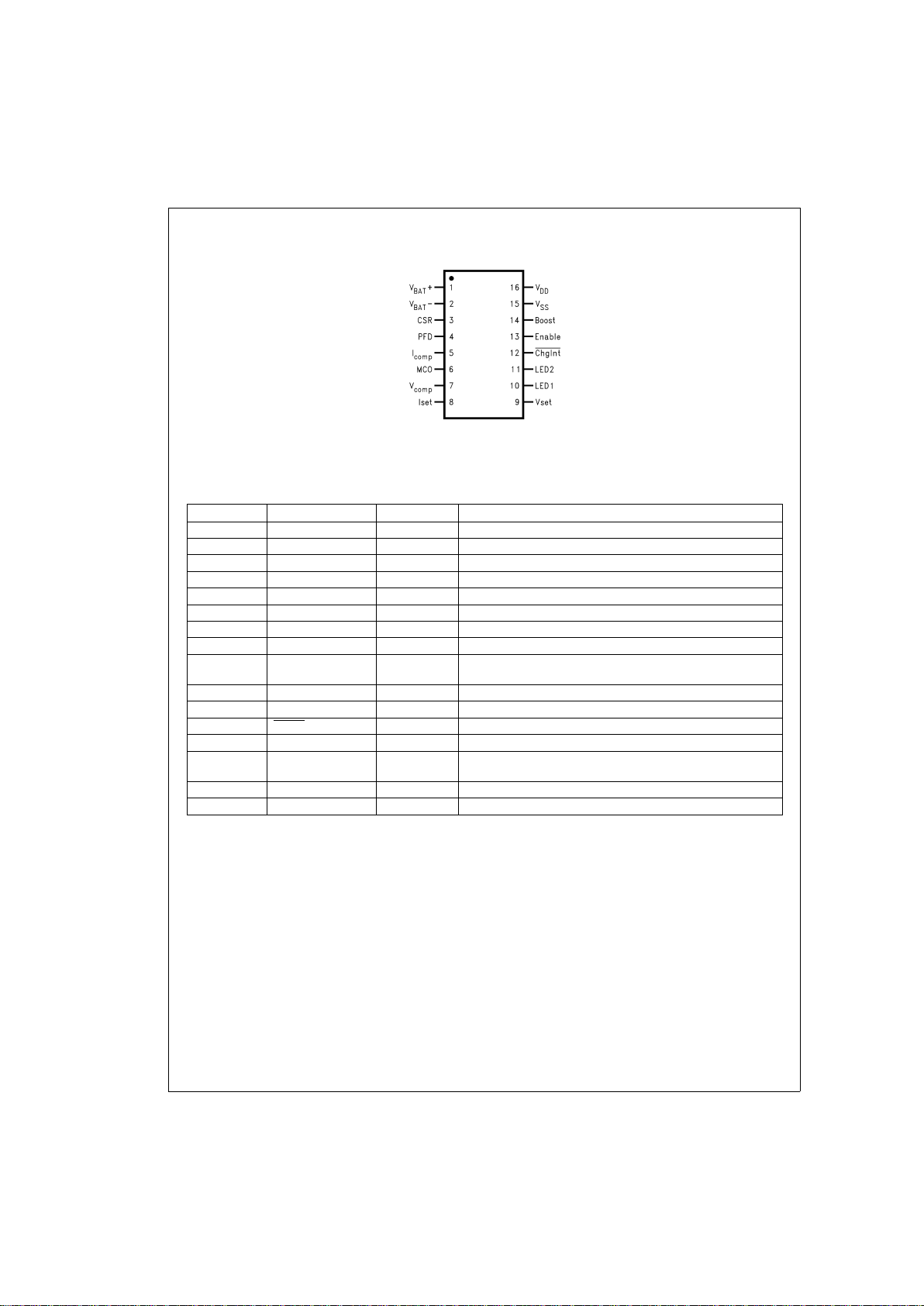
Connection Diagram
Pin Description
Pin No. Symbol I/O Description
1V
BAT
+ I Battery pack high side sense input.
2V
BAT
− I Battery pack low side sense input.
3 CSR I Current Sense Resistor high side input.
4 PFD O Pass FET gate Drive output. (N-channel).
5I
COMP
I Compensation pin for current regulation loop.
6 MCO O Modulation Control Output- analog control signal output
7V
COMP
I Compensation pin for voltage regulation loop.
8I
SET
I Charge current adjust input pin (see application section).
9V
SET
I Charge termination voltage control input (V
SET
=
HI for 4.2V or
V
SET
=
LO for 4.1V).
10 LED1 O LED driver #1 output (open drain).
11 LED2 O LED driver #2 output (open drain).
12 ChgInt
I Charge current interrupt (active LO).
13 Enable I Enable charge cycle control.
14 Boost I Maximum output current boost control (max output current
increased by 80%).
15 V
SS
S IC common.
16 V
DD
S IC power supply.
16-Lead SOIC
DS100107-18
Top View
Order Number LM3621M or LM3621M-3.0
NSC Package Number M16A
www.national.com 2
Absolute Maximum Ratings (Note 1)
If Military/Aerospace specified devices are required,
please contact the National Semiconductor Sales Office/
Distributors for availability and specifications.
Supply Voltage, V
DD
6.0V
All pins −0.3 V ≤ V ≤ V
DD
+0.3V
Power Dissipation 100 mV
ESD Susceptibility (Note 2) 2kV
Junction Temperature 150˚C
Storage Temperature −65˚C to +150˚C
Lead Temperature,
soldering
Vapor Phase (60 sec) +215˚C
Infrared (15 sec) +220˚C
Operating Ratings
Ambient Temperature Range 0˚C ≤ TA≤ 70˚C
Supply Voltage Range (Note 3) 3.0V ≤ V
DD
≤ 5.5V
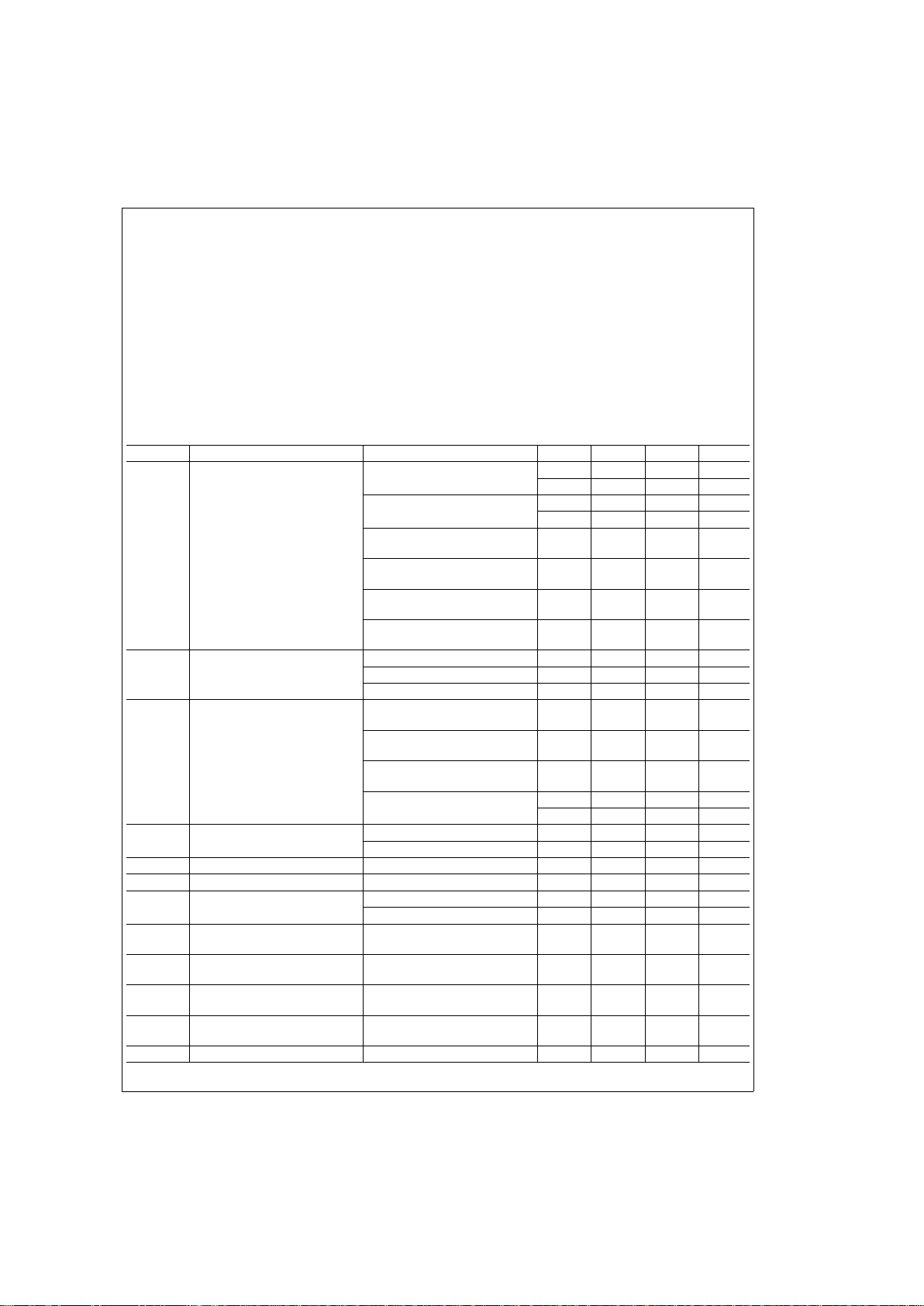
Electrical Characteristics
V
DD
=
4.2V unless otherwise specified. Specifications with standard type face are for T
A
=
25˚C, and those with boldface type
apply over full operating temperature range.
Symbol Parameter Conditions Min Typ Max Units
V
OUT
Battery Regulation Voltage (Note
4)
Charge termination voltage for
V
SET
=
HI
4.18 4.2 4.22 V
4.16 4.24 V
Charge termination voltage for
V
SET
=
LO
4.08 4.1 4.12 V
4.06 4.14 V
Battery conditioning (Hi-Z) charge
mode, LM3621M-3.0
2.95 3.1 3.25 V
Battery conditioning (Hi-Z) charge
mode, LM3621M
4.05 4.1 4.15 V
Monitor Mode float voltage for
V
SET
=
HI
4.05 4.09 4.13 V
Monitor Mode float voltage for
V
SET
=
LO
3.80 3.85 3.90 V
V
CSR
Charge Current Regulation
Voltage (Notes 5, 16)
Fast Charge Mode 0.475 0.5 0.525 V
Conditioning (Hi-Z) Charge Mode 0.04 0.05 0.06 V
Boost Mode 0.855 0.9 0.945 V
V
BAT
-Det Battery Voltage Detection
Threshold (Note 6)
Overvoltage Fault Threshold for
V
SET
=
HI
4.28 4.40 4.50 V
Overvoltage Fault Threshold for
V
SET
=
LO
4.18 4.30 4.40 V
Battery Resistance Free Voltage
Threshold
3.55 3.65 3.75 V
Conditioning (Hi-Z) Charge Mode
Threshold
2.45 2.55 2.65 V
2.40 2.70 V
V
CSR
-Det Charge Current Voltage Detection
Threshold (Notes 7, 16)
End of charge threshold 40 mV
Over Current Fault Threshold 0.95 1 1.05 V
IQ Quiescent Current Standby Mode with I
OUT
=
0mA 3 5 mA
I
OUT
MCO Output Source Current V
MCO
=
1.0V 20 mA
V
MCO
Maximum MCO Output Voltage I
OUT
=
1 mA, V
DD
=
5.5V 4.9 V
I
OUT
=
1 mA, V
DD
=
3.0V 2.9 V
GM-V V-Reg Loop Error Amp
Transconductance
0.1 mA/V
I
SLEW
-V V-Reg Loop Error Amp Slew
Current
100 µA
GM-I I-Reg Loop Error Amp
Transconductance
1 mA/V
I
SLEW
-I I-Reg Loop Error Amp Slew
Current
200 µA
T
HR
1 Hour Timer 55 60 65 min
3 www.national.com
Electrical Characteristics (Continued)
V
DD
=
4.2V unless otherwise specified. Specifications with standard type face are for T
A
=
25˚C, and those with boldface type
apply over full operating temperature range.
Symbol Parameter Conditions Min Typ Max Units
I
LKG
-0 Battery Load Current (Note 8) V
DD
=
0V 1 10 µA
I
LKG
-MM Battery Load Current (Note 9) Monitor Mode 1 10 µA
V
BSD
Maximum Allowed Battery SelfDischarge(Note 10)
V
SET
=
HI 70 110 150 mV
V
SET
=
LO 220 260 300 mV
G
CSR
Fast Charge Current Regulation
Adjustment Transfer Ratio (Notes
11, 12)
V
ISET
=
0.5V 0.90 0.93 0.96 V/V
I
LED
LED1 & LED2 Driver Sink Current V
LED1
=
V
LED2
=
1.5V 20 mA
V
SUV
Start Up Voltage (Note 13) 3.4 V
V
UVR
Under Voltage Reset (Note 14) 2.2 V
V
PFD
-MAX Maximum PFD Output Drive no DC load on PFD VDD−0.2 V
V
PFD
-MIN Minimum PFD Output Drive no DC load on PFD VSS+0.1 V
V
IL
Logic Input Low (Note 15) 0.5 V
V
IH
Logic Input High (Note 15) VDD−0.5 V
I
DIG
Digital Input Leakage Current
(Note 15)
−1 1 µA
Note 1: Absolute Maximum Ratings indicates limits beyond which damage to the device may occur. Operating ratings indicate conditions for which the device is intended to be functional, but device parameter specifications may not be guaranteed under these conditions. For guaranteed specifications and test conditions, see
the Electrical Characteristics.
Note 2: ESD rating is based on the human body model, 100 pF discharged through 1.5 kΩ.
Note 3: LM3621 requires a minimum V
DD
of 3.4V to start-up. After start-up, the operating range is 3.0V to 5.5V.
Note 4: V
OUT
is measured between V
BAT
+ and CSR.
Note 5: V
CSR
is measured between CSR and VSS(across the current sense resistor).
Note 6: V
BAT
-Det is measured between V
BAT
+ and V
BAT
−.
Note 7: V
CSR
-Det is measured between CSR and VSS(across the current sense resistor).
Note 8: This is the current drawn from the battery by the LM3621 when V
DD
=
0V.
Note 9: This is the current drawn from the battery by the LM3621 when the charger is in Monitor Mode.
Note 10: This is the maximum battery voltage droop that is allowed before the charger initiates a fast charge mode to refresh the battery to its full charge capacity.
Note 11: The current regulation and detection levels can be set by applying a dc voltage adjusting between 0.1V to 1V to the I
SET
pin without changing the value
of the current sense resistor. To ensure proper operation, if the default current regulation and detection values are desired, then a capacitor of at least 100 pF should
be connected from I
SET
to VSS(GND).
Note 12: Transfer ratio of V
CSR/VISET
to adjust the fast charge current regulation level. See application section.
Note 13: Minimum V
DD
supply voltage required at start-up.
Note 14: The LM3621 goes to a shutdown or reset state during “brown out” (i.e., when V
DD
<
V
UVR
)
Note 15: Digital inputs are Enable, Boost, Chgint and V
SET
. To ensure proper operation, never allow any unused input pin to be left open.
Note 16: No external voltage applied to I
set
pin; a 100 pF capacitor is connected across I
set
and VSS.
Definition of Terms
V
OUT
: Voltage measured between V
BAT
+ and CSR.
V
CSR
: Charging current sense voltage measured between
CSR and V
SS
(Gnd).
V
BATTERY
: Battery terminal voltage measured between
V
BAT
+ and V
BAT
−.
ESR: The equivalent series resistance of a battery.The ESR
is the purely resistive component of a battery’s impedance.
Its value is usually determined by the battery construction.
RFV:The RFV (resistance free voltage, often called the float
voltage) is the open circuit terminal voltage of a battery
which is free from the ESR voltage drop error.
VI
SET
: External voltage applied to I
SET
pin, measured be-
tween I
SET
and VSS, to override the default value of V
CSR
.
www.national.com 4
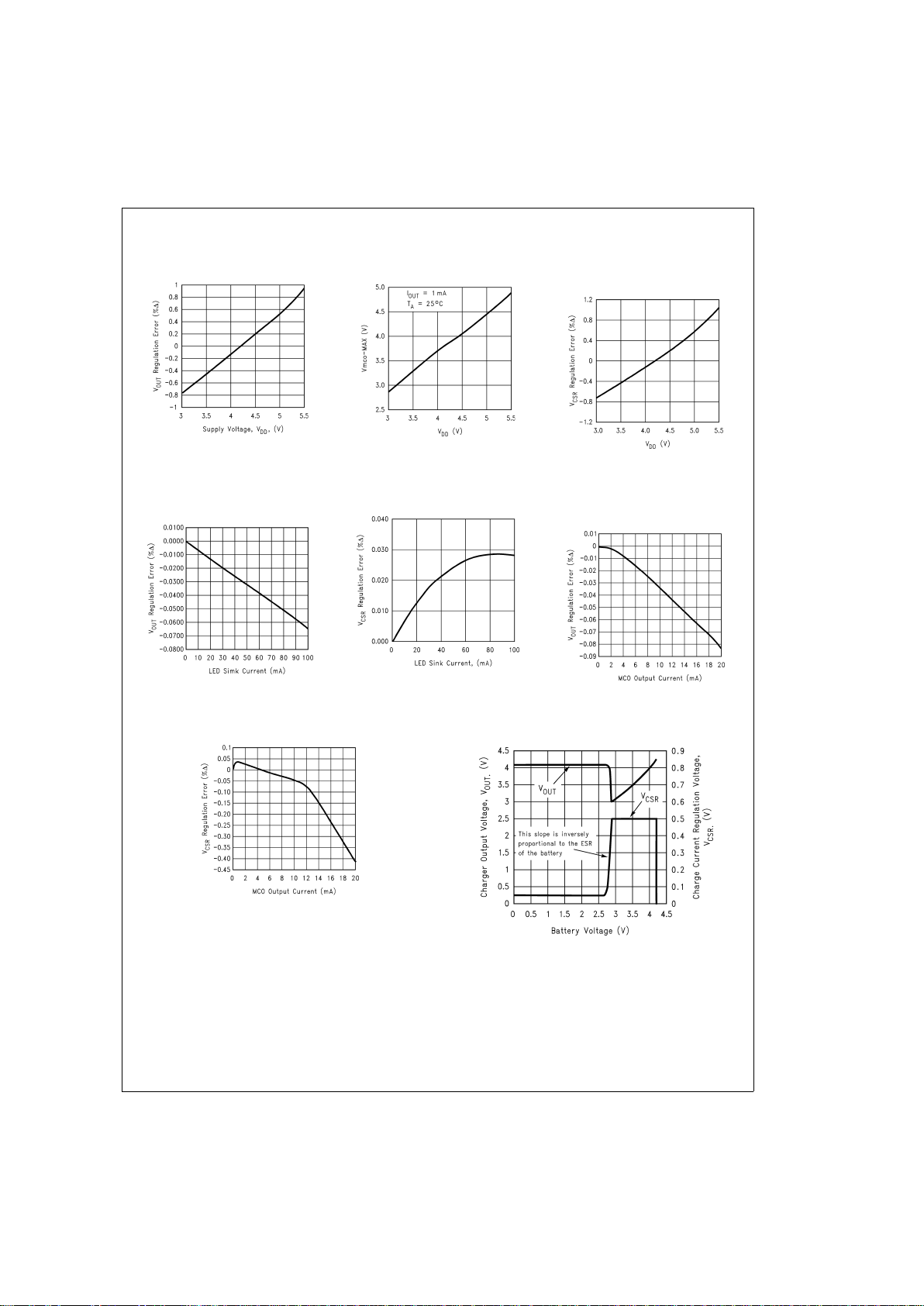
Typical Performance Characteristics Unless otherwise specified, T
A
=
25˚C)
Charge Termination Voltage
Change vs V
DD
DS100107-10
Maximum MCO Output Voltage vs
V
DD
DS100107-17
Fast Charge Current Regulation
Voltage vs V
DD
DS100107-15
Charge Termination Voltage
Regulation vs LED1 or LED2 Sink
Current
DS100107-19
Fast Charge Current Regulation vs
LED1 or LED2 Sink Current
DS100107-20
Charge Termination Voltage
Regulation vs MCO Output Current,
I
OUT
DS100107-22
Fast Charge Current Regulation vs MCO Output
Current, I
OUT
DS100107-21
Charger Output Voltage Current Regulation Voltage vs
Battery Resistance Free Voltage
DS100107-14
5 www.national.com
 Loading...