NSC LM346J Datasheet
LM146/LM346
Programmable Quad Operational Amplifiers
General Description
The LM146 series of quad op amps consists of four independent, high gain, internally compensated, low power, programmable amplifiers. Two external resistors (R
SET
) allow
the user to program the gain bandwidth product, slew rate,
supply current, input bias current, input offset current and input noise. For example, the user can trade-off supply current
for bandwidth or optimize noise figure for a given source resistance. In a similar way, other amplifier characteristics can
be tailored to the application. Except for the two programming pins at the end of the package, the LM146 pin-out is
the same as the LM124 and LM148.
Features
(I
SET
=10 µA)
n Programmable electrical characteristics
n Battery-powered operation
n Low supply current: 350 µA/amplifier
n Guaranteed gain bandwidth product: 0.8 MHz min
n Large DC voltage gain: 120 dB
n Low noise voltage: 28
n Wide power supply range:±1.5V to±22V
n Class AB output stage–no crossover distortion
n Ideal pin out for Biquad active filters
n Input bias currents are temperature compensated
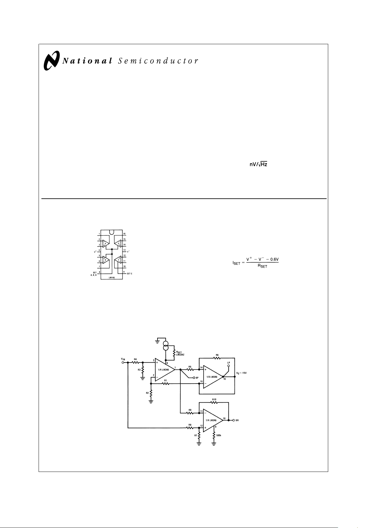
Connection Diagram
PROGRAMMING EQUATIONS
Total Supply Current = 1.4 mA (I
SET
/10 µA)
Gain Bandwidth Product = 1 MHz (I
SET
/10 µA)
Slew Rate = 0.4V/µs (I
SET
/10 µA)
Input Bias Current . 50 nA (I
SET
/10 µA)
I
SET
= Current into pin 8, pin 9 (see schematic-diagram)
Capacitorless Active Filters (Basic Circuit)
Dual-In-Line Package
DS005654-1
Top View
Order Number LM146J, LM146J/883,
LM346M,LM346MX or LM346N
See NS Package Number
J16A, M16A or N16A
DS005654-16
August 2000
LM146/LM346 Programmable Quad Operational Amplifiers
© 2000 National Semiconductor Corporation DS005654 www.national.com
Absolute Maximum Ratings (Notes 1, 5)
If Military/Aerospace specified devices are required, please contact the National Semiconductor Sales Office/
Distributors for availability and specifications.
LM146 LM346
Supply Voltage
±
22V
±
18V
Differential Input Voltage (Note 1)
±
30V
±
30V
CM Input Voltage (Note 1)
±
15V
±
15V
Power Dissipation (Note 2) 900 mW 500 mW
Output Short-Circuit Duration (Note 3) Continuous Continuous
Operating Temperature Range −55˚C to +125˚C 0˚C to +70˚C
Maximum Junction Temperature 150˚C 100˚C
Storage Temperature Range −65˚C to +150˚C −65˚C to +150˚C
Lead Temperature (Soldering, 10 seconds) 260˚C 260˚C
Thermal Resistance (θ
jA
), (Note 2)
Cavity DIP (J) Pd 900 mW 900 mW
θ
jA
100˚C/W 100˚C/W
Small Outline (M) θ
jA
115˚C/W
Molded DIP (N) Pd 500 mW
θ
jA
90˚C/W
Soldering Information
Dual-In-Line Package
Soldering (10 seconds) +260˚C +260˚C
Small Outline Package
Vapor Phase (60 seconds) +215˚C +215˚C
Infrared (15 seconds) +220˚C +220˚C
SeeAN-450“SurfaceMountingMethodsandTheir Effect on Product Reliability” for other methods of soldering surface mount devices.
ESD rating is to be determined.
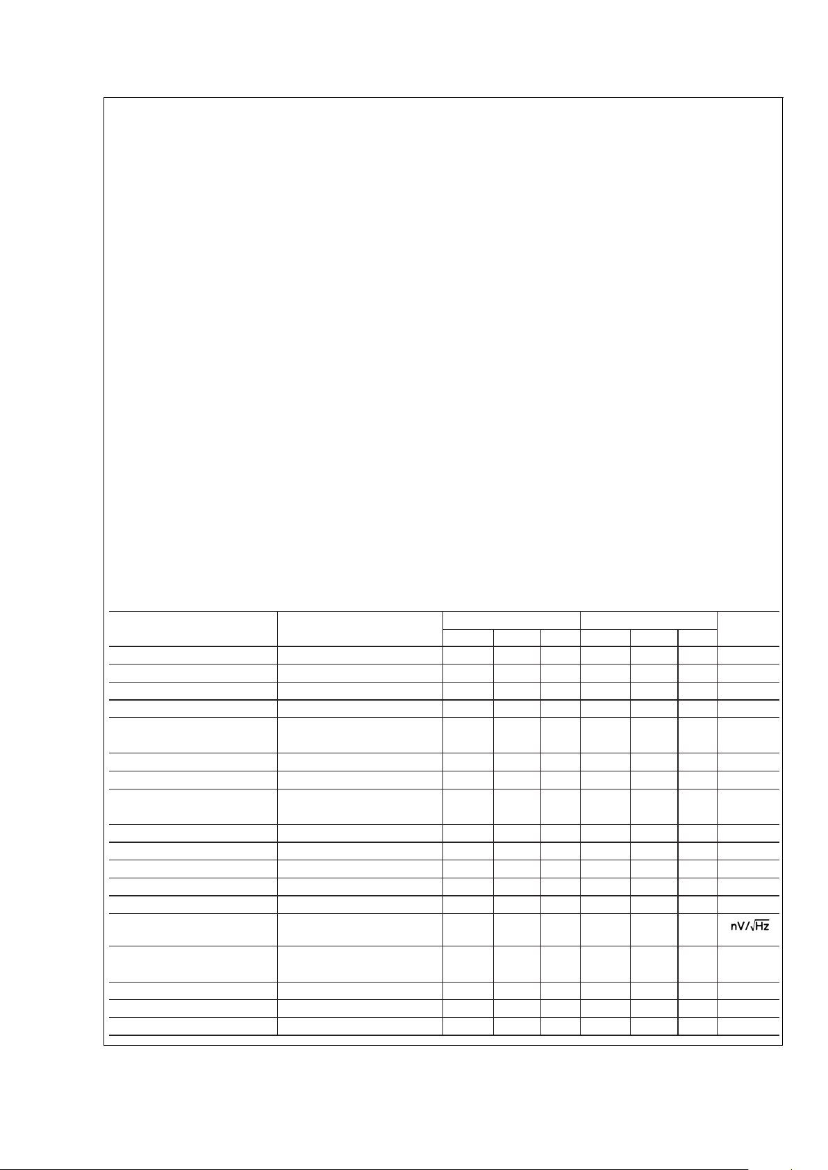
DC Electrical Characteristics
(VS=±15V, I
SET
=10 µA), (Note 4)
Parameter Conditions LM146 LM346 Units
Min Typ Max Min Typ Max
Input Offset Voltage V
CM
=0V, RS≤50Ω,TA=25˚C 0.5 5 0.5 6 mV
Input Offset Current V
CM
=0V, TA=25˚C 2 20 2 100 nA
Input Bias Current V
CM
=0V, TA=25˚C 50 100 50 250 nA
Supply Current (4 Op Amps) T
A
=25˚C 1.4 2.0 1.4 2.5 mA
Large Signal Voltage Gain R
L
=10 kΩ, ∆V
OUT
=±10V, 100 1000 50 1000 V/mV
T
A
=25˚C
Input CM Range T
A
=25˚C
±
13.5
±
14
±
13.5
±
14 V
CM Rejection Ratio R
S
≤10 kΩ,TA=25˚C 80 100 70 100 dB
Power Supply Rejection Ratio R
S
≤10 kΩ,TA=25˚C, 80 100 74 100 dB
V
S
=±5to±15V
Output Voltage Swing R
L
≥10 kΩ,TA=25˚C
±
12
±
14
±
12
±
14 V
Short-Circuit T
A
=25˚C 5 20 35 5 20 35 mA
Gain Bandwidth Product T
A
=25˚C 0.8 1.2 0.5 1.2 MHz
Phase Margin T
A
=25˚C 60 60 Deg
Slew Rate T
A
=25˚C 0.4 0.4 V/µs
Input Noise Voltage f=1 kHz, T
A
=25˚C 28 28
Channel Separation RL=10 kΩ, ∆V
OUT
=0V to 120 120 dB
±
12V, TA=25˚C
Input Resistance T
A
=25˚C 1.0 1.0 MΩ
Input Capacitance T
A
=25˚C 2.0 2.0 pF
Input Offset Voltage V
CM
=0V, RS≤50Ω 0.5 6 0.5 7.5 mV
LM146/LM346
www.national.com 2
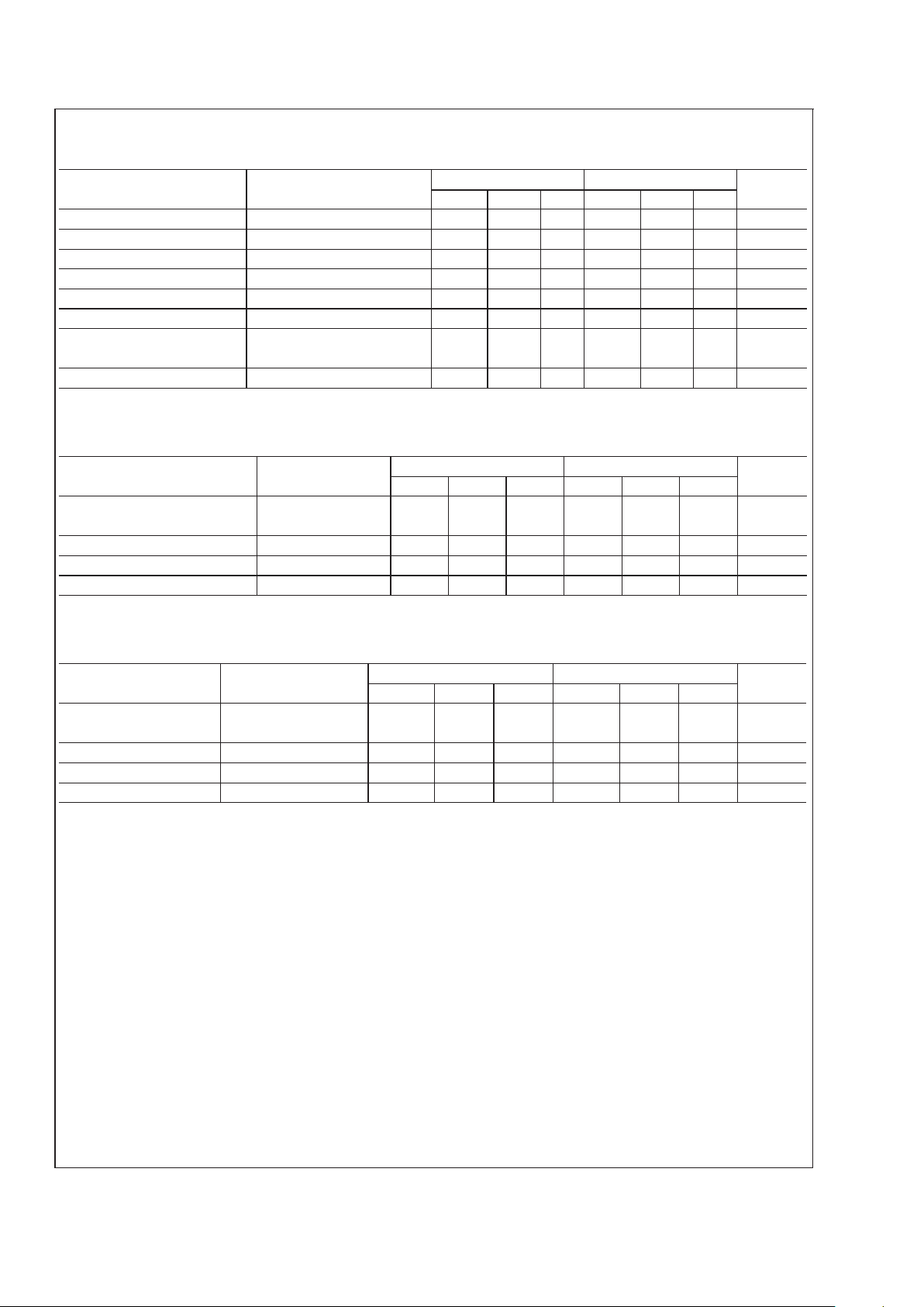
DC Electrical Characteristics (Continued)
(VS=±15V, I
SET
=10 µA), (Note 4)
Parameter Conditions LM146 LM346 Units
Min Typ Max Min Typ Max
Input Offset Current V
CM
=0V 2 25 2 100 nA
Input Bias Current V
CM
=0V 50 100 50 250 nA
Supply Current (4 Op Amps) 1.7 2.2 1.7 2.5 mA
Large Signal Voltage Gain R
L
=10 kΩ, ∆V
OUT
=±10V 50 1000 25 1000 V/mV
Input CM Range
±
13.5
±
14
±
13.5
±
14 V
CM Rejection Ratio R
S
≤50Ω 70 100 70 100 dB
Power Supply Rejection Ratio R
S
≤50Ω, 76 100 74 100 dB
V
S
=±5V to±15V
Output Voltage Swing R
L
≥10 kΩ
±
12
±
14
±
12
±
14 V
DC Electrical Characteristic
(VS=±15V, I
SET
=10 µA)
Parameter Conditions LM146 LM346 Units
Min Typ Max Min Typ Max
Input Offset Voltage V
CM
=0V, RS≤50Ω, 0.5 5 0.5 7 mV
T
A
=25˚C
Input Bias Current V
CM
=0V, TA=25˚C 7.5 20 7.5 100 nA
Supply Current (4 Op Amps) T
A
=25˚C 140 250 140 300 µA
Gain Bandwidth Product T
A
=25˚C 80 100 50 100 kHz
DC Electrical Characteristics
(VS=±1.5V, I
SET
=10 µA)
Parameter Conditions LM146 LM346 Units
Min Typ Max Min Typ Max
Input Offset Voltage V
CM
=0V, RS≤50Ω, 0.5 5 0.5 7 mV
T
A
=25˚C
Input CM Range T
A
=25˚C
±
0.7
±
0.7 V
CM Rejection Ratio R
S
≤50Ω,TA=25˚C 80 80 dB
Output Voltage Swing R
L
≥10 kΩ,TA=25˚C
±
0.6
±
0.6 V
Note 1: For supply voltages less than±15V, the absolute maximum input voltage is equal to the supply voltage.
Note 2: The maximum power dissipation for these devices must be derated at elevated temperatures and is dictated by T
jMAX
, θjA, and the ambient temperature,
T
A
. The maximum available power dissipation at any temperature is Pd=(T
jMAX-TA
)/θjAor the 25˚C P
dMAX
, whichever is less.
Note 3: Any of the amplifier outputs can be shorted to ground indefinitely; however, more than one should not be simultaneously shorted as the maximum junction
temperature will be exceeded.
Note 4: These specifications apply over the absolute maximum operating temperature range unless otherwise noted.
Note 5: Refer to RETS146X for LM146J military specifications.
LM146/LM346
www.national.com3
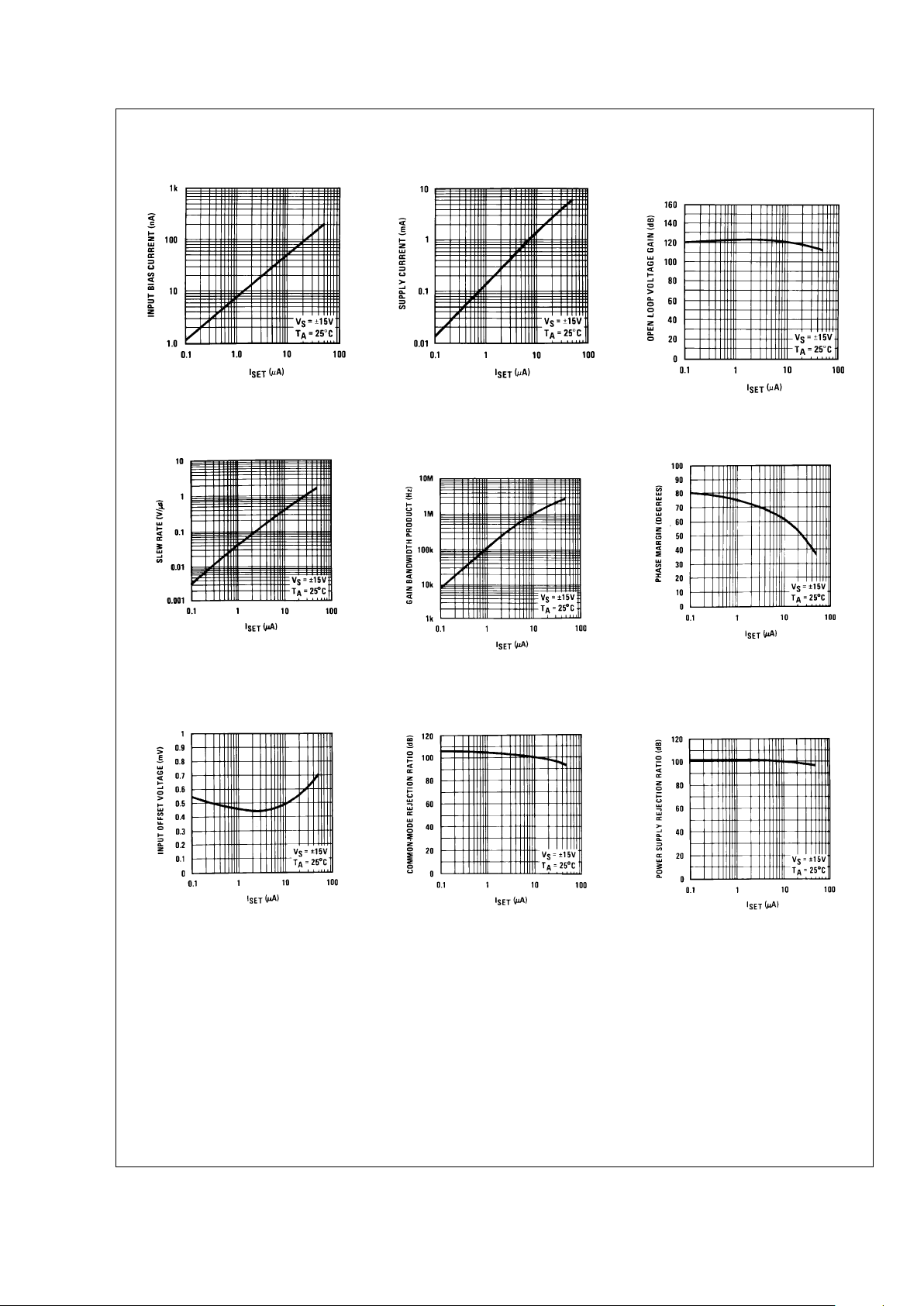
Typical Performance Characteristics
Input Bias Current vs I
SET
DS005654-44
Supply Current vs I
SET
DS005654-45
Open Loop Voltage Gain
vs I
SET
DS005654-46
Slew Rate vs I
SET
DS005654-47
Gain Bandwidth Product
vs I
SET
DS005654-48
Phase Margin vs I
SET
DS005654-49
Input Offset Voltage
vs I
SET
DS005654-50
Common-Mode Rejection
Ratio vs I
SET
DS005654-51
Power Supply Rejection
Ratio vs I
SET
DS005654-52
LM146/LM346
www.national.com 4
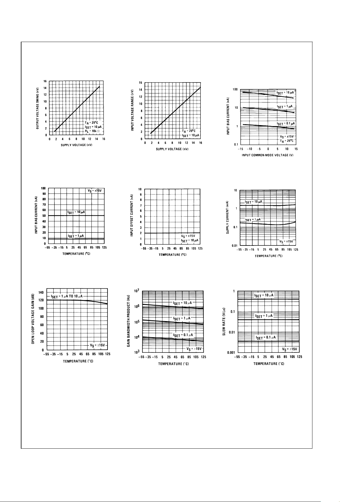
Typical Performance Characteristics (Continued)
Open Voltage Swing vs
Supply Voltage
DS005654-53
Input Voltage Range vs
Supply Voltage
DS005654-54
Input Bias Current vs
Input Common-Mode
Voltage
DS005654-55
Input Bias Current vs
Temperature
DS005654-56
Input Offset Current vs
Temperature
DS005654-57
Supply Current vs
Temperature
DS005654-58
Open Loop Voltage Gain
vs Temperature
DS005654-20
Gain Bandwidth Product
vs Temperature
DS005654-21
Slew Rate vs
Temperature
DS005654-22
LM146/LM346
www.national.com5
 Loading...