

NSC LM3460M5-1.5, LM3460M5-1.2, LM3460M5X-1.5 Datasheet
May 1999
LM3460-1.2, -1.5
Precision Controller for GTLp and GTL Bus Termination
LM3460-1.2, -1.5 Precision Controller for GTLp and GTL Bus Termination
General Description
The LM3460 is a monolithic integrated circuit designed for
precision control of GTLplus and GTL Bus termination. This
controller is available in a tiny SOT23-5 package, and includes an internally compensated op amp, a bandgap reference, an NPN output transistor,andvoltage setting resistors.
A trimmed precision bandgap voltage reference utilizes temperature drift curvature correction for excellent voltage stability over the operating range. The precision output control enables the termination voltage to maintain tight regulation,
despite fast switching requirements on the bus.
The LM3460 controller is designed to be used with a high
>
current (
rent needed for the bus termination. The wide bandwidth of
the feedback loop provides excellent transient response,
and greatly reduces the output capacitance required, thus
reducing cost and board space requirements.
7A) NPN pass transistor to provide the high cur-
Features
n Precision output (1%)
n Output voltage can be adjusted
n Extremely fast transient response in GTLp and GTL bus
termination
n Tiny SOT23-5 package
n Output voltage capability for GTL or GTLp
n Low temperature coefficient
Applications
n GTL bus termination (1.2V output 7A)
n GTLp bus termination (1.5V output 7A)
n Adjustable high-current linear regulator
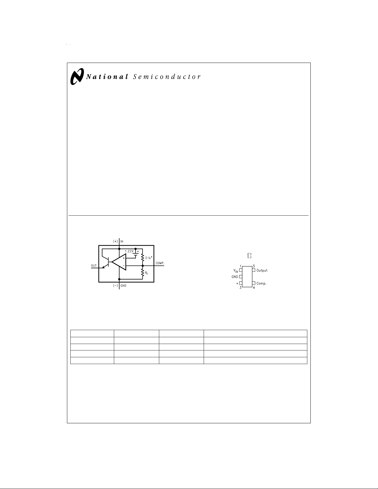
Connection Diagram and Package Information
*
This resistor is not used on the LM3460-1.2.
LM3460 Functional Diagram
DS012603-1
*
No internal connection, but should be soldered to PC board for best heat
transfer.
5-Lead Outline Package (M5)
Actual Size
DS012603-2
DS012603-3
Top View
See NS package Number MA05B
Ordering Information
Voltage Order Number Package Marking Supplied As
1.5 LM3460M5-1.5 D06A 250 Unit Increments on Tape and Reel
1.5 LM3460M5X-1.5 D06A 3k Unit Increments on Tape and Reel
1.2 LM3460M5-1.2 D09A 250 Unit Increments on Tape and Reel
1.2 LM3460M5X-1.5 D09A 3k Unit Increments on Tape and Reel
MARKING CODE: The first letter ″D″ identifies the part as a Driver, and the next two numbers define the voltage for the part. The fourth letter indicates the
grade, with ″A″ designating the prime grade of product.
AVAILABILITY: The SOT23-5 package is only available in quantity of 250 on tape and reel (designated by the letters ″M5″ in the part number), or in quantity
of 3000 on tape and reel (indicated by the letters ″M5X″ in the part number).
© 1999 National Semiconductor Corporation DS012603 www.national.com
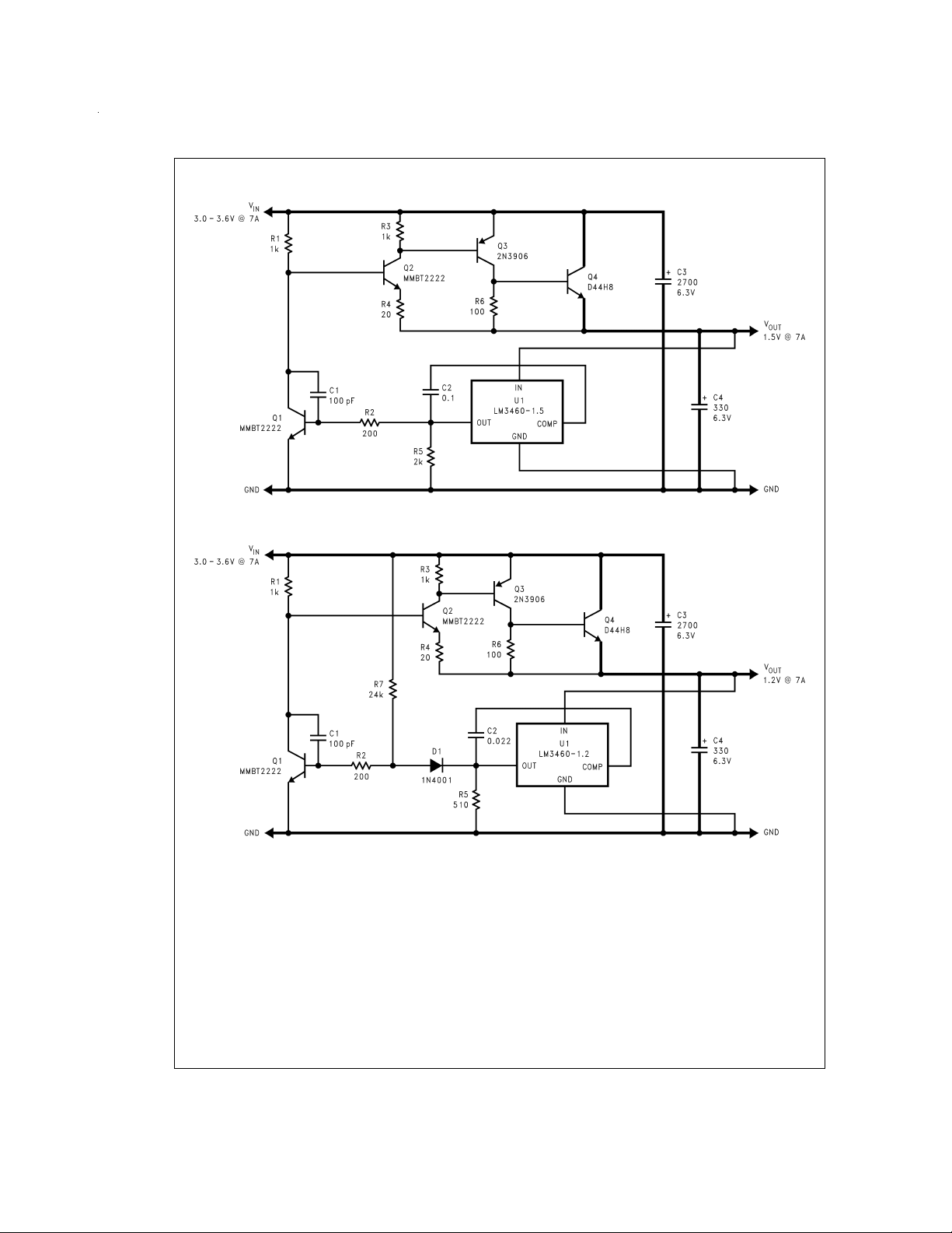
Typical Applications
FIGURE 1. 1.5V Typical Application (See Application Information Section)
DS012603-4
FIGURE 2. 1.2V Typical Application (See Application Information Section)
www.national.com 2
DS012603-5
Absolute Maximum Ratings (Note 1)
If Military/Aerospace specified devices are required,
please contact the National Semiconductor Sales Office/
Distributors for availability and specifications.
Input Voltage V
IN
Output Current 20 mA
Junction Temperature 150˚C
Storage Temperature −65˚C to +150˚C
Lead Temperature
Vapor Phase (60 sec.)
Infared (15 sec.)
20V
+215˚C
+220˚C
Power Dissipation (T
(Note 2) 300 mW
ESD Susceptibility (Note 3)
Human Body Model 1500V
See AN-450 ″Surface Mounting Methods and Their Effect
on Product Reliability″ for methods on soldering surface
mount devices.
Operating Ratings (Note 1), (Note 2)
Ambient Temperature Range 0˚C ≤ T
Output Current 1 mA
=
25˚C)
A
≤ +70˚C
A
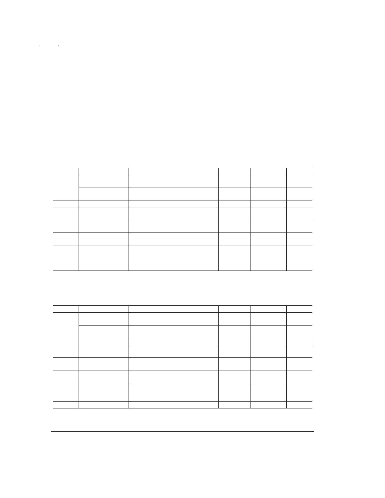
Electrical Characteristics
LM3460-1.5
Specifications with standard type face are for T
Range. Unless otherwise specified, (+)IN=V
Symbol Parameter Conditions Typ (Note 4) Limit (Note 5) Units
V
REG
I
q
G
m
V
SAT
I
L
R
F
Regulated Voltage I
Regulated Voltage
Tolerance
Quiescent Current I
Transconductance
/ ∆V
∆I
OUT
REG
Output Saturation
Voltage(Note 6)
Output Leakage
Current
Internal Feedback
Resistor (See
OUT
I
OUT
OUT
20µA ≤ I
V
OUT
V
IN
I
OUT
V
IN
V
OUT
Functional Diagram)
E
n
Output Noise Voltage I
OUT
=
25˚C, and those with boldface type apply over full Operating Temperature
J
REG,VOUT
=
1 mA 1.5 1.515/ 1.530
=
200 mV
1.485/1.470
=
1mA
=
1 mA 85 125/150 µA (max)
≤ 1mA
=
=
=
OUT
=
500 mV
V
REG
1mA
V
REG
=
0V
+ 100 mV
− 100 mV
3.3 1/0.5
0.8 0.95 V (max)
0.1 0.5/1.0 µA (max)
7.1
=
1 mA, 10 Hz ≤ f ≤ 10kHz 50 µV (rms)
±1/±
8.9
5.3
2
V (max)
V (min)
%
mA/mV
kΩ(max)
kΩ(min)
(max)
(min)
Electrical Characteristics
LM3460-1.2
Specifications with standard type face are for T
Range. Unless otherwise specified, (+)IN=V
Symbol Parameter Conditions Typ (Note 4) Limit (Note 5) Units
V
REG
I
q
G
m
V
SAT
I
L
R
F
Regulated Voltage I
Regulated Voltage
Tolerance
Quiescent Current I
Transconductance
/ ∆V
∆I
OUT
REG
Output Saturation
Voltage(Note 6)
Output Leakage
Current
Internal Feedback
Resistor (See
OUT
I
OUT
OUT
20µA ≤ I
V
OUT
V
IN
I
OUT
V
IN
V
OUT
Functional Diagram)
E
n
Output Noise Voltage I
OUT
=
25˚C, and those with boldface type apply over full Operating Temperature
J
REG,VOUT
=
1 mA 1.220 1.232/ 1.244
=
200 mV
1.208/1.196
=
1mA
=
1 mA 85 125/150 µA (max)
≤ 1mA
=
=
=
OUT
=
200 mV
V
REG
1mA
V
REG
=
0V
+ 100 mV
− 100 mV
3.3 1/0.5
0.8 0.95 V (max)
0.1 0.5/1.0 µA (max)
10
=
1 mA, 10 Hz ≤ f ≤ 10kHz 50 µV (rms)
±1/±
12.5
7.5
2
www.national.com3
V (max)
V (min)
%
mA/mV
kΩ(max)
kΩ(min)
(max)
(min)
 Loading...