

NSC LM342P-5.0, LM342P-15, LM342P-12 Datasheet
TL/H/10485
LM342 Series 3-Terminal Positive Regulators
June 1989
LM342 Series
3-Terminal Positive Regulators
General Description
The LM342-XX series of three-terminal regulators is available with several fixed output voltages, making them useful
in a wide range of applications. One of these is local on card
regulation, eliminating the distribution problems associated
with single point regulation. The voltages available allow
these regulators to be used in logic systems, instrumentation, HiFi, and other solid state electronic equipment. Although designed primarily as fixed voltage regulators these
devices can be used with external components to obtain
adjustable voltages and currents.
The LM342-XX series is available in the plastic TO-202
package. This package allows these regulators to deliver
over 0.25A if adequate heat sinking is provided. Current limiting is included to limit the peak output current to a safe
value. Safe area protection for the output transistor is provided to limit internal power dissipation. If internal power
dissipation becomes too high for the heat sinking provided,
the thermal shutdown circuit takes over, preventing the IC
from overheating.
Considerable effort was expended to make the LM342-XX
series of regulators easy to use and minimize the number of
external components. It is not necessary to bypass the
output, although this does improve transient response. Input
bypassing is needed only if the regulator is located far from
the filter capacitor of the power supply.
For output voltage other than 5V, 12V and 15V the LM117
series provides an output voltage range from 1.2V to 57V.
Features
Y
Output current in excess of 0.25A
Y
Internal thermal overload protection
Y
No external components required
Y
Output transistor safe area protection
Y
Internal short circuit current limit
Y
Available in plastic TO-202 package
Y
Special circuitry allows start-up even if output is pulled
to negative voltage (
g
supplies)
Voltage Range
LM342-5.0 5V
LM342-12 12V
LM342-15 15V
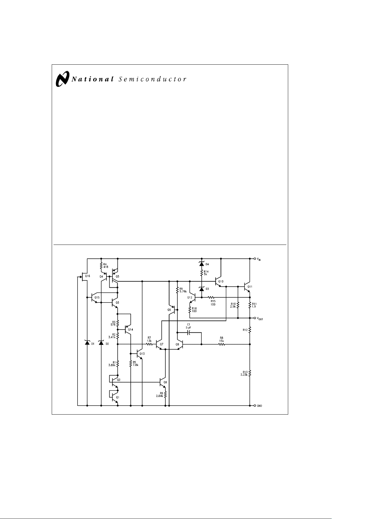
Schematic Diagram
TL/H/10485– 1
C
1995 National Semiconductor Corporation RRD-B30M115/Printed in U. S. A.
Absolute Maximum Ratings (Note 1)
If Military/Aerospace specified devices are required,
please contact the National Semiconductor Sales
Office/Distributors for availability and specifications.
Input Voltage
V
O
e
5V 30V
V
O
e
12V and 15V 35V
Internal Power Dissipation Internally Limited
Operating Temperature Range 0§Ctoa70§C
Maximum Junction Temperature 125
§
C
Storage Temperature Range
b
65§Ctoa150§C
Lead Temperature (Soldering, 10 sec.) 300§C
ESD Susceptibility TBD
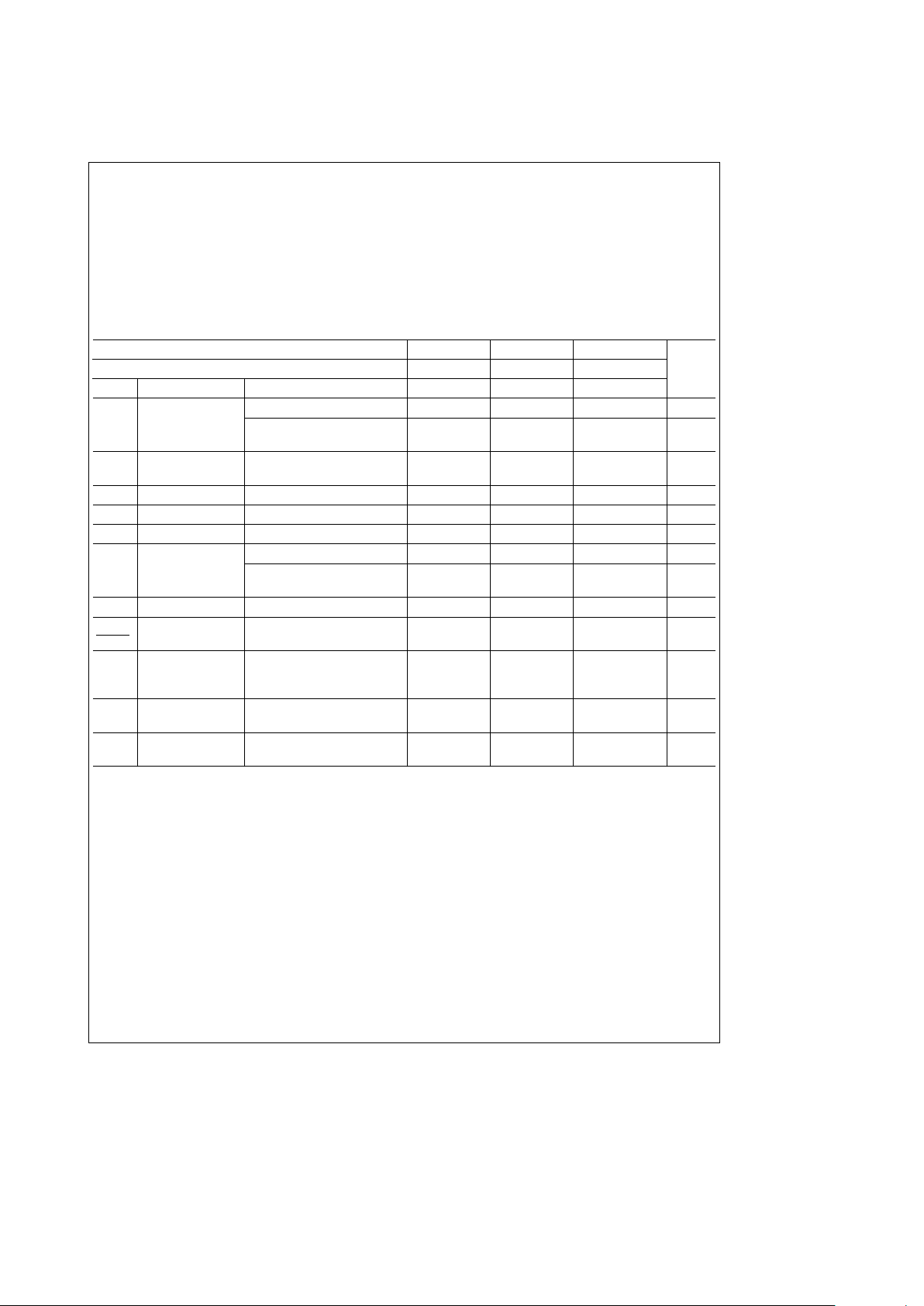
Electrical Characteristics T
A
e
0§Ctoa70§C, I
O
e
250 mA (Note 2) unless noted
Output Voltage 5V 12V 15V
Input Voltage (unless otherwise noted) 10V 19V 23V Units
Symbol Parameter Conditions Min Typ Max Min Typ Min Min Typ Max
V
O
Output Voltage T
J
e
25§C 4.8 5 5.2 11.5 12 12.5 14.4 15 15.6 V
(Note 3)
1mAsI
O
s
250 mA and 4.75 5.25 11.4 12.6 14.25 15.75 V
V
MIN
s
V
IN
s
V
MAX
(7.5sV
IN
s
20) (14.8sV
IN
s
27) (18sV
IN
s
30)
DVOLine Regulation T
J
e
25§C, I
O
e
250 mA 55 100 100 mV
(7.3
s
V
IN
s
25) (14.6sV
IN
s
30) (17.7sV
IN
s
30)
DVOLoad Regulation T
J
e
25§C,1mAsI
O
s
250 mA 50 120 150 mV
DVOLong Term Stability 20 48 60 mV/khrs
I
Q
Quiescent Current T
J
e
25§C666mA
DI
Q
Quiescent Current T
J
e
25§C,1mAsI
O
s
250 mA 0.5 0.5 0.5 mA
Change
T
J
e
25§C, V
MIN
s
V
IN
s
V
MAX
1.5 1.5 1.5 mA
(7.3
s
V
IN
s
25) (14.6sV
IN
s
30) (17.7sV
IN
s
30)
V
n
Output Noise Voltage T
J
e
25§C, fe10 Hz–10 kHz 40 96 120 mV
DV
IN
DV
OUT
Ripple Rejection fe120 Hz
50 64 44 56 42 56 dB
Input Voltage T
J
e
25§C, I
O
e
250 mA
Required to Maintain 7.3 14.6 17.7 V
Line Regulation
Thermal Resistance P Package
15 15 15
§
C/W
Junction to Case
Thermal Resistance P Package
80 80 80
§
C/W
Junction to Ambient
Note 1: Absolute Maximum Ratings indicate limits beyond which damage to the device may occur. Operating Ratings indicate conditions for which the device is
intended to be functional, but do not guarantee specific performance limits. For guaranteed specifications and test conditions, see the Electrical Characteristics.
Note 2: The electrical characteristics data represent pulse test conditions with junction temperatures as shown at the initiation of tests.
Note 3: The temperature coefficient of V
OUT
is typically within 0.01% VO/§C.
2
 Loading...