

NSC LM340LAZ-5.0, LM340LAZ-15, LM340LAZ-12, LM340LAH-12 Datasheet
February 1995
LM140L/LM340L Series 3-Terminal Positive Regulators
General Description
The LM140L series of three terminal positive regulators is
available with several fixed output voltages making them
useful in a wide range of applications. The LM140LA is an
improved version of the LM78LXX series with a tighter output voltage tolerance (specified over the full military temperature range), higher ripple rejection, better regulation and
lower quiescent current. The LM140LA regulators have
g
2% V
0.01%/mA load regulation. When used as a zener diode/re-
specification, 0.04%/V line regulation, and
OUT
sistor combination replacement, the LM140LA usually results in an effective output impedance improvement of two
orders of magnitude, and lower quiescent current. These
regulators can provide local on card regulation, eliminating
the distribution problems associated with single point regulation. The voltages available allow the LM140LA to be used
in logic systems, instrumentation, Hi-Fi, and other solid state
electronic equipment. Although designed primarily as fixed
voltage regulators, these devices can be used with external
components to obtain adjustable voltages and currents.
The LM140LA/LM340LA are available in the low profile
metal three lead TO-39 (H) and the LM340LA are also available in the plastic TO-92 (Z). With adequate heat sinking the
regulator can deliver 100 mA output current. Current limiting
is included to limit the peak output current to a safe value.
Safe area protection for the output transistor is provided to
limit internal power dissipation. If internal power dissipation
becomes too high for the heat sinking provided, the thermal
shut-down circuit takes over, preventing the IC from overheating.
For applications requiring other voltages, see LM117L Data
Sheet.
Features
Y
Line regulation of 0.04%/V
Y
Load regulation of 0.01%/mA
Y
Output voltage tolerances ofg2% at T
g
4% over the temperature range (LM140LA)
g
3% over the temperature range (LM340LA)
Y
Output current of 100 mA
Y
Internal thermal overload protection
Y
Output transistor safe area protection
Y
Internal short circuit current limit
Y
Available in metal TO-39 low profile package
e
j
25§C and
(LM140LA/LM340LA) and plastic TO-92 (LM340LA)
Output Voltage Options
LM140LA-5.0 5V LM340LA-5.0 5V
LM140LA-12 12V LM340LA-12 12V
LM140LA-15 15V LM340LA-15 15V
LM140L/LM340L Series 3-Terminal Positive Regulators
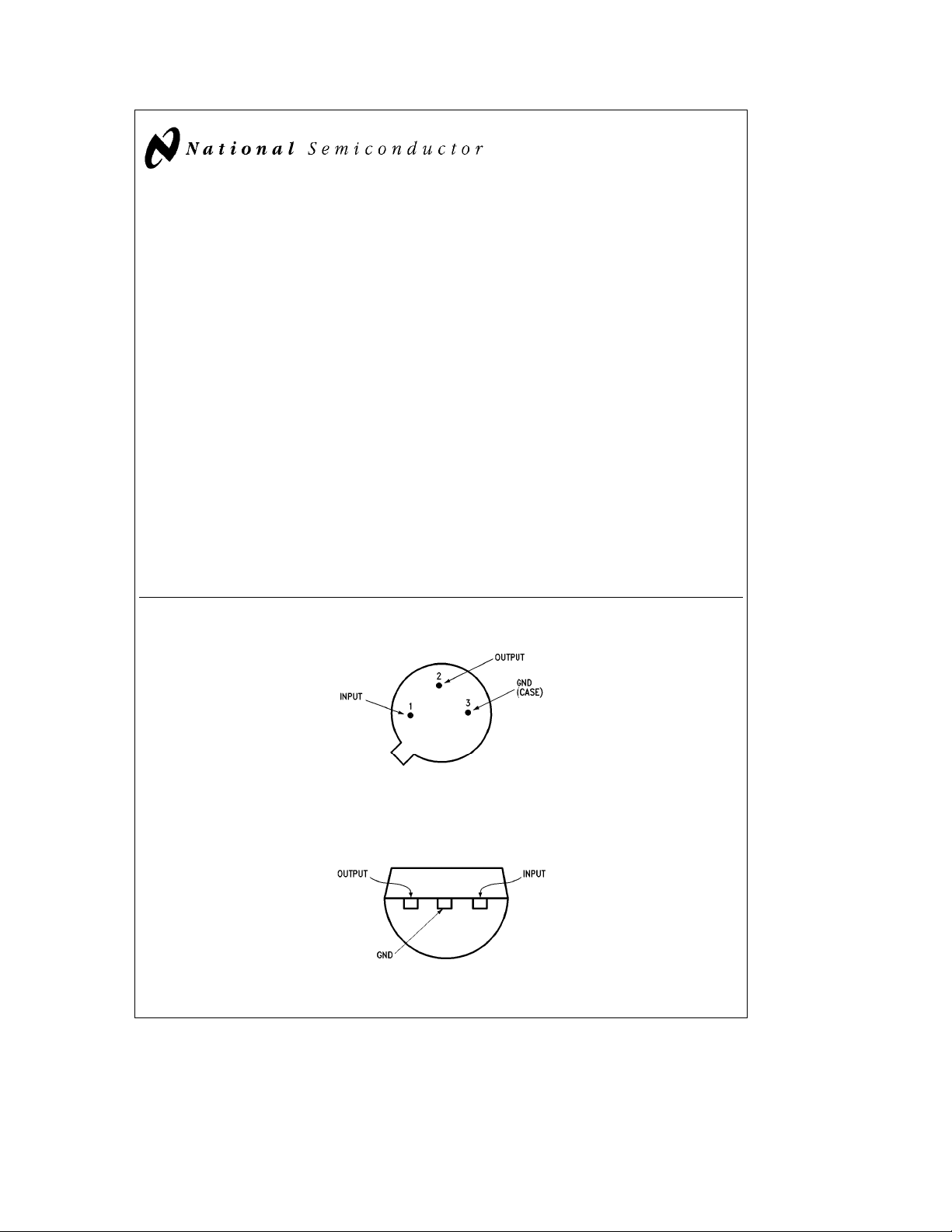
Connection Diagrams
TO-39 Metal Can Package (H)
Bottom View
Order Number LM140LAH-5.0, LM140LAH-5.0/883, LM140LAH-12,
LM140LAH-12/883, LM140LAH-15, LM140LAH-15/883, LM340LAH-5.0, LM340LAH-12 or LM340LAH-15
See NS Package Number H03A
TO-92 Plastic Package (Z)
Bottom View
Order Number LM340LAZ-5.0, LM340LAZ-12 or LM340LAZ-15
See NS Package Number Z03A
C
1995 National Semiconductor Corporation RRD-B30M115/Printed in U. S. A.
TL/H/7782
TL/H/7782– 2
TL/H/7782– 3
Absolute Maximum Ratings
If Military/Aerospace specified devices are required,
please contact the National Semiconductor Sales
Office/Distributors for availability and specifications.
(Note 4)
Input Voltage 35V
Internal Power Dissipation (Note 1) Internally Limited
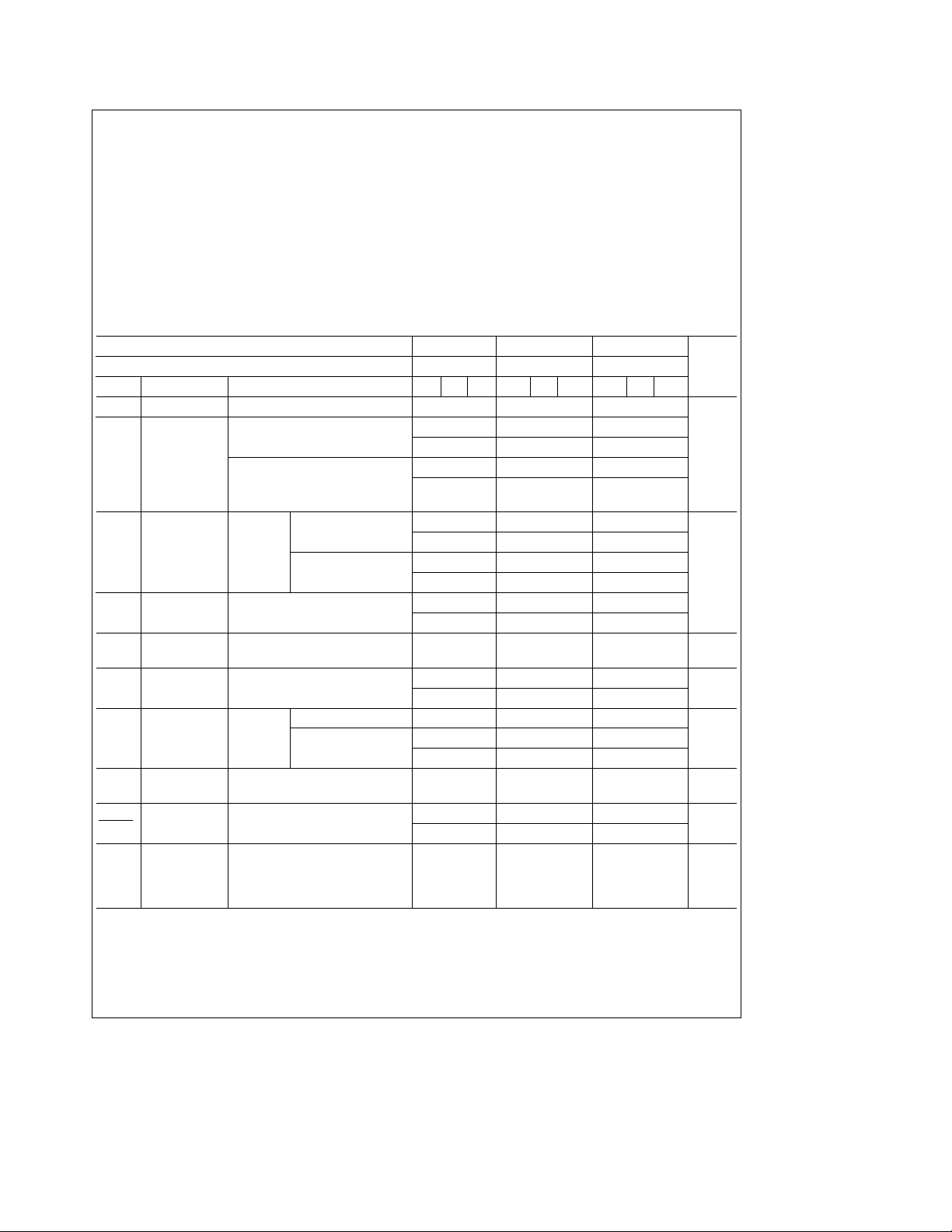
Electrical Characteristics
Test conditions unless otherwise specified. T
C
IN
e
0.33 mF, C
O
e
0.01 mF.
eb
55§Ctoa125§C (LM140LA), T
A
Output Voltage Option 5.0V 12V 15V
Input Voltage (unless otherwise noted) 10V 19V 23V Units
Symbol Parameter Conditions Min Typ Max Min Typ Max Min Typ Max
V
Output Voltage T
O
Output Voltage LM140LA I
Over Temp.
(Note 3)
DVOLine Regulation T
Load Regulation T
e
25§C 4.9 5 5.1 11.75 12 12.25 14.7 15 15.3
j
e1b
100 mA 4.8 5.2 11.5 12.5 14.4 15.6
O
LM340LA I
e
25§CI
j
e
25§CI
j
e1b
100 mA or 4.85 5.15 11.65 12.35 14.55 15.45
O
e1b
I
V
I
V
I
40 mA and
O
O
O
O
O
e
V
()V
IN
e
40 mA 18 30 30 65 37 70
e
()V
IN
e
100 mA 18 30 30 65 37 70
e
()V
IN
e1b
40 mA 5 20 10 40 12 50
e1b
100 mA
Long Term
Stability 1000 hrs
I
Quiescent T
O
Current T
DI
Quiescent T
Q
Current Change
V
Output Noise T
N
Voltage f
DV
IN
Ripple Rejection fe120 Hz, V
DV
OUT
e
25§C 3 4.5 3 4.5 3.1 4.5
j
e
125§C
j
e
25§C DLoad I
j
e1b
40 mA 0.1 0.1 0.1
O
DLine 0.5 0.5 0.5 mA
e
V
()V
IN
e
25§C (Note 2)
j
e
10 Hz–10 kHz
e
()V 5562 4754 4552
IN
Input Voltage
Required to
Maintain Line
e
T
j
25§C, I
e
40 mA 7 14.2 17.3 V
O
Regulation
Note 1: Thermal resistance of H-package is typically 26§C/W ijC, 250§C/W ijAstill air, and 94§C/W ijA400 lf/min of air. For the Z-package is 60§C/W ijC, 232§C/
still air, and 88§C/W ijAat 400 lf/min of air. The maximum junction temperature shall not exceed 125§C on electrical parameters.
W i
jA
Note 2: It is recommended that a minimum load capacitor of 0.01 mF be used to limit the high frequency noise bandwidth.
Note 3: The temperature coefficient of V
Note 4: A military RETS specification is available upon request. At the time of printing, the LM140LA-5.0, -12, and -15 RETS specifications complied with the Min
and Max limits in this table. The LM140LAH-5.0, LM140LAH-12, and LM140LAH-15 may also be procured as Standard Military Drawings.
is typically within 0.01% VO/§C.
OUT
Operating Temperature Range
LM140LA
LM340LA 0
b
55§Ctoa125§C
Ctoa70§C
§
Maximum Junction Temperature
Storage Temperature Range
Metal Can (H package)
Molded TO-92
b
65§Ctoa150§C
b
55§Ctoa150§C
Lead Temperature (Soldering, 10 sec.)
Metal Can
Plastic TO-92
e
0§Ctoa70§C (LM340LA), I
A
e
O
(7.2–20) (14.5–27) (17.6– 30)
(7–20) (14.3 – 27) (17.5–30)
(7–25) (14.2 – 30) (17.3–30)
(7.5–25) (14.5–30) (17.5 – 30)
20 40 30 80 35 100
12 24 30
4.2 4.2 4.2
(7.5–25) (14.3–30) (17.5 – 30)
40 80 90 mV
(7.5–18) (14.5–25) (17.5–28.5)
a
a
a
150§C
300§C
230§C
40 mA,
V
mV
mV
mA
dB
2
 Loading...