

NSC LM3354MMX-3.7, LM3354MM-3.7 Datasheet
November 2002
LM3354-3.7
Regulated 90mA Buck-Boost Switched Capacitor DC/DC
Converter
LM3354-3.7 Regulated 90mA Buck-Boost Switched Capacitor DC/DC Converter
General Description
The LM3354 is a CMOS switched capacitor DC/DC converter that produces a regulated output voltage by automatically stepping up (boost) or stepping down (buck) the input
voltage. It accepts an input voltage between 2.5V and 5.5V.
The LM3354 is also available with standard output voltages
of 1.8V, 3.3V, 3.7V, 4.1V (ideal for white LED applications),
and 5.0V. If other output voltage options between 1.8V and
5.0V are desired, please contact your National Semiconductor representative.
The LM3354’s proprietary buck-boost architecture enables
up to 90mA of load current at an average efficiency greater
than 75%. Typical operating current is only 375 µA and the
typical shutdown current is only 2.3 µA.
The LM3354 is available in a 10-pin MSOP package. This
package has a maximum height of only 1.1 mm.
The high efficiency of the LM3354, low operating and shutdown currents, small package size, and the small size of the
overall solution make this device ideal for battery powered,
portable, and hand-held applications.
See the LM3352 for up to 200mA of output current or the
LM3355 for up to 50mA of output current.
Features
n Regulated V
n Standard output voltages of 1.8V, 3.3V, 4.1V, and 5.0V
also available
n Custom output voltages available from 1.8V to 5.0V in
100 mV increments with volume order
n 2.5V to 5.5V input voltage range
n Up to 90mA output current
>
n
75% average efficiency
n Uses few, low-cost external components
n Very small solution size
n 375 µA typical operating current
n 2.3 µA typical shutdown current
n 1 MHz typical switching frequency
n Architecture and control methods provide high load
current and good efficiency
n MSOP-10 package
n Over-temperature protection
with±3% accuracy
OUT
Applications
n White LED display backlights
n 1-cell Lilon battery-operated equipment including PDAs,
hand-held PCs, cellular phones
n Flat panel displays
n Hand-held instruments
n Li-Ion, NiCd, NiMH, or alkaline battery powered systems
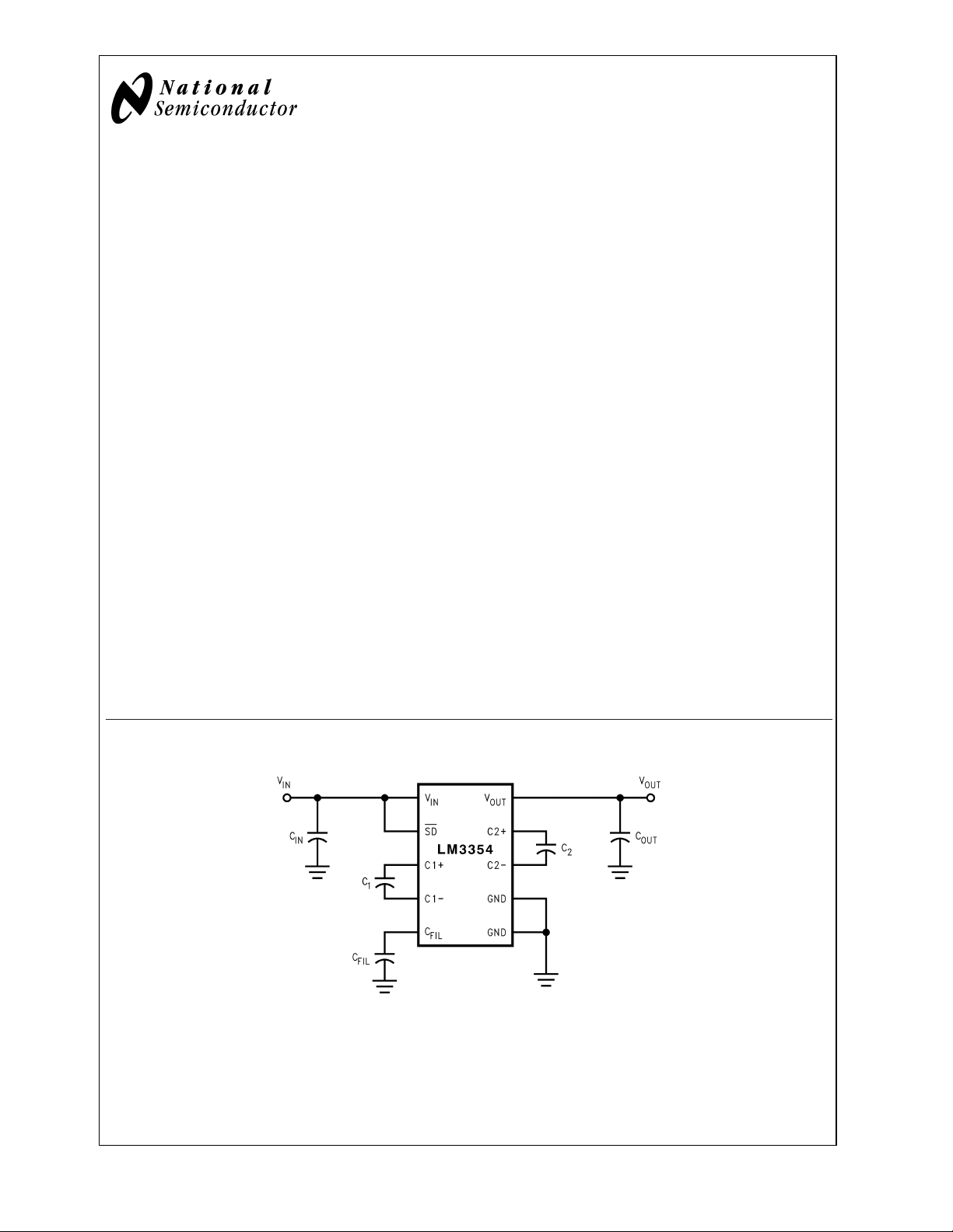
Typical Operating Circuit
20057301
© 2002 National Semiconductor Corporation DS200573 www.national.com
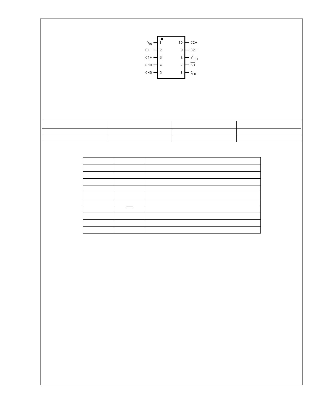
Connection Diagram
LM3354-3.7
Top View
MSOP-10 Pin Package
See NS Package Number MM
20057302
Ordering Information
Order Number Package Type NSC Package Drawing Supplied As
LM3354MMX-3.7 MSOP-10 MUB10A 3.5k Units, Tape and Reel
LM3354MM-3.7 MSOP-10 MUB10A 1k Units, Tape and Reel
Pin Description
Pin Number Name Function
1V
2 C1− Negative Terminal for C1
3 C1+ Positive Terminal for C1
4 GND Ground
5 GND Ground
6C
7SD
8V
9 C2− Negative Terminal for C2
10 C2+ Positive Terminal for C2
IN
FIL
OUT
Input Supply Voltage
Filter Capacitor, a 1µF capacitor is recommended.
Shutdown, active low
Regulated Output Voltage
www.national.com 2
LM3354-3.7
Absolute Maximum Ratings (Note 1)
If Military/Aerospace specified devices are required,
please contact the National Semiconductor Sales Office/
ESD Rating (Note 3)
Human Body Model
Machine Model
1.5 kV
Distributors for availability and specifications.
All Pins −0.5V to 5.6V
Power Dissipation (T
= 25˚C)
A
(Note 2) Internally Limited
(Note 2) 150˚C
T
JMAX
θ
(Note 2) 250˚C/W
JA
Storage Temperature −65˚C to +150˚C
Operating Ratings
Input Voltage (VIN) 2.5V to 5.5V
Output Voltage (V
Ambient Temperature (T
Junction Temperature (T
) 1.8V to 5.0V
OUT
) (Note 2) −40˚C to +85˚C
A
) (Note 2) −40˚C to +120˚C
J
Lead Temperature (Soldering, 5
sec.) 260˚C
Electrical Characteristics
Limits in standard typeface are for TA= 25˚C, and limits in boldface type apply over the full operating temperature range. Unless otherwise specified: C
= 0.33 µF; CIN= 10 µF; C
1=C2
Parameter Conditions Min
(Note 5)
LM3354-3.7
Output Voltage (V
OUT
)
Efficiency I
Output Voltage
Ripple
(Peak-to-Peak)
V
= (2.7, 5.5) V
IN
= (1, 70) mA
I
L
V
= (2.8, 4.0) V
IN
= (1, 90) mA
I
L
V
= (4.3, 5.5) V
IN
= (1, 90) mA
I
L
=15mA 75
LOAD
I
=70mA 70
LOAD
=50mA
I
LOAD
=10µF
C
OUT
3.589/3.552 3.7 3.811/3.848
3.589/3.552 3.7 3.811/3.848
3.589/3.552 3.7 3.811/3.848
ceramic
LM3354-ALL OUTPUT VOLTAGE VERSIONS
Operating Quiescent
Current
Shutdown Quiescent
Current
Switching
Measured at Pin
;
V
IN
= 0A (Note 6)
I
LOAD
SD Pin at 0V (Note
7)
0.6 1 1.4 MHz
Frequency
<
SD Input Threshold
2.5V
<
V
5.5V 0.2 V
IN
Low
SD Input Threshold
2.5V<V
<
5.5V 0.8 V
IN
IN
High
SD Input Current Measured at SD
Pin;
SD Pin = V
Note 1: “Absolute Maximum Ratings” indicate limits beyond which damage to the device may occur. Operating Ratings are conditions for which the device is
intended to be functional, but device parameter specifications may not be guaranteed. For guaranteed specifications and test conditions, see “Electrical
Characteristics”.
Note 2: As long as T
The 5V option requires that T
Note 3: The human body model is a 100 pF capacitor discharged through a 1.5 kΩ resistor into each pin. The machine model is a 200 pF capacitor discharged
directly into each pin.
Note 4: Typical numbers are at 25˚C and represent the most likely norm.
Note 5: All limits guaranteed at room temperature (standard typeface) and at temperature extremes (bold typeface). All room temperature limits are 100% tested
or guaranteed through statistical analysis. All limits at temperature extremes are guaranteed by correlation using standard Statistical Quality Control methods (SQC).
All limits are used to calculate Average Outgoing Quality Level (AOQL).
≤ +85˚C, all electrical characteristics hold true and the junction temperature should remain below +120˚C except for the 5V output option.
A
≤ +60˚C.
A
IN
= 5.5V
OUT
= 10 µF; C
(Note 4)
= 1 µF; VIN= 3.5V.
FIL
Typ
Max
(Note 5)
75 mV
375 475 µA
2.3 5 µA
IN
0.3 µA
Units
V
%
P-P
V
V
100V
www.national.com3

Electrical Characteristics (Continued)
Note 6: The V
Note 7: The output capacitor C
LM3354-3.7
pin is forced to 200 mV above the typical V
OUT
is fully discharged before measurement.
OUT
. This is to insure that the internal switches are off.
OUT
www.national.com 4
 Loading...