

NSC LM330T-5.0 Datasheet
LM330
3-Terminal Positive Regulator
LM330 3-Terminal Positive Regulator
May 1998
General Description
The LM330 5V 3-terminal positive voltage regulator features
an ability to source 150 mA of output current with an
input-output differential of 0.6V or less. Familiar regulator
features such as current limit and thermal overload protection are also provided.
The low dropout voltage makes the LM330 useful for certain
battery applications since thisfeatureallows a longer battery
discharge before the output falls out of regulation. For example, a battery supplying the regulator input voltage may
discharge to 5.6V and still properly regulate the system and
load voltage. Supporting this feature, the LM330 protects
both itself and regulated systems from negative voltage inputs resulting from reverse installations of batteries.
Other protection features include line transient protection up
to 26V, when the output actually shuts down to avoid damaging internal and external circuits. Also, the LM330 regulator
cannot be harmed by a temporary mirror-image insertion.
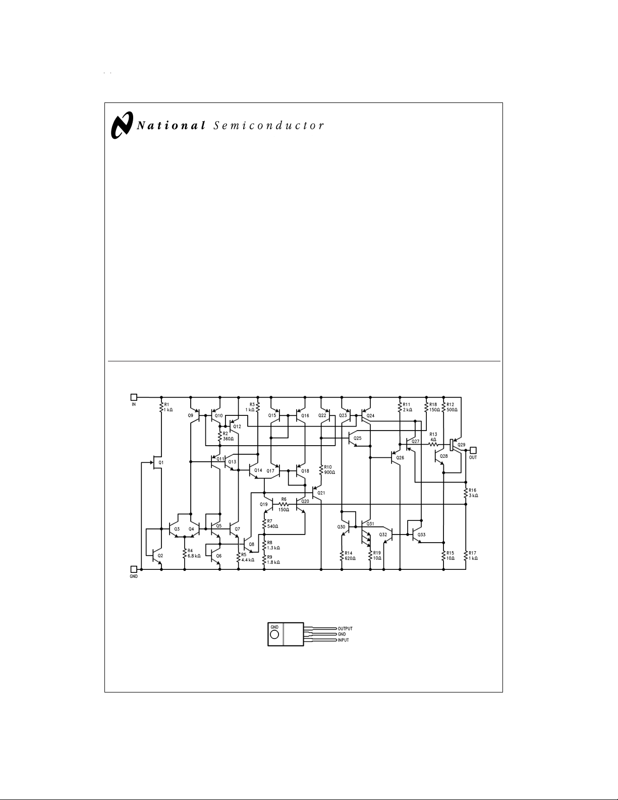
Schematic and Connection Diagrams
Features
n Input-output differential less than 0.6V
n Output current of 150 mA
n Reverse battery protection
n Line transient protection
n Internal short circuit current limit
n Internal thermal overload protection
n Mirror-image insertion protection
+
n P
Product Enhancement tested
DS009306-1
(TO-220)
Plastic Package
DS009306-2
Front View
Order Number LM330T-5.0
See NS Package Number T03B
© 1999 National Semiconductor Corporation DS009306 www.national.com
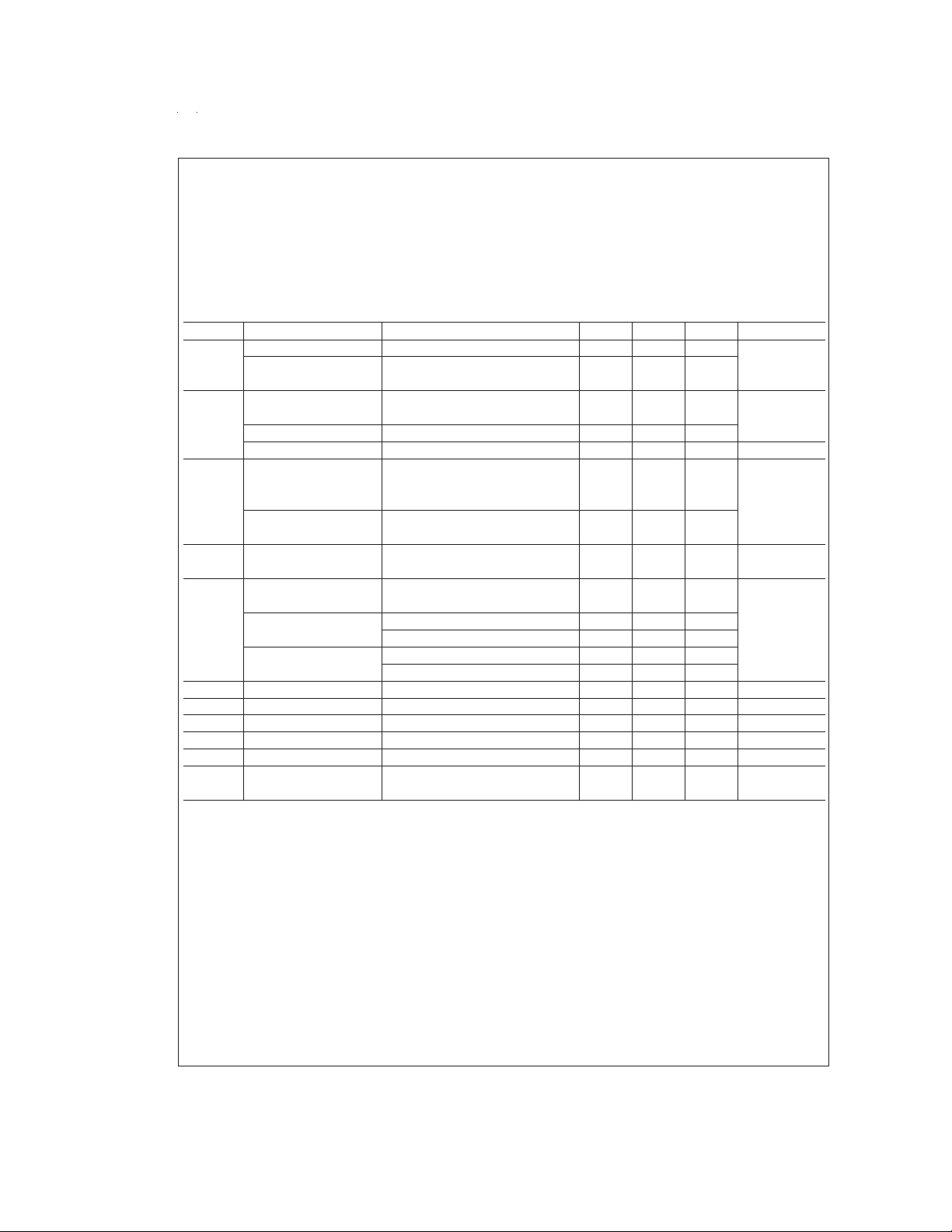
Absolute Maximum Ratings (Note 1)
If Military/Aerospace specified devices are required,
please contact the National Semiconductor Sales Office/
Distributors for availability and specifications.
Input Voltage
Operating Range 26V
Internal Power Dissipation Internally Limited
Operating Temperature Range 0˚C to +70˚C
Maximum Junction Temperature +125˚C
Storage Temperature Range −65˚C to +150˚C
Lead Temperature
(Soldering, 10 sec.) +300˚C
Line Transient Protection (1000 ms) 40V
Electrical Characteristics (Note 2)
Symbol Parameter Conditions Min Typ Max Units
V
o
Output Voltage T
Output Voltage 5
Over Temp 6
∆V
o
Line Regulation 9<V
Load Regulation 5
Long Term Stability 20 mV/1000 hrs
I
Q
Quiescent Current I
Line Transient V
Reverse Polarity V
∆I
Q
Quiescent Current 6<V
Change
V
IN
Overvoltage Shutdown 26 38
Voltage
Max Line Transient 60 V
Reverse Polarity −30
Input Voltage DC V
Output Noise Voltage 10 Hz–100 kHz 50 µV
Output Impedance I
Ripple Rejection 56 dB
Current Limit 150 400 700 mA
Dropout Voltage I
Thermal Resistance Junction to Case 4 ˚C/W
Note 1: “Absolute Maximum Ratings” indicate limits beyond which damage to the device may occur. Operating Ratings indicate conditions for which the device is
functional, but do not guarantee specific performance limits.
Note 2: Unless otherwise specified: V
measured using pulse techniques (t
rately.
=
IN
≤ 10 ms, duty cycle ≤ 5%). Output voltage changes due to changes in internal temperature must be taken into account sepa-
W
=
25˚C 4.8 5 5.2
j
<
<
I
150 mA 4.75 5.25 V
o
<
<
V
26V; 0˚C ≤ Tj≤ 100˚C
IN
<
IN
<
<
6
V
IN
<
<
I
o
=
10 mA 3.5 7
o
=
I
50 mA 5 11
o
=
I
150 mA 18 40 mA
o
=
40V, R
IN
=
−6V, R
IN
<
IN
1s, V
≤ 5.5V 50
o
>
o
=
100 mADC + 10 mArms 200 mΩ
o
=
150 mA 0.32 0.6 V
o
=
16V, I
26V, I
5mA 7 25
o
=
5mA 30 60 mV
o
150 mA 14 50
=
100Ω,1s 14
L
=
100Ω −80
L
26V 10
− 0.3V, R
=
100Ω −12
L
Junction to Ambient 50
14V, I
=
o
150 mA, T
=
25˚C, C1=0.1 µF, C2=10 µF. All characteristics except noise voltage and ripple rejection are
j
%
www.national.com 2
 Loading...