

NSC LM3302N Datasheet
LM139/LM239/LM339/LM2901/LM3302
Low Power Low Offset Voltage Quad Comparators
General Description
The LM139 series consists of four independent precision
voltage comparators with an offset voltage specification as
low as 2 mV max for all four comparators. These were designed specifically to operate from a single power supply
over a wide range of voltages. Operation from split power
supplies is also possible and the low power supply current
drain is independent of the magnitude of the power supply
voltage. These comparatorsalso have a unique characteristic in that the input common-mode voltage range includes
ground, even though operated from a single power supply
voltage.
Application areas include limit comparators, simple analog to
digital converters; pulse, squarewave and time delay generators; wide range VCO; MOS clock timers; multivibrators
and high voltage digital logic gates. The LM139 series was
designed to directly interface with TTL and CMOS. When operated from both plus and minus power supplies, they will directly interface with MOS logic— where the low power drain
of the LM339 is a distinct advantage over standard comparators.
Advantages
n High precision comparators
n Reduced V
n Eliminates need for dual supplies
n Allows sensing near GND
n Compatible with all forms of logic
n Power drain suitable for battery operation
Features
n Wide supply voltage range
— LM139/139A Series 2 to 36 V
— LM2901: 2 to 36 V
— LM3302: 2 to 28 V
n Very low supply current drain (0.8 mA) — independent
of supply voltage
n Low input biasing current: 25 nA
n Low input offset current:
n Offset voltage:
n Input common-mode voltage range includes GND
n Differential input voltage range equal to the power
supply voltage
n Low output saturation voltage: 250 mV at 4 mA
n Output voltage compatible with TTL, DTL, ECL, MOS
and CMOS logic systems
drift over temperature
OS
or±1to±18 V
DC
DC
DC
or±1to±18 V
or±1to±14 V
November 1999
±
5nA
±
3mV
LM139/LM239/LM339/LM2901/LM3302 Low Power Low Offset Voltage Quad Comparators
DC
DC
DC
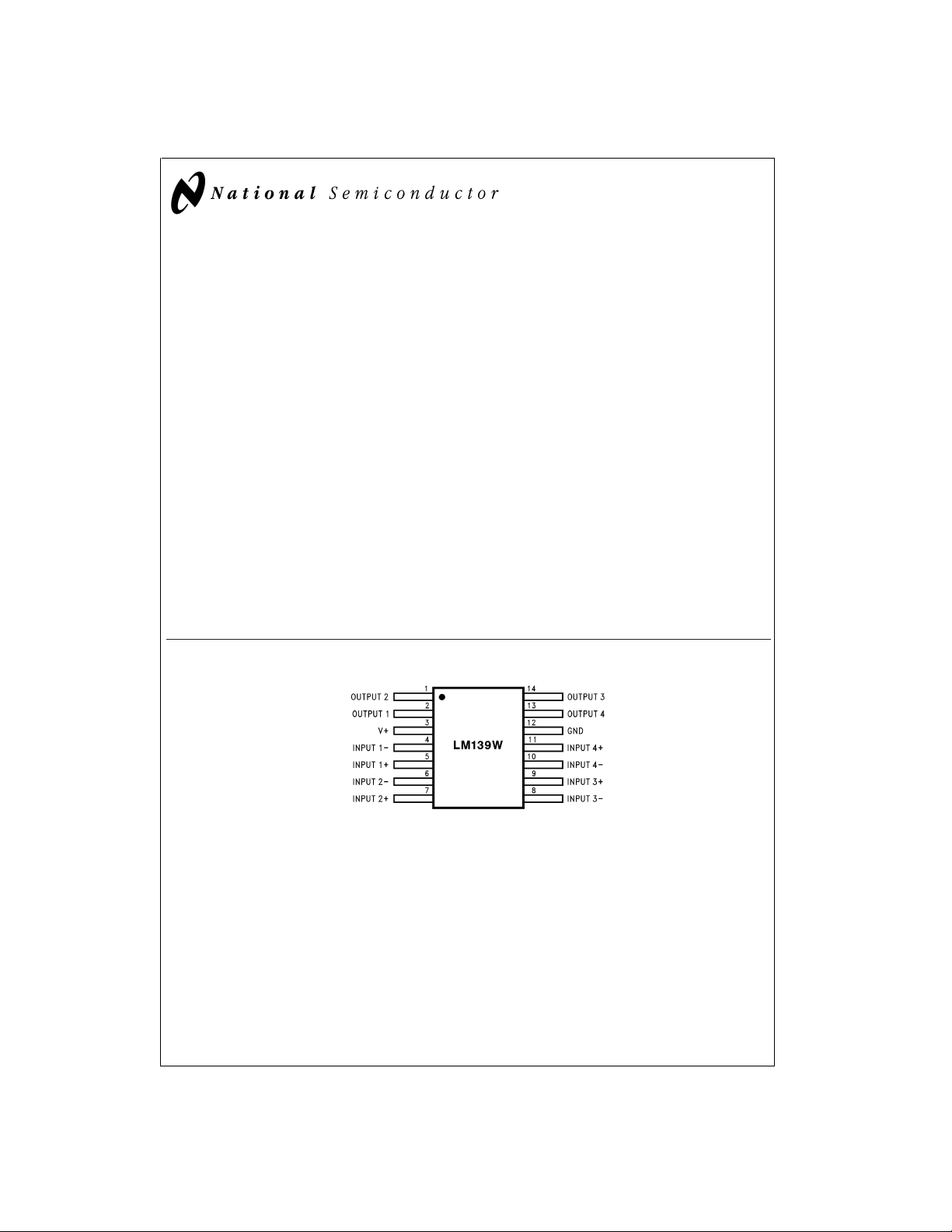
Connection Diagrams
DS005706-27
Order Number LM139AW/883 or LM139W/883 (Note 1)
LM139AWRQML and LM139AWRQMLV(Note 3)
See NS Package Number W14B
LM139AWGRQML and LM139AWGRQMLV(Note 3)
See NS Package Number WG14A
© 1999 National Semiconductor Corporation DS005706 www.national.com
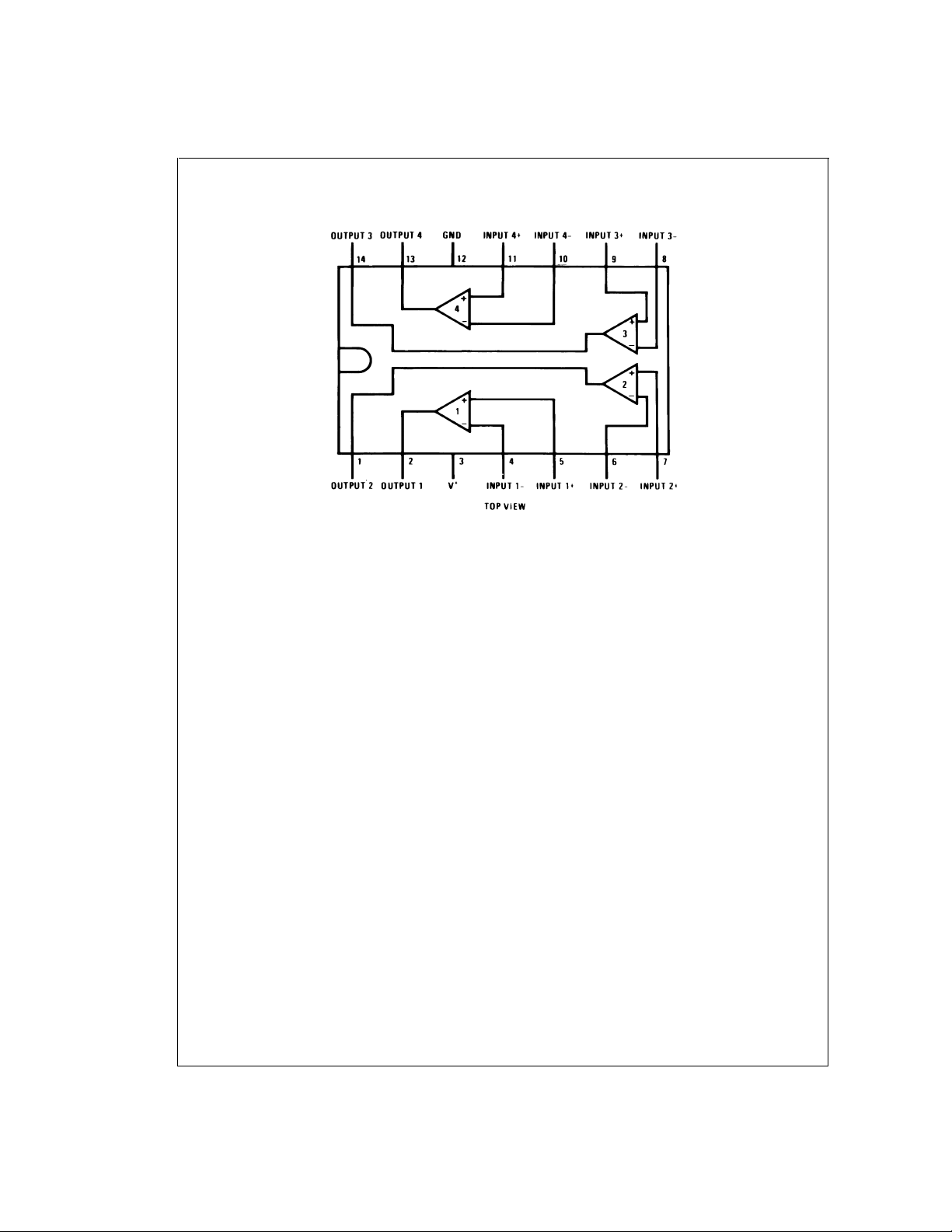
Connection Diagrams (Continued)
LM139/LM239/LM339/LM2901/LM3302
Order Number LM139J, LM139J/883 (Note 1), LM139AJ,
LM139AJ/883 (Note 2), LM239J, LM239AJ, LM339J,
LM139AJRQML and LM139AJRQMLV(Note 3)
Order Number LM339AM, LM339M or LM2901M
Order Number LM339N, LM339AN, LM2901N or LM3302N
Note 1: Available per JM38510/11201
Note 2: Available per SMD
Note 3: See STD Mil Dwg 5962R96738 for Radiation TolerantDevice
#
5962-8873901
Dual-In-Line Package
DS005706-2
See NS Package Number J14A
See NS Package Number M14A
See NS Package Number N14A
www.national.com 2
Absolute Maximum Ratings (Note 13)
If Military/Aerospace specified devices are required, please contact the National Semiconductor Sales Office/
Distributors for availability and specifications.
LM139/LM239/LM339
LM139A/LM239A/LM339A LM3302
Supply Voltage, V
+
Differential Input Voltage (Note 11) 36 V
Input Voltage −0.3 VDCto +36 V
Input Current (V
<
−0.3 VDC),
IN
(Note 6) 50 mA 50 mA
Power Dissipation (Note 4)
Molded DIP 1050 mW 1050 mW
Cavity DIP 1190 mW
Small Outline Package 760 mW
Output Short-Circuit to GND,
(Note 5) Continuous Continuous
Storage Temperature Range −65˚C to +150˚C −65˚C to +150˚C
Lead Temperature
(Soldering, 10 seconds) 260˚C 260˚C
Operating Temperature Range −40˚C to +85˚C
LM339/LM339A 0˚C to +70˚C
LM239/LM239A −25˚C to +85˚C
LM2901 −40˚C to +85˚C
LM139/LM139A −55˚C to +125˚C
Soldering Information
Dual-In-Line Package
Soldering (10 seconds) 260˚C 260˚C
Small Outline Package
Vapor Phase (60 seconds) 215˚C 215˚C
Infrared (15 seconds) 220˚C 220˚C
See AN-450 “Surface Mounting Methods and Their Effect on Product Reliability” for other methods of soldering surface mount
devices.
ESD rating (1.5 kΩ in series with 100 pF) 600V 600V
LM2901
36 VDCor±18 V
DC
DC
DC
28 VDCor±14 V
28 V
DC
−0.3 VDCto +28 V
DC
DC
LM139/LM239/LM339/LM2901/LM3302
Electrical Characteristics
+
=
(V
5V
=
25˚C, unless otherwise stated)
DC,TA
Parameter Conditions LM139A LM239A, LM339A LM139 Units
Min Typ Max Min Typ Max Min Typ Max
Input Offset Voltage (Note 12) 1.0 2.0 1.0 2.0 2.0 5.0 mV
Input Bias Current I
Input Offset Current I
Input Common-Mode V
Voltage Range V
Supply Current R
Voltage Gain R
Large Signal V
Response Time 1.4 V
Response Time V
or I
IN(+)
Linear Range, (Note 8), V
IN(+)−IIN(−),VCM
+
=
+
=
=
L
=
R
L
(LM3302, V
≥15 kΩ,V
L
=
V
o
=
IN
=
R
L
RL
with Output in 25 100 25 250 25 100 nA
IN(−)
=
0V 3.0 25 5.0 50 3.0 25 nA
(LM3302, 0 V+−1.5 0 V+−1.5 0 V+−1.5 V
30 V
DC
) (Note 9)
28 V
DC
∞
on all Comparators, 0.8 2.0 0.8 2.0 0.8 2.0 mA
+
=
∞
,V
36V, 1.0 2.5 1.0 2.5 mA
+
=
28 V
DC
+
=
15 V
to 11 V
1V
DC
DC
TTL Logic Swing, V
=
5V
DC,VRL
DC
=
0V
CM
)
DC
REF
50 200 50 200 50 200 V/mV
=
300 300 300 ns
,
5.1 kΩ
=
5V
=
5.1 kΩ, 1.3 1.3 1.3 µs
DC,RL
(Note 10)
www.national.com3
DC
DC
DC
DC
DC
DC
Electrical Characteristics (Continued)
+
=
(V
5V
Parameter Conditions LM139A LM239A, LM339A LM139 Units
Output Sink Current V
Saturation Voltage V
Output Leakage V
Current V
Electrical Characteristics
LM139/LM239/LM339/LM2901/LM3302
+
=
(V
5V
Parameter Conditions LM239, LM339 LM2901 LM3302 Units
Input Offset Voltage (Note 12) 2.0 5.0 2.0 7.0 3 20 mV
Input Bias Current I
Input Offset Current I
Input Common-Mode V
Voltage Range V
Supply Current R
Voltage Gain R
Large Signal V
Response Time 1.4 V
Response Time V
Output Sink Current V
Saturation Voltage V
Output Leakage V
Current V
=
25˚C, unless otherwise stated)
DC,TA
VO≤1.5 V
I
SINK
=
25˚C, unless otherwise stated)
DC,TA
IN(+)
Linear Range, (Note 8), V
IN(+)−IIN(−),VCM
R
(LM3302, V
V
R
(Note 10)
VO≤1.5 V
I
SINK
Min Typ Max Min Typ Max Min Typ Max
IN(−)
IN(−)
=
=
1V
DC
1V
DC,VIN(+)
DC,VIN(+)
=
0, 6.0 16 6.0 16 6.0 16 mA
=
0, 250 400 250 400 250 400 mV
≤4mA
IN(+)
O
=
=
5V
1V
DC
DC,VIN(−)
=
0, 0.1 0.1 0.1 nA
Min Typ Max Min Typ Max Min Typ Max
or I
with Output in 25 250 25 250 25 500 nA
IN(−)
=
+
=
30 V
+
=
28 V
=
∞
on all Comparators, 0.8 2.0 0.8 2.0 0.8 2.0 mA
L
=
∞
,V
L
≥15 kΩ,V
L
=
1V
o
=
TTL Logic Swing, V
IN
DC,VRL
=
5.1 kΩ,
L
=
5V
RL
=
1V
IN(−)
=
1V
IN(−)
0V 5.0 50 5 50 3 100 nA
(LM3302, 0 V+−1.5 0 V+−1.5 0 V+−1.5 V
DC
) (Note 9)
DC
+
=
36V, 1.0 2.5 1.0 2.5 1.0 2.5 mA
+
=
28 V
DC
+
=
15 V
to 11 V
DC
DC,RL
DC
=
5V
DC
=
5.1 kΩ, 1.3 1.3 1.3 µs
DC,VIN(+)
DC
DC,VIN(+)
=
0V
CM
)
DC
REF
50 200 25 100 2 30 V/mV
=
300 300 300 ns
,
=
0, 6.0 16 6.0 16 6.0 16 mA
=
0, 250 400 250 400 250 500 mV
≤4mA
IN(+)
O
=
=
5V
1V
DC
DC,VIN(−)
=
0, 0.1 0.1 0.1 nA
DC
DC
DC
DC
DC
DC
DC
DC
DC
DC
DC
DC
Electrical Characteristics
+
=
(V
, (Note 7))
5.0 V
DC
Parameter Conditions
LM139A LM239A,
LM339A
LM139
Min Typ Max Min Typ Max Min Typ Max
Input Offset Voltage (Note 12) 4.0 4.0 9.0 mV
Input Offset Current I
Input Bias Current I
IN(+)−IIN(−),VCM
or I
IN(+)
Linear Range, V
+
Input Common-Mode V
Voltage Range V
Saturation Voltage V
www.national.com 4
=
30 V
+
=
28 V
=
IN(−)
I
≤4mA
SINK
=
0V 100 150 100 nA
with Output in 300 400 300 nA
IN(−)
DC
DC
1V
=
0V (Note 8)
CM
(LM3302, 0 V+−2.0 0 V+−2.0 0 V+−2.0 V
) (Note 9)
=
DC,VIN(+)
0, 700 700 700 mV
Units
DC
DC
DC
DC
DC
Electrical Characteristics (Continued)
+
=
(V
Output Leakage Current V
Differential Input Voltage Keep all V
Electrical Characteristics
+
=
(V
Input Offset Voltage (Note 12) 9.0 9 15 40 mV
Input Offset Current I
Input Bias Current I
Input Common-Mode V
Voltage Range (Note 9)
Saturation Voltage V
Output Leakage Current V
Differential Input Voltage Keep all V
Note 4: For operating at high temperatures, the LM339/LM339A,LM2901,LM3302mustbederatedbased on a 125˚C maximum junction temperature and a thermal
resistance of 95˚C/W which applies for the device soldered in a printed circuit board, operating in a still air ambient. The LM239 and LM139 must be derated based
on a 150˚C maximum junction temperature. The low bias dissipation and the “ON-OFF” characteristic of the outputs keeps the chip dissipation very small(P
mW), provided the output transistors are allowed to saturate.
Note 5: Short circuits from the output to V
current is approximately 20 mA independent of the magnitude of V
Note 6: This input current will only exist when the voltage at any of the input leads is driven negative. It is due to the collector-base junction of the input PNP transistors becoming forward biased and thereby acting as input diode clamps. In addition to this diode action, there is also lateral NPN parasitic transistor action on the
IC chip. This transistor action can cause the output voltages of the comparators to go to the V
that an input is driven negative. This is not destructive and normal output states will re-establish when the input voltage, which was negative, again returns to a value
greater than −0.3 V
Note 7: These specifications are limited to −55˚C≤T
−25˚C≤T
Note 8: The direction of the input current is out of the IC due to the PNP input stage. This current is essentially constant, independent of the state of the outputso
no loading change exists on the reference or input lines.
Note 9: The input common-mode voltage or either input signal voltage should not be allowed to go negative by more than 0.3V.The upper end of the common-mode
voltage range is V
Note 10: The response time specified is a 100 mV input step with 5 mV overdrive. For larger overdrive signals 300 ns can be obtained, see typical performance char-
acteristics section.
Note 11: Positive excursions of input voltage may exceed the power supply level. As long as the other voltage remains within the common-mode range, the com-
parator will provide a proper output state. The low input voltage state must not be less than −0.3 V
if used) (at 25˚C).
Note 12: At output switch point, V
For LM3302, V
Note 13: Refer to RETS139AX for LM139A military specifications and to RETS139X for LM139 military specifications.
, (Note 7))
5.0 V
DC
Parameter Conditions
LM139A LM239A,
LM339A
LM139
Units
Min Typ Max Min Typ Max Min Typ Max
=
0, 1.0 1.0 1.0 µA
IN(−)
, (LM3302,
)
’s≥0VDC(or V−,363636V
IN
V
V
IN(+)
O
O
=
=
1VDC,V
=
30 V
28 V
DC
DC
if used), (Note 11)
, (Note 7))
5.0 V
DC
Parameter Conditions LM239, LM339 LM2901 LM3302 Units
Min Typ Max Min Typ Max Min Typ Max
=
IN(+)−IIN(−),VCM
or I
IN(+)
Linear Range, V
8)
+
=
30 V
)
V
DC
=
1V
IN(−)
I
≤4mA
SINK
1VDC,V
=
IN(+)
=
V
30 V
O
)
V
DC
0V 150 50 200 300 nA
with Output in 400 200 500 1000 nA
IN(−)
DC
DC
=
0V (Note
CM
+
(LM3302, V
DC,VIN(+)
, (LM3302, V
’s≥0VDC(or V−,363628V
IN
=
28
=
0, 700 400 700 700 mV
=
0, 1.0 1.0 1.0 µA
IN(−)
=
28
O
+
V
−2.0 0 V+−2.0 0 V+−2.0 V
if used), (Note 11)
≤100
D
+
can cause excessive heating and eventual destruction. When considering short circuits to ground, the maximum output
(at 25˚)C.
DC
≤+85˚C, the LM339/LM339A temperature specifications are limited to 0˚C≤TA≤+70˚C, and the LM2901, LM3302 temperature range is −40˚C≤TA≤+85˚C.
A
+
−1.5V at 25˚C, but either or both inputs can go to +30 VDCwithout damage (25V for LM3302), independent of the magnitude of V+.
≅
1.4 VDC,R
+
from 5 VDCto 28 VDC.
O
=
0ΩwithV
S
A
+
.
+
voltage level (or to ground for a large overdrive) for the time duration
≤+125˚C, for the LM139/LM139A. With the LM239/LM239A, all temperature specifications are limited to
(or 0.3 VDCbelow the magnitude of the negative power supply,
DC
+
from 5 VDCto 30 VDC; and over the full input common-mode range (0 VDCto V+−1.5 VDC), at 25˚C.
LM139/LM239/LM339/LM2901/LM3302
DC
DC
DC
DC
DC
DC
DC
DC
DC
www.national.com5
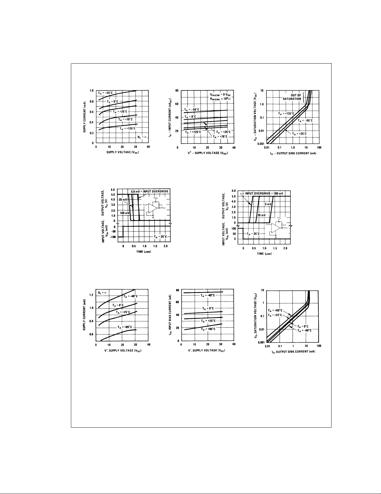
Typical Performance Characteristics LM139/LM239/LM339, LM139A/LM239A/LM339A, LM3302
Supply Current
LM139/LM239/LM339/LM2901/LM3302
DS005706-34
Response Time for Various
Input Overdrives— Negative
Transition
DS005706-37
Input Current
Output Saturation Voltage
DS005706-35
Response Time for Various
Input Overdrives— Positive
Transition
DS005706-36
DS005706-38
Typical Performance Characteristics LM2901
Supply Current
DS005706-39
www.national.com 6
Input Current
DS005706-40
Output Saturation Voltage
DS005706-41
 Loading...