

LM2940/LM2940C
1A Low Dropout Regulator
General Description
The LM2940/LM2940C positive voltage regulator features
the ability to source 1A of output current with a dropout
voltage of typically 0.5V and a maximum of 1V over the
entire temperature range. Furthermore, a quiescent current
reduction circuit has been included which reduces the
ground current when the differential between the input voltage and the output voltage exceeds approximately 3V. The
quiescent current with 1A of output current and an inputoutput differential of 5V is therefore only 30 mA. Higher
quiescent currents only exist when the regulator is in the
dropout mode (V
IN−VOUT
≤ 3V).
Designed also for vehicular applications, the LM2940/
LM2940C and all regulated circuitry are protected from reverse battery installations or 2-battery jumps. During line
transients, such as load dump when the input voltage can
momentarily exceed the specified maximum operating voltage, the regulator will automatically shut down to protect
both the internal circuits and the load. The LM2940/
LM2940C cannot be harmed by temporary mirror-image insertion. Familiar regulator features such as short circuit and
thermal overload protection are also provided.
Features
n Dropout voltage typically 0.5V@IO=1A
n Output current in excess of 1A
n Output voltage trimmed before assembly
n Reverse battery protection
n Internal short circuit current limit
n Mirror image insertion protection
n P
+
Product Enhancement tested
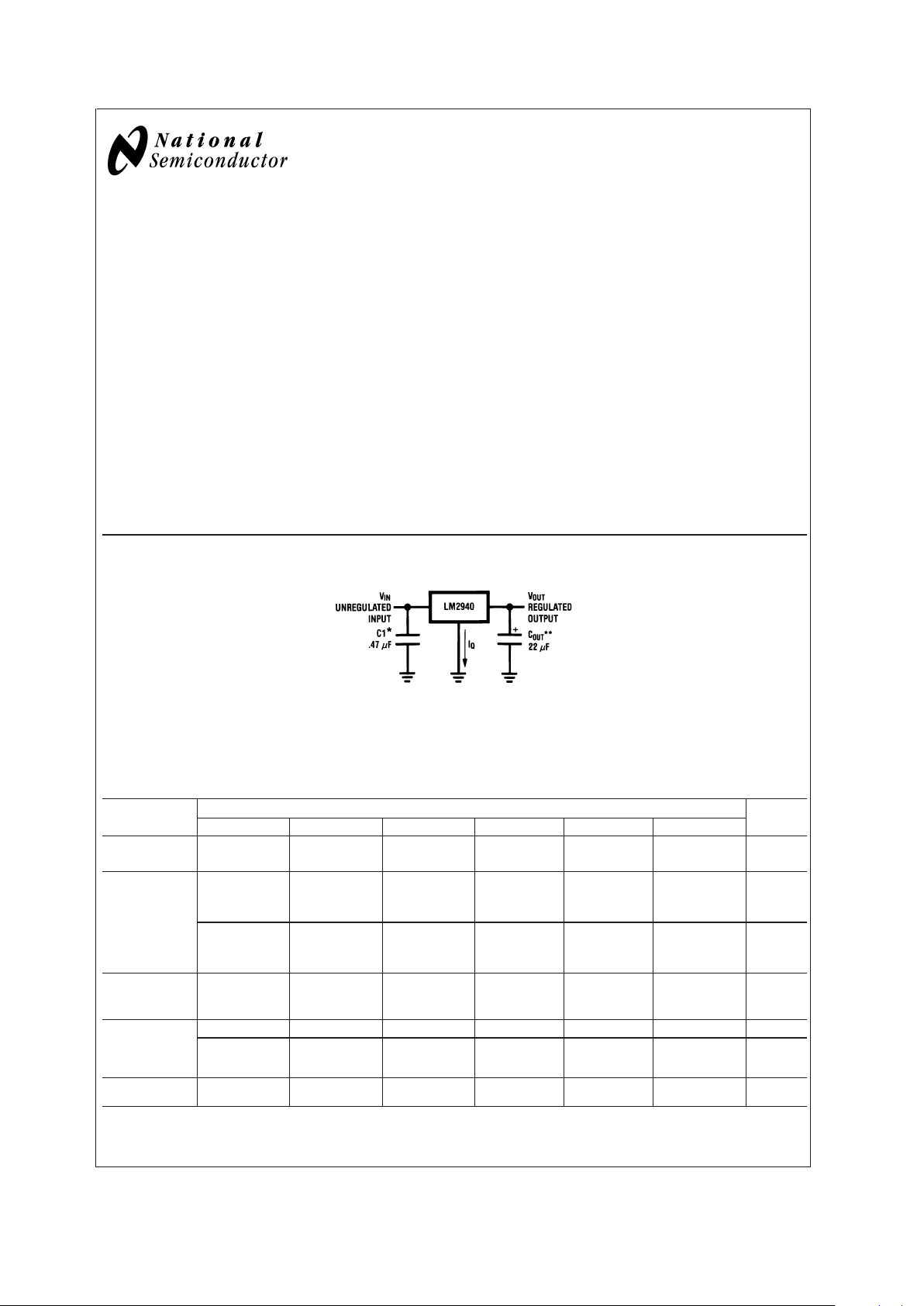
Typical Application
00882203
*
Required if regulator is located far from power supply filter.
**
C
OUT
must be at least 22 µF to maintain stability. May be increased without bound to maintain regulation during transients. Locate as close as possible
to the regulator. This capacitor must be rated over the same operating temperature range as the regulator and the ESR is critical; see curve.
Ordering Information
Temperature
Range
Output Voltage
Package
5.0 8.0 9.0 10 12 15
0˚C ≤ T
J
≤ 125˚C LM2940CT-5.0 LM2940CT-9.0 LM2940CT-12 LM2940CT-15 TO-220
LM2940CS-5.0 LM2940CS-9.0 LM2940CS-12 LM2940CS-15 TO-263
−40˚C ≤ T
J
≤
125˚C
LM2940LD-5.0 LM2940LD-8.0 LM2940LD-9.0 LM2940LD-10 LM2940LD-12 LM2940LD-15 LLP 1k
Units
Tape and
Reel
LM2940LDX-5.0 LM2940LDX-8.0 LM2940LDX-9.0 LM2940LDX-10 LM2940LDX-12 LM2940LDX-15 LLP 4.5k
Units
Tape and
Reel
−40˚C ≤ T
J
≤
125˚C
LM2940T-5.0 LM2940T-8.0 LM2940T-9.0 LM2940T-10 LM2940T-12 TO-220
LM2940S-5.0 LM2940S-8.0 LM2940S-9.0 LM2940S-10 LM2940S-12 TO-263
−40˚C ≤ T
J
≤
85˚C
LM2940IMP-5.0 LM2940IMP-8.0 LM2940IMP-9.0 LM2940IMP-10 LM2940IMP-12 LM2940IMP-15 SOT-223
LM2940IMPX-5.0 LM2940IMPX-8.0 LM2940IMPX-9.0 LM2940IMPX-10 LM2940IMPX-12 LM2940IMPX-15 SOT-223
in Tape
and Reel
SOT-223
Package Marking
L53B L54B L0EB L55B L56B L70B
The physical size of the SOT-223 is too small to contain the full device part number. The package markings indicated are what will appear on the actual device.
January 2003
LM2940/LM2940C 1A Low Dropout Regulator
© 2003 National Semiconductor Corporation DS008822 www.national.com
Ordering Information (Continued)
Temperature
Range
Output Voltage Package
5.0 8.0 12 15
−55˚C ≤ T
J
≤ 125˚C LM2940J-5.0/883
5962-8958701EA
LM2940J-8.0/883
5962-9088301QEA
LM2940J-12/883
5962-9088401QEA
LM2940J-15/883
5962-9088501QEA
J16A
LM2940WG5.0/883
5962-8958701XA
WG16A
For information on military temperature range products, please go to the Mil/Aero Web Site at http://www.national.com/appinfo/milaero/index.html.
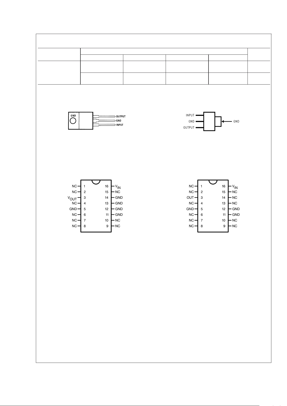
Connection Diagrams
(TO-220) Plastic Package 3-Lead SOT-223
00882202
Front View
Order Number LM2940CT-5.0, LM2940CT-9.0,
LM2940CT-12, LM2940CT-15, LM2940T-5.0,
LM2940T-8.0, LM2940T-9.0,
LM2940T-10 or LM2940T-12
See NS Package Number TO3B
00882242
Front View
Order Part Number LM2940IMP-5.0,
LM2940IMP-8.0, LM2940IMP-9.0,
LM2940IMP-10, LM2940IMP-12 or LM2940IMP-15
See NS Package Number MP04A
16-Lead Dual-in-Line Package (J)
00882243
Top View
Order Number LM2940J-5.0/883 (5962-8958701EA),
LM2940J-8.0/883 (5962-9088301QEA),
LM2940J-12/883 (5962-9088401QEA),
LM2940J-15/883 (5962-9088501QEA)
See NS Package Number J16A
16-Lead Ceramic Surface-Mount Package (WG)
00882244
Top View
Order Number LM2940WG5.0/883 (5962-8958701XA)
See NS Package Number WG16A
LM2940/LM2940C
www.national.com 2
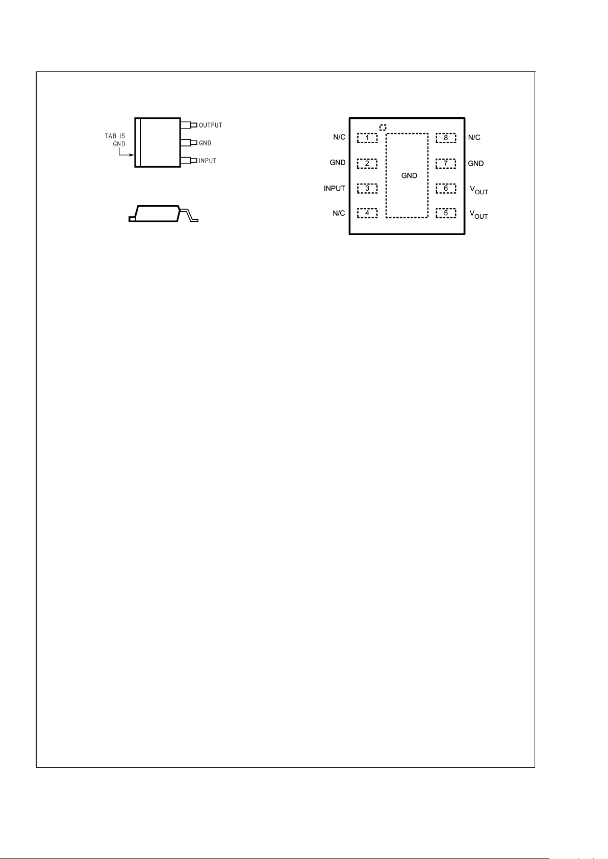
Connection Diagrams (Continued)
(TO-263) Surface-Mount Package
00882211
Top View
8-Lead LLP
00882246
Top View
Order Number LM2940LD-5.0, LM2940LD-8.0,
LM2940LD-9.0, LM2940LD-10,
LM2940LD-12, LM2940LD-15
See NS Package Number LDC08A
Pin 2 and pin 7 are fused to center DAP
Pin 5 ans 6 need to be tied together on PCB board
00882212
Side View
Order Number LM2940CS-5.0, LM2940CS-9.0,
LM2940CS-12, LM2940CS-15,
LM2940S-5.0, LM2940S-8.0,
LM2940S-9.0, LM2940S-10 or LM2940S-12
See NS Package Number TS3B
LM2940/LM2940C
www.national.com3
Absolute Maximum Ratings (Note 1)
If Military/Aerospace specified devices are required,
please contact the National Semiconductor Sales Office/
Distributors for availability and specifications.
LM2940S, T, MP ≤ 100 ms 60V
LM2940CS, T ≤ 1 ms 45V
Internal Power Dissipation
(Note 2) Internally Limited
Maximum Junction Temperature 150˚C
Storage Temperature Range −65˚C ≤ T
J
≤ +150˚C
Lead Temperature, Time for Wave Soldering
TO-220 (T) Package 260˚C, 10s
TO-263 (S) Package 260˚C, 4s
SOT-223 (MP) Package 260˚C, 4s
ESD Susceptibility (Note 3) 2 kV
Operating Conditions (Note 1)
Input Voltage 26V
Temperature Range
LM2940T, LM2940S −40˚C ≤ T
J
≤ 125˚C
LM2940CT, LM2940CS 0˚C ≤ T
J
≤ 125˚C
LM2940IMP −40˚C ≤ T
J
≤ 85˚C
LM2940J, LM2940WG −55˚C ≤ T
J
≤ 125˚C
LM2940LD −40˚C ≤ T
J
≤ 125˚C
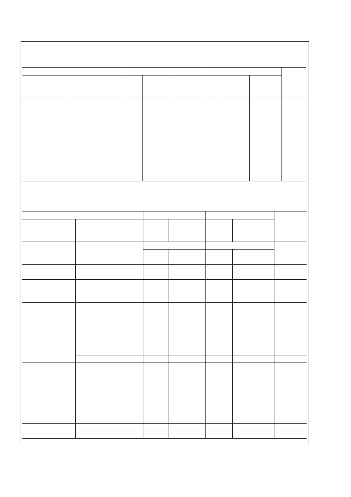
Electrical Characteristics
VIN=VO+ 5V, IO= 1A, CO= 22 µF, unless otherwise specified. Boldface limits apply over the entire operating temperature range of the indicated device. All other specifications apply for T
A=TJ
= 25˚C.
Output Voltage (V
O
)5V 8V
Units
LM2940 LM2940/883 LM2940 LM2940/883
Parameter Conditions Typ Limit Limit Typ Limit Limit
(Note 4) (Note 5) (Note 4) (Note 5)
6.25V ≤ V
IN
≤ 26V 9.4V ≤ VIN≤ 26V
Output Voltage 5 mA ≤ I
O
≤ 1A 5.00 4.85/4.75 4.85/4.75 8.00 7.76/7.60 7.76/7.60 V
MIN
5.15/5.25 5.15/5.25 8.24/8.40 8.24/8.40 V
MAX
Line Regulation VO+2V≤ VIN≤ 26V, 20 50 40/50 20 80 50/80 mV
MAX
IO=5mA
Load Regulation 50 mA ≤ I
O
≤ 1A
LM2940, LM2940/883 35 50/80 50/100 55 80/130 80/130 mV
MAX
LM2940C 35 50 55 80
Output 100 mADC and
Impedance 20 mArms, 35 1000/1000 55 1000/1000 mΩ
f
O
= 120 Hz
Quiescent V
O
+2V ≤ VIN≤ 26V,
Current I
O
=5mA
LM2940, LM2940/883 10 15/20 15/20 10 15/20 15/20 mA
MAX
LM2940C 10 15
V
IN=VO
+ 5V, 30 45/60 50/60 30 45/60 50/60 mA
MAX
IO=1A
Output Noise 10 Hz − 100 kHz, 150 700/700 240 1000/1000 µV
rms
Voltage IO=5mA
Ripple Rejection f
O
= 120 Hz, 1 V
rms
,
I
O
= 100 mA
LM2940 72 60/54 66 54/48 dB
MIN
LM2940C 72 60 66 54
f
O
= 1 kHz, 1 V
rms
, 60/50 54/48 dB
MIN
IO=5mA
Long Term 20 32 mV/
Stability 1000 Hr
Dropout Voltage I
O
= 1A 0.5 0.8/1.0 0.7/1.0 0.5 0.8/1.0 0.7/1.0 V
MAX
IO= 100 mA 110 150/200 150/200 110 150/200 150/200 mV
MAX
Short Circuit
Current
(Note 6)
1.9 1.6 1.5/1.3 1.9 1.6 1.6/1.3 A
MIN
LM2940/LM2940C
www.national.com 4
Electrical Characteristics (Continued)
VIN=VO+ 5V, IO= 1A, CO= 22 µF, unless otherwise specified. Boldface limits apply over the entire operating temperature range of the indicated device. All other specifications apply for T
A=TJ
= 25˚C.
Output Voltage (V
O
)5V 8V
Units
LM2940 LM2940/883 LM2940 LM2940/883
Parameter Conditions Typ Limit Limit Typ Limit Limit
(Note 4) (Note 5) (Note 4) (Note 5)
Maximum Line R
O
= 100Ω
V
MIN
Transient LM2940, T ≤ 100 ms 75 60/60 75 60/60
LM2940/883, T ≤ 20 ms 40/40 40/40
LM2940C, T ≤ 1ms 5545 5545
Reverse Polarity R
O
= 100Ω
DC Input Voltage LM2940, LM2940/883 −30 −15/−15 −15/−15 −30 −15/−15 −15/−15 V
MIN
LM2940C −30 −15 −30 −15
Reverse Polarity R
O
= 100Ω
Transient Input LM2940, T ≤ 100 ms −75 −50/−50 −75 −50/−50 V
MIN
Voltage LM2940/883, T ≤ 20 ms −45/−45 −45/−45
LM2940C, T ≤ 1 ms −55 −45/−45
Electrical Characteristics
VIN=VO+ 5V, IO= 1A, CO= 22 µF, unless otherwise specified. Boldface limits apply over the entire operating temperature range of the indicated device. All other specifications apply for T
A=TJ
= 25˚C.
Output Voltage (V
O
) 9V 10V
Units
Parameter Conditions Typ
LM2940
Typ
LM2940
Limit Limit
(Note 4) (Note 4)
10.5V ≤ V
IN
≤ 26V 11.5V ≤ VIN≤ 26V
Output Voltage 5 mA ≤ I
O
≤1A 9.00 8.73/8.55 10.00 9.70/9.50 V
MIN
9.27/9.45 10.30/10.50 V
MAX
Line Regulation VO+2V≤ VIN≤ 26V, 20 90 20 100 mV
MAX
IO=5mA
Load Regulation 50 mA ≤ I
O
≤ 1A
LM2940 60 90/150 65 100/165 mV
MAX
LM2940C 60 90
Output Impedance 100 mADC and
20 mArms, 60 65 mΩ
f
O
= 120 Hz
Quiescent V
O
+2V ≤ V
IN
<
26V,
Current I
O
=5mA
LM2940 10 15/20 10 15/20 mA
MAX
LM2940C 10 15
V
IN=VO
+ 5V, IO= 1A 30 45/60 30 45/60 mA
MAX
Output Noise 10 Hz − 100 kHz, 270 300 µV
rms
Voltage IO=5mA
Ripple Rejection f
O
= 120 Hz, 1 V
rms
,
I
O
= 100 mA
LM2940 64 52/46 63 51/45 dB
MIN
LM2940C 64 52
Long Term
Stability
34 36 mV/
1000 Hr
Dropout Voltage I
O
= 1A 0.5 0.8/1.0 0.5 0.8/1.0 V
MAX
IO= 100 mA 110 150/200 110 150/200 mV
MAX
LM2940/LM2940C
www.national.com5
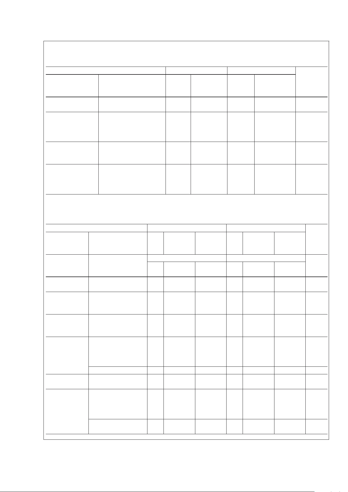
Electrical Characteristics (Continued)
VIN=VO+ 5V, IO= 1A, CO= 22 µF, unless otherwise specified. Boldface limits apply over the entire operating temperature range of the indicated device. All other specifications apply for T
A=TJ
= 25˚C.
Output Voltage (V
O
) 9V 10V
Units
Parameter Conditions Typ
LM2940
Typ
LM2940
Limit Limit
(Note 4) (Note 4)
Short Circuit (Note 6) 1.9 1.6 1.9 1.6 A
MIN
Current
Maximum Line R
O
= 100Ω
Transient T ≤ 100 ms
LM2940 75 60/60 75 60/60 V
MIN
LM2940C 55 45
Reverse Polarity R
O
= 100Ω
DC Input Voltage LM2940 −30 −15/−15 −30 −15/−15 V
MIN
LM2940C −30 −15
Reverse Polarity R
O
= 100Ω
Transient Input T ≤ 100 ms
Voltage LM2940 −75 −50/−50 −75 −50/−50 V
MIN
LM2940C −55 −45/−45
Electrical Characteristics
VIN=VO+ 5V, IO= 1A, CO= 22 µF, unless otherwise specified. Boldface limits apply over the entire operating temperature range of the indicated device. All other specifications apply for T
A=TJ
= 25˚C.
Output Voltage (V
O
) 12V 15V
Units
LM2940 LM2940/833 LM2940 LM2940/833
Parameter Conditions Typ Limit Limit Typ Limit Limit
(Note 4) (Note 5) (Note 4) (Note 5)
13.6V ≤ V
IN
≤ 26V 16.75V ≤ VIN≤ 26V
Output Voltage 5 mA ≤ I
O
≤1A 12.00 11.64/11.40 11.64/11.40 15.00 14.55/14.25 14.55/14.25 V
MIN
12.36/12.60 12.36/12.60 15.45/15.75 15.45/15.75 V
MAX
Line Regulation VO+2V≤ VIN≤ 26V, 20 120 75/120 20 150 95/150 mV
MAX
IO=5mA
Load Regulation 50 mA ≤ I
O
≤ 1A
LM2940, LM2940/883 55 120/200 120/190 150/240 mV
MAX
LM2940C 55 120 70 150
Output 100 mADC and
Impedance 20 mArms, 80 1000/1000 100 1000/1000 mΩ
f
O
= 120 Hz
Quiescent
Current
V
O
+2V ≤ VIN≤ 26V,
I
O
=5mA
LM2940, LM2940/883 10 15/20 15/20 15/20 mA
MAX
LM2940C 10 15 10 15
V
IN=VO
+ 5V, IO= 1A 30 45/60 50/60 30 45/60 50/60 mA
MAX
Output Noise 10 Hz − 100 kHz, 360 1000/1000 450 1000/1000 µV
rms
Voltage IO=5mA
Ripple Rejection f
O
= 120 Hz, 1 V
rms
,
I
O
= 100 mA
LM2940 66 54/48 dB
MIN
LM2940C 66 54 64 52
f
O
= 1 kHz, 1 V
rms
,
52/46 48/42
dB
MIN
IO=5mA
LM2940/LM2940C
www.national.com 6
 Loading...