

NSC LM2889N Datasheet
LM2889 TV Video Modulator
General Description
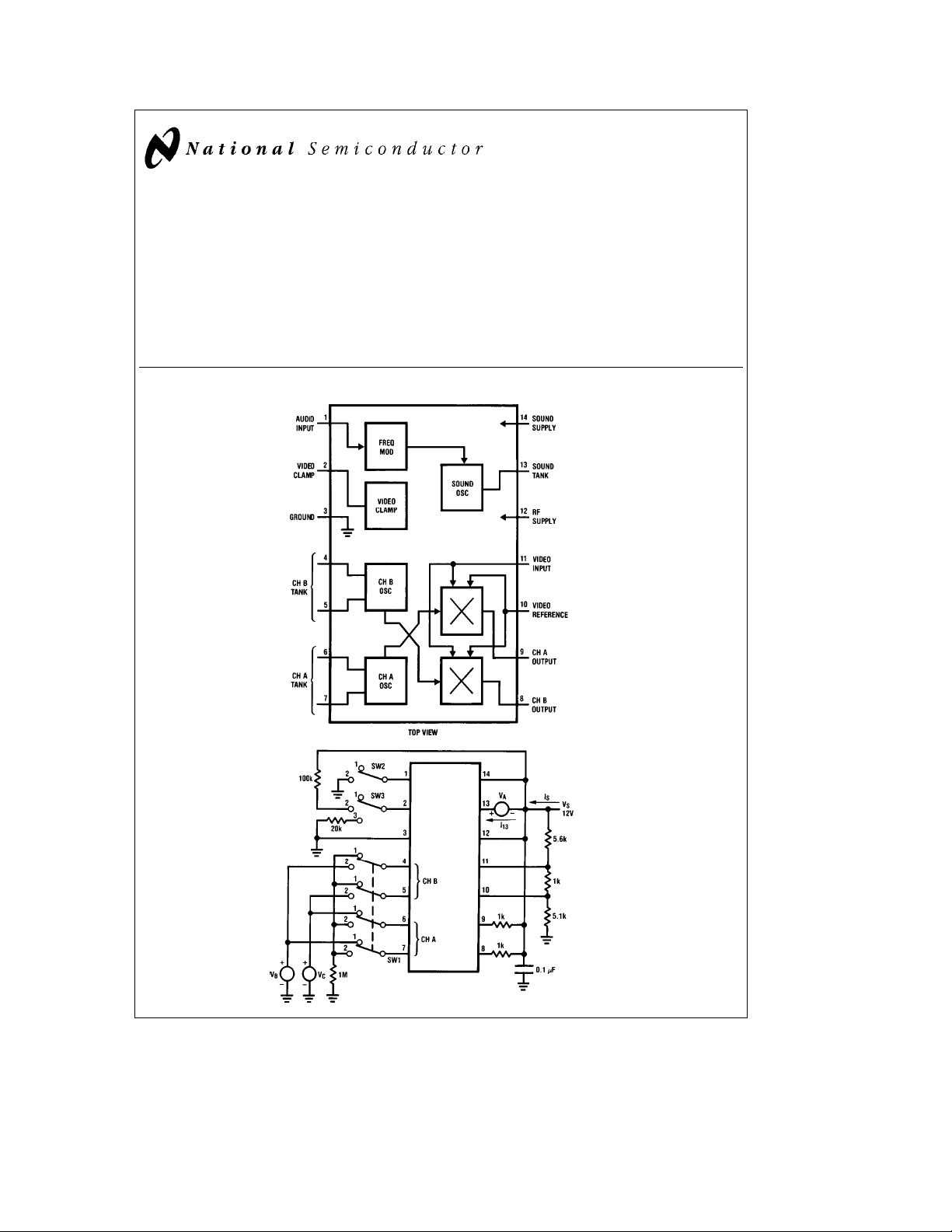
The LM2889 is designed to interface audio and video signals to the antenna terminals of a TV receiver. It consists of
a sound subcarrier oscillator and FM modulator, video
clamp, and RF oscillators and modulators for two low-VHF
channels.
The LM2889 allows video information from VTRs, video disk
systems, games, test equipment, or similar sources to be
displayed on black and white or color TV receivers.
Block and Connection Diagrams (Dual-In-Line Package)
Features
Y
Pin for pin compatible with LM1889 RF section
Y
Low distortion FM sound modulator (less than 1%
THD)
Y
Video clamp for AC-coupled video
Y
Low sound oscillator harmonic levels
Y
10V to 16V supply operation
Y
DC channel switching
Y
Excellent oscillator stability
Y
Low intermodulation products
LM2889 TV Video Modulator
December 1994
Order Number LM2889N
See NS Package Number N14A
DC Test Circuit
TL/H/5079– 1
C
1995 National Semiconductor Corporation RRD-B30M115/Printed in U. S. A.
TL/H/5079
Absolute Maximum Ratings
If Military/Aerospace specified devices are required,
please contact the National Semiconductor Sales
Office/Distributors for availability and specifications.
Supply Voltage 18V
Power Dissipation Package (Note 1) 700 mW
Operating Temperature Range 0
§
DC
Ctoa70§C
Storage Temperature Range
(V14–V13) Max
(V12–V8) Max 7V
(V12–V9) Max 7V
b
55§Ctoa150§C
g
5V
DC
DC
DC
Lead Temperature (Soldering, 10 seconds) 260§C
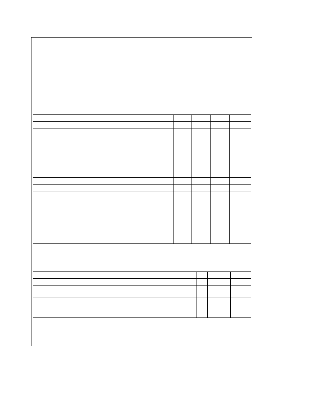
DC Electrical Characteristics
(DC test circuit, all switches normally pos. 1, V
e
S
Parameter Conditions Min Typ Max Units
Supply Current I
Sound Oscillator Current DI
Sound Oscillator Zener Current I
Sound Modulator Audio Current DI
S
13
13
Change VAfromb2V toa2V 0.2 0.35 0.6 mA
Change SW2 from Pos. 1 to Pos. 2 0.9 mA
13
Video Clamp Voltage V2
Unloaded 5.0 5.25 5.5 V
Loaded SW3 Pos. 3 5.1 V
Video Clamp Capacitor Discharge SW3 Pos. 2
Current (V
S
–V2)/10
5
Ch. A Oscillator OFF Voltage, V6, V7 SW1 Pos. 2 2 mV
Ch. A Oscillator Current Level I
7
e
V
B
Ch. B Oscillator OFF Voltage V4, V5 2 mV
Ch. B Oscillator Current Level I
4
SW1 Pos. 2, V
Ch. A Modulator Conversion Ratio Measure DV9 by Changing from
DV9/(V11-V10) V
e
B
e
V
C
Ch. B Modulator Conversion Ratio SW1 Pos. 2, Measure DV8 by
DV8/(V11–V10) Changing from V
to V
B
V11–V10
e
12V, V
A
e
10V, V
C
e
10V, V
C
10V; Divide by V11–V10
e
11V, V
e
2V, V
V
B
11V 2.5 3.5 5.0 mA
e
B
11V, to V
e
C
e
10V, V
C
e
B
e
10V, V
B
10V; Divide by
e
10V)
C
10 16 25 mA
0.85 mA
20 mA
11V 2.5 3.5 5.0 mA
11V, 0.3 0.50 0.75 V/V
e
11V,
C
0.3 0.50 0.75 V/V
DC
DC
DC
DC
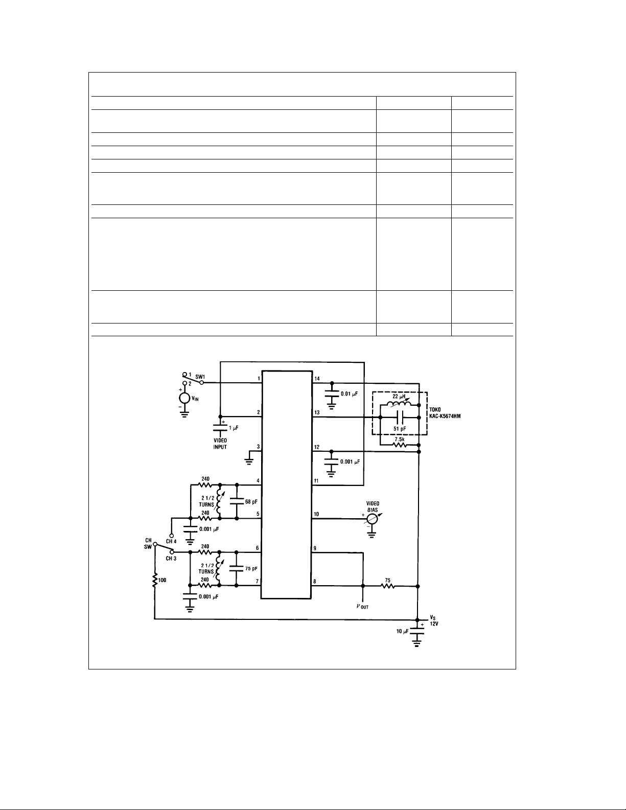
AC Electrical Characteristics (AC test circuit, V
e
12V)
S
Parameter Conditions Min Typ Max Units
Sound Carrier Oscillator Level (V13) 3.4 Vp-p
Sound Modulator Deviation Df/DVIN, SW1 Pos. 2, Change VINfrom 1.4V
to 1.0V, Measure Df at Pin 13, Divide as Shown
250 Hz/mV
Ch. 3 RF Oscillator Level n6, n7 Ch. Sw. Pos. 3, fe61.25 MHz, Use FET Probe 550 mVp-p
Ch. 4 RF Oscillator Level, n4, n5, Ch. Sw. Pos. 4, fe67.25 MHz, Use FET Probe 550 mVp-p
RF Modulator Conversion Gain n
Note 1: For operation in ambient temperatures above 25§C, the device must be derated based on a 150§C maximum junction temperature and a thermal resistance
C/W junction to ambient.
of 80
§
Note 2: Conversion gain shown is measured with 75 X input RF meter which makes the AC RF output load 37.5X.
/(V10±V11) Ch. Sw. Pos. 3, fe61.25 MHz. (Note 2) 10 mVrms/V
OUT
2
Design Characteristics (AC test circuit, V
Parameter Typ Units
Sound Modulator Audio THD atg25 kHz Deviation, VINmust be 1 kHz Source, 0.8 %
Demodulate as Shown in
Sound Modulator Input Impedance (Pin 1) 1.5 kX
Sound Modulator Bandwidth 100 kHz
Oscillator Supply Dependence, Sound Carrier, RF See Curves
Oscillator Temperature Dependence (IC Only)
Sound Carrier
RF
RF Oscillator Maximum Operating Frequency (Temperature Stability Degraded) 100 MHz
RF Modulator
Carrier Suppression (Adjust Video Bias for Minimum RF Carrier at n
and Reference to n
Information, RF Modulation Section)
3.58 MHz Differential Gain 5 %
Differential Phase 3 degrees
2.5V Vp-p Video, 87.5% Mod
Output Harmonics below RF Carrier
2nd, 3rd
4th and Above
Input Impedance, Pin 10, Pin 11 1 MX//2 pF
Figure 1
with 3V Offset at Pins 10 and 11, See Applications
OUT
e
12V)
S
b
15 ppm/§C
b
50 ppm/§C
OUT
30 dB
b
12 dB
b
20 dB
AC Test Circuit
TL/H/5079– 2
3
 Loading...