

LM2879 Dual 8W Audio Amplifier
LM2879 Dual 8W Audio Amplifier
February 1995
General Description
Y
The LM2879 is a monolithic dual power amplifier which offers high quality performance for stereo phonographs, tape
players, recorders, AM-FM stereo receivers, etc.
The LM2879 will deliver 8W/channel to an 8X load. The
Self-centering biasing
Y
4MXinput impedance
Y
Internal current limiting
Y
Internal thermal protection
amplifier is designed to operate with a minimum of external
components and contains an internal bias regulator to bias
each amplifier. Device overload protection consists of both
internal current limit and thermal shutdown.
Features
Y
AVOtypical 90 dB
Y
9W per channel (typical)
Y
60 dB ripple rejection
Y
70 dB channel separation
Applications
Y
Multi-channel audio systems
Y
Tape recorders and players
Y
Movie projectors
Y
Automotive systems
Y
Stereo phonographs
Y
Bridge output stages
Y
AM-FM radio receivers
Y
Intercoms
Y
Servo amplifiers
Y
Instrument systems
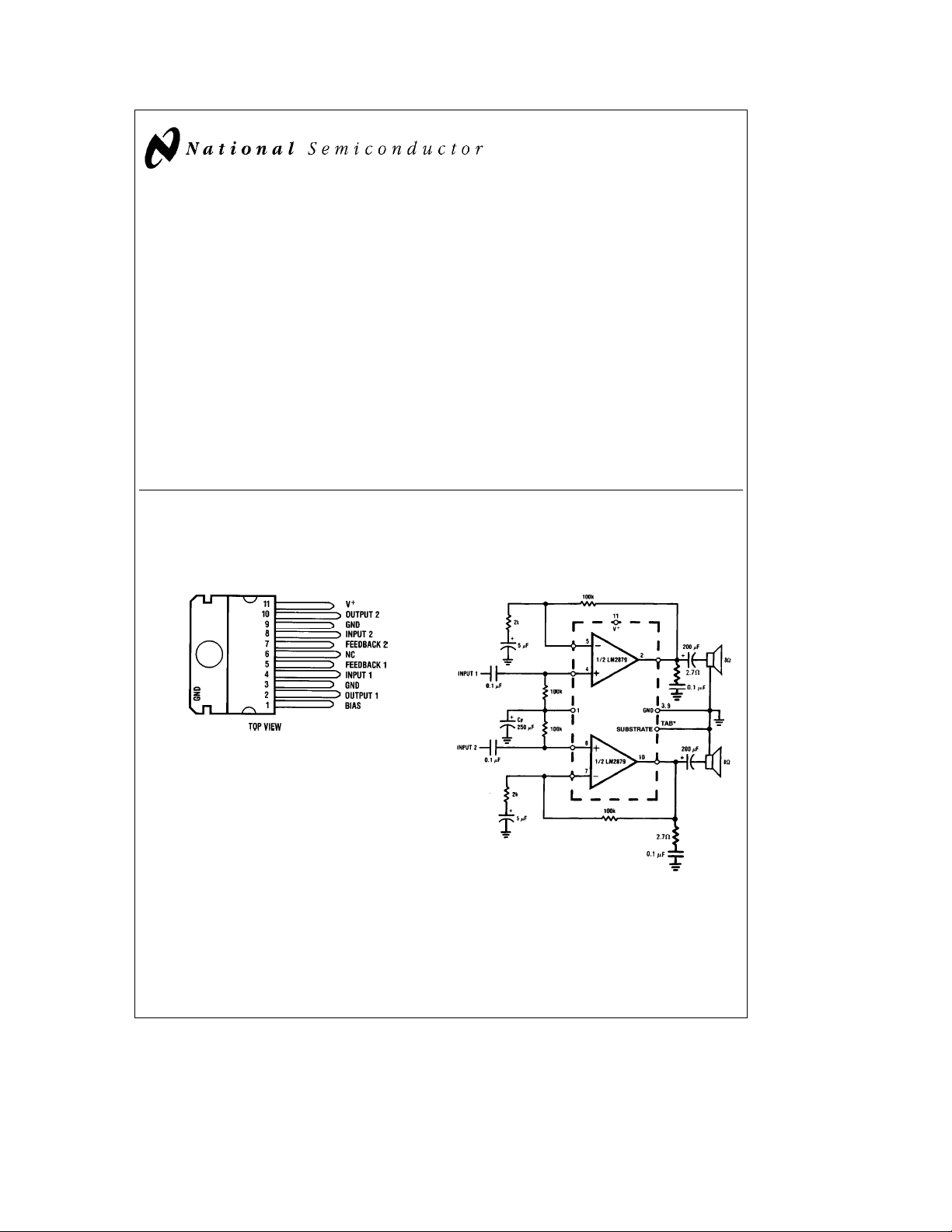
Connection Diagram and Typical Application
Plastic Package
Stereo Amplifier
TL/H/5291– 1
Order Number LM2879T
See NS Package Number TA11B
*TAB must be connected to GND.
TL/H/5291– 2
FIGURE 1
C
1995 National Semiconductor Corporation RRD-B30M115/Printed in U. S. A.
TL/H/5291
Absolute Maximum Ratings
If Military/Aerospace specified devices are required,
please contact the National Semiconductor Sales
Office/Distributors for availability and specifications.
Supply Voltage 35V
Input Voltage (Note 1)
Operating Temperature (Note 2) 0
Electrical Characteristics V
Ctoa70§C
§
e
28V, T
S
g
0.7V
TAB
Storage Temperature
Junction Temperature 150
Lead Temp. (Soldering, 10 seconds) 260
ESD rating to be determined.
Thermal Resistance
i
JC
i
JA
e
25§C, R
e
L
8X,A
e
50 (34 dB), unless otherwise specified.
V
Parameter Conditions Min Typ Max Units
Total Supply Current P
e
0W 12 65 mA
O
Operating Supply Voltage 6 32 V
Output Power/Channel fe1 kHz, THDe10%, T
Distortion fe1 kHz, R
Output Swing R
Channel Separation C
PSRR Positive Supply C
P
O
L
BYPASS
e
f
V
O
BYPASS
e
f
V
ripple
e
8X
L
e
1 W/Channel
e
8X V
e
50 mF, C
1 kHz, Output Referred
e
4 Vrms
e
50 mF, C
120 Hz, Output Referred
e
1 Vrms
PSRR Negative Supply Measured at DC, Input Referred
Common-Mode Range Split Suppliesg15V, Pin 1
Tied to Pin 11
e
25§C6 8 W
TAB
0.05 1 %
b
6V Vp-p
e
0.1 mF
IN
e
0.1 mF
IN
b
50
b
50
S
b
70 dB
b
60 dB
b
60 dB
g
13.5 V
Input Offset Voltage 10 mV
Noise Equivalent Input Noise
Open Loop Gain R
e
e
0, C
R
S
BW
CCIR
Output Noise Wideband 0.8 mV
e
R
S
e
S
0.1 mF
IN
e20b
20 kHz 2.5 mV
ARM 3.0 mV
#
e
0, C
0.1 mF, A
IN
51X,fe1 kHz, R
e
200
V
e
8X 70 dB
L
Input Bias Current 100 nA
Input Impedance Open Loop 4 MX
DC Output Voltage V
e
28V 14 V
S
Slew Rate 2V/ms
Power Bandwidth 3 dB Bandwidth at 2.5W 65 kHz
Current Limit 1.5 A
Note 1: The input voltage range is normally limited tog0.7V with respect to pin 1. This range may be extended by shorting pin 1 to the positive supply.
Note 2: For operation at ambient temperature greater than 25
resistance, junction to case, is 3
C/W. Thermal resistance, case to ambient, is 40§C/W.
§
C, the LM2879 must be derated based on a maximum 150§C junction temperature. Thermal
§
b
65§Ctoa150§C
43§C/W
1§C/W
C
§
C
§
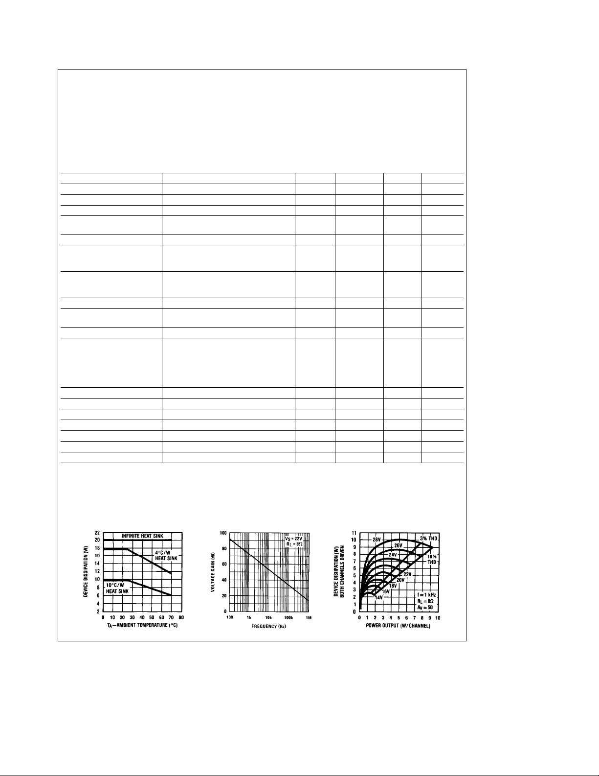
Typical Performance Characteristics
Device Dissipation vs
Ambient Temperature
Open Loop Gain vs
Frequency
Power Dissipation vs
Power Output
TL/H/5291– 3
2
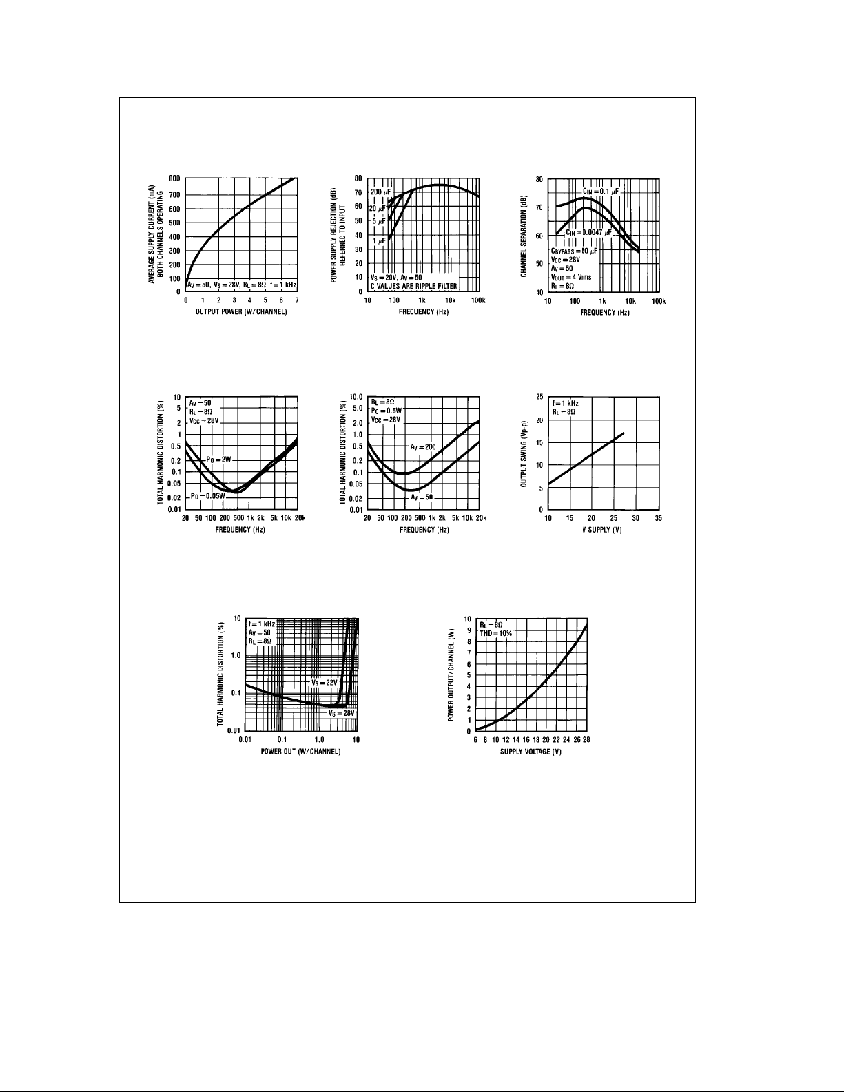
Typical Performance Characteristics (Continued)
Supply Current vs Output
Power
Supply Rejection vs
Frequency
Channel Separation
(Referred to the Output)
Frequency
Total Harmonic Distortion
vs Frequency
Total Harmonic Distortion
vs Power Output
Total Harmonic Distortion
vs Frequency Output Swing vs V
Power Output/Channel vs
Supply Voltage
S
TL/H/5291– 4
3
 Loading...