

NSC LM2878P Datasheet
LM2878 Dual 5 Watt Power Audio Amplifier
LM2878 Dual 5 Watt Power Audio Amplifier
December 1994
General Description
The LM2878 is a high voltage stereo power amplifier designed to deliver 5W/channel continuous into 8X loads. The
amplifier is ideal for use with low regulation power supplies
due to the absolute maximum rating of 35V and its superior
power supply rejection. The LM2878 is designed to operate
with a low number of external components, and still provide
flexibility for use in stereo phonographs, tape recorders, and
AM-FM stereo receivers. The flexibility of the LM2878 allows it to be used as a power operational amplifier, power
comparator or servo amplifier. The LM2878 is internally
compensated for all gains greater than 10, and comes in an
11-lead single-in-line package (SIP). The package has been
redesigned, resulting in the slightly degraded thermal characteristics shown in the figure Device Dissipation vs Ambient Temperature.
Typical Applications
Features
Y
Wide operating range 6V –32V
Y
5W/channel output
Y
60 dB ripple rejection, output referred
Y
70 dB channel separation, output referred
Y
Low crossover distortion
Y
AC short circuit protected
Y
Internal thermal shutdown
Applications
Y
Stereo phonographs
Y
AM-FM radio receivers
Y
Power op amp, power comparator
Y
Servo amplifiers
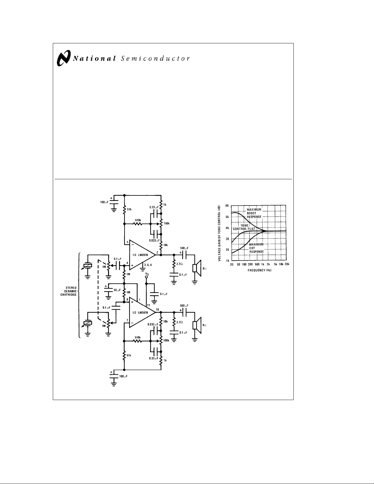
Frequency Response
of Bass Tone Control
TL/H/7934– 2
TL/H/7934– 1
FIGURE 1. Stereo Phonograph Amplifier with Bass Tone Control
C
1995 National Semiconductor Corporation RRD-B30M115/Printed in U. S. A.
TL/H/7934
Absolute Maximum Ratings
If Military/Aerospace specified devices are required,
please contact the National Semiconductor Sales
Office/Distributors for availability and specifications.
Supply Voltage 35V
Input Voltage (Note 1)
Operating Temperature (Note 2) 0§Ctoa70§C
Electrical Characteristics V
g
0.7V
e
22V, T
S
TAB
Storage Temperature
Junction Temperature
Lead Temperature (Soldering, 10 sec.)
Thermal Resistance
i
JC
i
JA
e
25§C, R
e
L
8X,A
e
50 (34 dB) unless otherwise specified.
V
b
65§Ctoa150§C
a
a
10§C/W
55§C/W
150§C
260§C
Parameter Conditions Min Typ Max Units
Total Supply Current P
e
0W 10 50 mA
O
Operating Supply Voltage 6 32 V
Output Power/Channel fe1 kHz, THDe10%, T
e
f
1 kHz, THDe10%, V
Distortion fe1 kHz, R
e
P
O
e
P
O
e
P
O
Output Swing R
Channel Separation C
PSRR Power Supply C
Rejection Ratio f
e
L
BYPASS
e
f
1 kHz, Output Referred
e
V
O
BYPASS
e
120 Hz, Output Referred
V
ripple
e
8X
L
50 mW
0.5W 0.15 %
2W 0.14 %
8X V
e
50 mF, C
4 Vrms
e
50 mF, C
e
1 Vrms
PSRR Negative Supply Measured at DC, Input Referred
Common-Mode Range Split Suppliesg15V, Pin 1
Tied to Pin 11
e
25§C 5 5.5 W
TAB
e
12V 1.3 W
S
0.20 %
b
6V Vp-p
S
e
0.1 mF
IN
e
0.1 mF
IN
b
50
b
50
b
70 dB
b
60 dB
b
60 dB
g
13.5 V
Input Offset Voltage 10 mV
Noise Equivalent Input Noise
e
0, C
e20b
e
0.1 mF 2.5 mV
IN
20 kHz
R
BW
S
CCIR#ARM 3.0 mV
Open Loop Gain R
Output Noise Wideband
e
R
S
S
e
0, C
0.1 mF, A
IN
e
51X,fe1 kHz, R
e
200
V
e
8X 70 dB
L
0.8 mV
Input Bias Current 100 nA
Input Impedance Open Loop 4 MX
DC Output Voltage V
e
22V 10 11 12 V
S
Slew Rate 2V/mS
Power Bandwidth 3 dB Bandwidth at 2.5W 65 kHz
Current Limit 1.5 A
Note 1:g0.7V applies to audio applications; for extended range, see Application Hints.
Note 2: For operation at ambient temperature greater than 25
resistance which depends upon device mounting techniques.
C, the LM2878 must be derated based on a maximum 150§C junction temperature using a thermal
§
2
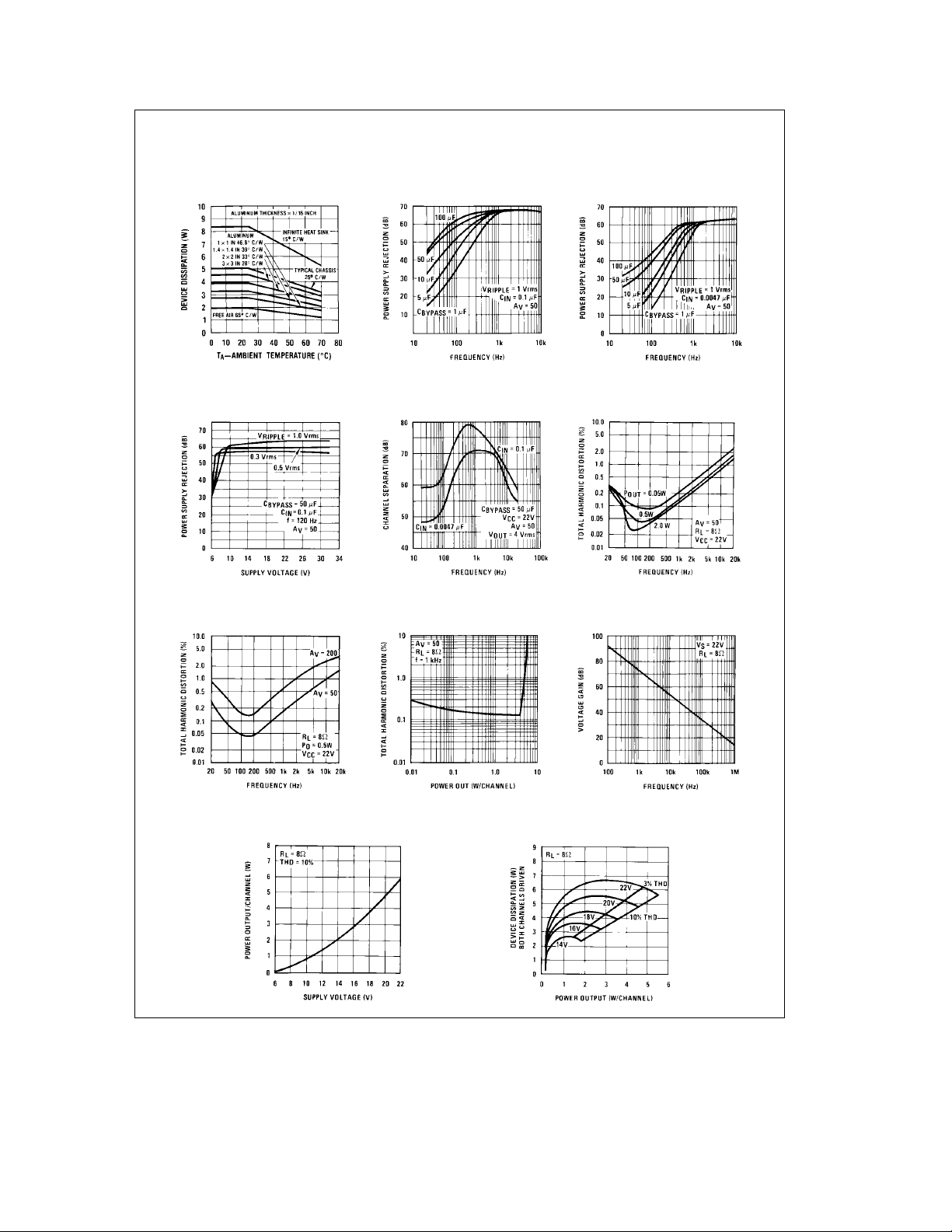
Typical Performance Characteristics
Device Dissipation vs
Ambient Temperature
Power Supply Rejection
Ratio (Referred to the
Output) vs Supply Voltage
Total Harmonic Distortion
vs Frequency
Power Supply Rejection
Ratio (Referred to the
Output) vs Frequency
Channel Separation
(Referred to the Output) vs
Frequency
Total Harmonic Distortion
vs Power Out
Power Supply Rejection
Ratio (Referred to the
Output) vs Frequency
Total Harmonic Distortion
vs Frequency
Open Loop Gain vs
Frequency
Power Output/Channel vs
Supply Voltage
Power Dissipation vs
Power Out
TL/H/7934– 3
3
 Loading...