

NSC LM2853MHX-3.3, LM2853 Datasheet
LM2853
3A 550 kHz Synchronous SIMPLE SWITCHER
Regulator
®
Buck
LM2853 3A 550 kHz Synchronous SIMPLE SWITCHER
October 2006
General Description
The LM2853 synchronous SIMPLE SWITCHER®buck regulator is a 550 kHz step-down switching voltage regulator
capable of driving up to a 3A load with excellent line and load
regulation. The LM2853 accepts an input voltage between
3.0V and 5.5V and delivers a customizable output voltage
that is factory programmable from 0.8V to 3.3V in 100mV
increments. Internal type-three compensation enables a low
component count solution and greatly simplifies external
component selection. The exposed-pad TSSOP-14 package
enhances the thermal performance of the LM2853.
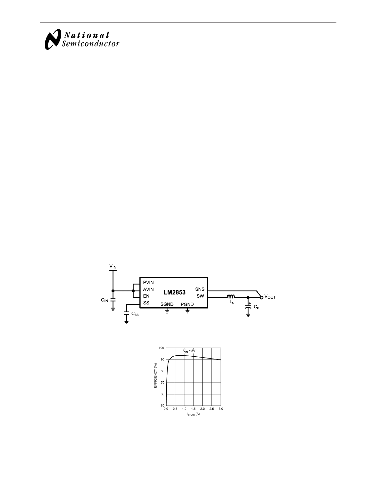
Typical Application Circuit
Features
n Input voltage range of 3.0V to 5.5V
n Factory EEPROM set output voltages from 0.8V to 3.3V
in 100 mV increments
n Maximum load current of 3A
n Voltage Mode Control
n Internal type-three compensation
n Switching frequency of 550 kHz
n Low standby current of 12 µA
n Internal 40 mΩ MOSFET switches
n Standard voltage options
0.8/1.0/1.2/1.5/1.8/2.5/3.0/3.3 volts
n Exposed pad TSSOP-14 package
Applications
n Low voltage point of load regulation
n Local solution for FPGA/DSP/ASIC core power
n Broadband networking and communications
infrastructure
®
Buck Regulator
20201502
Efficiency vs Load Current (V
SIMPLE SWITCHER®is a Registered Trademark of National Semiconductor Corporation.
© 2006 National Semiconductor Corporation DS202015 www.national.com
OUT
20201501
= 3.3V)
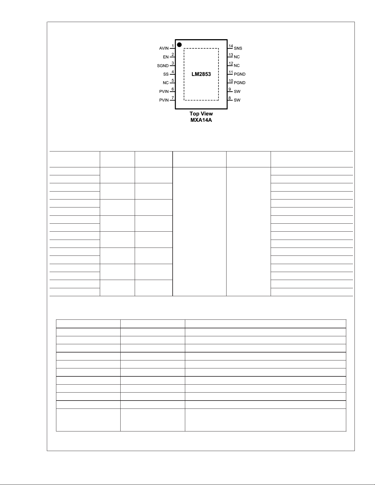
Connection Diagram
LM2853
Ordering Information
20201503
Voltage
Order Number
LM2853MH-0.8
LM2853MHX-0.8 2500 Units, Tape and Reel
LM2853MH-1.0
LM2853MHX-1.0 2500 Units, Tape and Reel
LM2853MH-1.2
LM2853MHX-1.2 2500 Units, Tape and Reel
LM2853MH-1.5
LM2853MHX-1.5 2500 Units, Tape and Reel
LM2853MH-1.8
LM2853MHX-1.8 2500 Units, Tape and Reel
LM2853MH-2.5
LM2853MHX-2.5 2500 Units, Tape and Reel
LM2853MH-3.0
LM2853MHX-3.0 2500 Units, Tape and Reel
LM2853MH-3.3
LM2853MHX-3.3 2500 Units, Tape and Reel
Note: Contact factory for other voltage options.
Option
0.8 LM2853-0.8
1.0 LM2853-1.0
1.2 LM2853-1.2
1.5 LM2853-1.5
1.8 LM2853-1.8
2.5 LM2853-2.5
3.0 LM2853-3.0
3.3 LM2853-3.3
Package
Marking Package Type
TSSOP-14 exposed
pad
Package
Drawing Supplied As
94 Units, Rail
94 Units, Rail
94 Units, Rail
94 Units, Rail
MXA14A
94 Units, Rail
94 Units, Rail
94 Units, Rail
94 Units, Rail
Pin Descriptions
Pin # Name Function
1 AVIN Input Voltage for Control Circuitry.
2 EN Enable.
3 SGND Low noise ground.
4 SS Soft-Start Pin.
5 NC No Connect. This pin must be tied to ground.
6,7 PVIN Input Voltage for Power Circuitry.
8,9 SW Switch Pin.
10,11 PGND Power Ground.
12,13 NC No-Connect. These pins must be tied to ground.
14 SNS Output Voltage Sense Pin.
Exposed Pad EP The exposed pad is internally connected to GND, but it cannot be
used as the primary GND connection. The exposed pad should be
soldered to an external GND plane.
www.national.com 2
LM2853
Absolute Maximum Ratings (Note 1)
If Military/Aerospace specified devices are required,
please contact the National Semiconductor Sales Office/
Distributors for availability and specifications.
14-Pin Exposed Pad TSSOP Package
Infrared (15 sec) 220˚C
Vapor Phase (60 sec) 215˚C
Soldering (10 sec) 260˚C
AVIN, PVIN, EN, SNS, SW, SS −0.3V to 6.0V
ESD Susceptibility (Note 2) 2kV
Operating Ratings (Note 1)
Power Dissipation Internally Limited
Storage Temperature Range −65˚C to +150˚C
Maximum Junction Temp. 150˚C
PVIN to GND 1.5V to 5.5V
AVIN to GND 3.0V to 5.5V
Junction Temperature −40˚C to +125˚C
Electrical Characteristics Specifications with standard typeface are for T
= 25˚C, and those in bold face
J
type apply over the full Junction Temperature Range (−40˚C to 125˚C). Minimum and Maximum limits are guaranteed through
test, design or statistical correlation. Typical values represent the most likely parametric norm at T
= 25˚C and are provided
J
for reference purposes only. Unless otherwise specified AVIN = PVIN = 5V.
Symbol Parameter Conditions Min Typ Max Units
SYSTEM PARAMETERS
V
OUT
∆V
/∆AVIN Line Regulation (Note 3) V
OUT
Voltage Tolerance (Note 3) V
= 0.8V option 0.782 0.8 0.818
OUT
V
= 1.0V option 0.9775 1.0 1.0225
OUT
V
= 1.2V option 1.1730 1.2 1.227
OUT
V
= 1.5V option 1.4663 1.5 1.5337
OUT
V
= 1.8V option 1.7595 1.8 1.8405
OUT
V
= 2.5V option 2.4437 2.5 2.5563
OUT
V
= 3.0V option 2.9325 3.0 3.0675
OUT
V
= 3.3V option 3.2257 3.3 3.3743
OUT
= 0.8V, 1.0V, 1.2V, 1.5V,
OUT
0.2 1.1 %
1.8V or 2.5V
3.0V ≤ AVIN ≤ 5.5V
= 3.0V or 3.3V
V
OUT
0.2 1.1 %
3.5V ≤ AVIN ≤ 5.5V
∆V
V
ON
OUT
/∆I
Load Regulation Normal operation 2 mV/A
O
UVLO Threshold (AVIN) Rising 2.47 3.0 V
Falling Hysteresis 50 155 260 mV
R
DS(ON)-P
R
DS(ON)-N
R
SS
I
CL
I
Q
I
SD
R
SNS
PFET On Resistance Isw = 3A 40 120 mΩ
NFET On Resistance Isw = 3A 32 100 mΩ
Soft-Start Resistance 450 kΩ
Peak Current Limit Threshold 3.6 5A
Operating Current Non-switching 0.85 2 mA
Shutdown Quiescent Current EN = 0V 12 50 µA
Sense Pin Resistance 432 kΩ
PWM
f
D
osc
range
Switching Frequency . 325 550 725 kHz
Duty Cycle Range 0 100 %
ENABLE CONTROL (Note 4)
V
IH
V
IL
I
EN
EN Pin Minimum High Input 75 %of
EN Pin Maximum Low Input 25 %of
EN Pin Pullup Current EN = 0V 1.5 µA
V
AVIN
AVIN
www.national.com3
Electrical Characteristics Specifications with standard typeface are for T
apply over the full Junction Temperature Range (−40˚C to 125˚C). Minimum and Maximum limits are guaranteed through test,
LM2853
design or statistical correlation. Typical values represent the most likely parametric norm at T
= 25˚C, and those in bold face type
J
= 25˚C and are provided for
J
reference purposes only. Unless otherwise specified AVIN = PVIN = 5V. (Continued)
Symbol Parameter Conditions Min Typ Max Units
THERMAL CONTROLS
T
SD
T
SD-HYS
Thermal Shutdown Threshold 165 ˚C
Hysteresis for Thermal
10 ˚C
Shutdown
THERMAL RESISTANCE
θ
JA
Note 1: Absolute maximum ratings indicate limits beyond which damage to the device may occur. Operating Range indicates conditions for which the device is
intended to be functional, but does not guarantee specific performance limits. For guaranteed specifications and test conditions, see the Electrical Characteristics.
Note 2: The human body model is a 100 pF capacitor discharged through a 1.5 kΩ resistor into each pin. Test Method is per JESD22-AI14.
Note 3: V
Note 4: The enable pin is internally pulled up, so the LM2853 is automatically enabled unless an external enable voltage is applied.
Junction to Ambient MXA14A 38 ˚C/W
measured in a non-switching, closed-loop configuration at the SNS pin.
OUT
www.national.com 4
 Loading...